Si114x-中文手册
114智能制造质量智能监控系统_用户手册

智能制造质量智能监控系统V1.0使用说明书一、引言文章摘要本文档详细描述关于如何利用各模块的设置对系统进行日常管理、维护、统计。
读者对象本文档的读者对象为系统的使用者,或者指导最终用户使用本系统的相关人员。
我们假定最终用户已掌握如下知识:⊙Windows/win7/win8/win10等操作系统的使用;⊙Chome浏览器/搜狗浏览器/360浏览器/IE等浏览器的使用;⊙基本的Internet的原理常识。
1.1登录启动并运行系统,可以在电脑的桌面,找到系统软件的图标,双击鼠标的左键就可以启动并运行了;另外一种,你也可以在电脑的“开始菜单”中找到系统软件的快速启动方式,点击鼠标左键一样可以打开运行。
成功启动并运行系统后,马上就会进入到系统的登录界面,如下图:用户输入用户名和密码时需要注意以下几点:用户名和密码登录密码需在8-16位之间,由数字和字母组成。
用户名和密码不能输入空格键。
管理员的默认用户名是admin密码是12345678。
成功启动并运行系统后,马上就会进入到系统的登录界面,操作人员必须输入正确的:用户名、密码才能进入系统,如果操作员输入的信息不合法,系统将会立即提示你“用户名或密码错误”,必须在登录成功之后才能进入软件的主界面,输入错误就会提示失败输入的用户名或密码错误,这时候要求重新输入,只有输入正确之后才能进入主界面。
1.2首页当用户通过管理员账号或者重新注册的账号登录系统,进入到系统的第一个界面时,用户可以查看系统的主页信息,登陆系统以后系统会自动下载补丁进行系统升级。
但是当前系统为最新系统,所以不需要更新升级,然后用户可以看到系统的主要菜单,系统的主要模块菜单都有功能菜单即系统的子菜单,详情如下图所示:用户能够清楚的在界面内看到系统的主要功能和系统的状态指示。
根据实际的需求,用户可以在界面内进行相应的功能操作。
非常的简单方便。
1.3通讯连接在首页界面的导航栏中有一个通讯连接选项,点击通讯连接选项,进入到通讯连接控制界面中,该界面中显示了一些通讯连接的信息,节省了用户的管理时间,提高了工作效率,详情如下图所示:1.4制造控制中心在当前系统的菜单界面上,找到控制中心按钮,点击鼠标左键打开子页面之后,就可以操作子页面的相关信息;在子页面中,按照一般我们的操作习惯,点击子页面的操作按钮/选项,就能进入到子页面上所包含的有相应的模块功能;页面上对每个独立的模块都有比较详细的操作功能流程说明,可以根据流程说明进行具体的操作,详情如下图所示:1.5监控管理用户在使用本系统进行监控管理的过程中,为了方便用户进行管理,可以在系统内,进行监控管理的新增功能,方便用户进行监控管理,也节省了用户的核算时间,提高了核算效率,点击界面内的监控管理按键,系统弹出对应的窗口。
LPC1114的IO配置部分的中文手册

表111. LPC111x 引脚配置引脚配置--图8–10引脚描述表8–114引脚配置--图8–10引脚描述表8–114引脚配置图8–8-图8–10引脚描述表8–112表8–114图8–10表8–112表8–113表8–1143. LPC111x 引脚描述表 112. LPC1113/14 引脚描述表 (LQFP48 封装)RESET — 外部复位输入:此引脚上的低电平会使设备复位,I/O 端口和外设复位成初始的默认状态,并使处理器从0地址开始执行。
I/O PIO0_0 — 通用数字输入/输出引脚。
PIO0_1/CLKOUT/ CT32B0_MAT2PIO0_2/SSEL0/ CT16B0_CAP04[1]I/O PIO0_1 —通用数字输入/输出引脚。
复位时低电平启动在线系统编程命令处 理程序。
O CLKOUT — 时钟输出脚。
OCT32B0_MAT2 —32位定时器0匹配输出2。
10[1]I/O PIO0_2 —通用数字输入/输出引脚。
O SSEL0 —SPI0从机选择。
ICT16B0_CAP0 —16位定时器0捕获输入0。
PIO0_314[1] I/OPIO0_3 —通用数字输入/输出引脚。
.I/O SCK0 —SPI0串行时钟。
PIO0_7/CTS 23[1] I/O PIO0_7 —通用数字输入/输出引脚(大电流输出驱动器)。
I CTS —UART清除发送。
PIO0_8/MISO0/CT16B0_MAT0PIO0_9/MOSI0/CT16B0_MAT1 SWCLK/PIO0_10/ SCK0/CT16B0_MAT2TDI/PIO0_11/AD0/CT32B0_MAT3 TMS/PIO1_0/AD1/CT32B1_CAP0 TDO/PIO1_1/AD2/CT32B1_MAT0TRST/PIO1_2/AD3/CT32B1_MAT1 27[1] I/O PIO0_8 —通用数字输入/输出引脚。
13x_14x_14x1数据手册
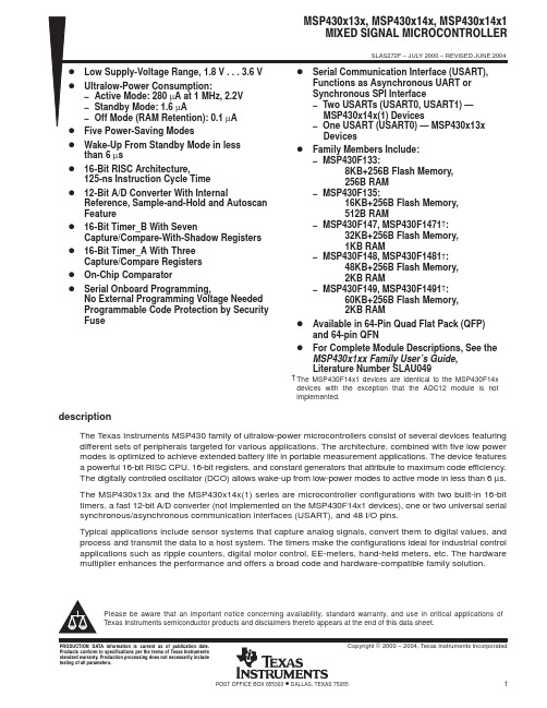
10 11 12 13 14 15
33 16 17 18 19 20 21 22 23 24 25 26 27 28 29 30 31 32
2
P1.5/TA0 P1.6/TA1 P1.7/TA2 P2.0/ACLK P2.1/TAINCLK P2.2/CAOUT/TA0 P2.3/CA0/TA1 P2.4/CA1/TA2 P2.5/Rosc P2.6/ADC12CLK P2.7/TA0 P3.0/STE0 P3.1/SIMO0 P3.2/SOMI0 P3.3/UCLK0 P3.4/UTXD0
D
D D
† The MSP430F14x1 devices are identical to the MSP430F14x devices with the exception that the ADC12 module is not implemented.
description
The Texas Instruments MSP430 family of ultralow-power microcontrollers consist of several devices featuring different sets of peripherals targeted for various applications. The architecture, combined with five low power modes is optimized to achieve extended battery life in portable measurement applications. The device features a powerful 16-bit RISC CPU, 16-bit registers, and constant generators that attribute to maximum code efficiency. The digitally controlled oscillator (DCO) allows wake-up from low-power modes to active mode in less than 6 µs. The MSP430x13x and the MSP430x14x(1) series are microcontroller configurations with two built-in 16-bit timers, a fast 12-bit A/D converter (not implemented on the MSP430F14x1 devices), one or two universal serial synchronous/asynchronous communication interfaces (USART), and 48 I/O pins. Typical applications include sensor systems that capture analog signals, convert them to digital values, and process and transmit the data to a host system. The timers make the configurations ideal for industrial control applications such as ripple counters, digital motor control, EE-meters, hand-held meters, etc. The hardware multiplier enhances the performance and offers a broad code and hardware-compatible family solution.
Si55xx-EB 用户指南说明书

UG444: Si55xx Evaluation Board User's GuideThe Si55xx-EB is used for evaluating Si5518, Si5512, Si5510 andSi5508 Low Phase Noise Jitter Attenuating Clocks, which can beused for 5G/eCPRI/SyncE/IEEE 1588 applications. The Si5518 com-bines a high-performance JESD204B/C compatible RF clock jitterattenuator and two fifth-generation DSPLLs supporting SyncE/IEEE1588 network synchronization. All the Si55xx devices support up tosix inputs. The Si5518/10/08 all have 18 differential outputs while theSi5512 has 12 differential outputs. The Si55xx-A-EB should be usedin conjunction with Skyworks’ ClockBuilder™ Pro software.This document is intended for all Si55xx-A-EVB product variants which includes Si5518,Si5512, Si5510 and Si5508. The exact device and revision is distinguished by a white 1x 0.187 inch label underneath the board’s silkscreen name. The Si5518 device is installedon the evaluation board and will be used for evaluation purposes of any of the productvariants. ClockBuilder Pro software is used to select the specific product variant to beevaluated (Si5518/10/08). The "Si5518-A-EB" label indicates that the evaluation board hasbeen assembled with an Si5518 device, Revision A, installed. Strictly for ordering purposes,the terms “EB” and “EVB” refer to the board and kit, respectively. In this document, the terms are synonymous.KEY FEATURES •Si55xx-A-EVB used with ClockBuilder Pro software to evaluate Si5518,Si5512, Si5510, Si5508•Powered from USB port and an external power supply, via either a screw terminal connector or a compatible wall-mounted ac adapter •Onboard 54 MHz low phase noise XO and a 54 MHz crystal •Layout provisions for select VCXO and XTAL components •ClockBuilder Pro GUI-programmable VDD supply supports device core voltages of 3.3 V and 1.8 V •ClockBuilder Pro GUI-programmable VDDO supplies allow each of the outputs to have its own power supply voltage selectable from 3.3 V, 2.5 V, or 1.8 V •ClockBuilder Pro GUI-controlled voltage, current, and power measurements of VDD and all VDDOsupplies•Status LEDs for power supplies andcontrol/ status signals of the Si55xxdevice•SMA connectors for input clocks,output clocks, optional externalreference, and optional VCNTRL•EVB board modifications for Low-Power ModeSkyworksSolutions,Inc.•Phone[781]376-3000•Fax[781]376-3100•*********************• Skyworks Proprietary Information • Products and Product Information are Subject to Change Without Notice • June 29, 20221D o c u m e n t A v a i l a b l e U n d e r N D A C o n t a c t S k y w o r k s f o r A c c e s sCopyright © 2022 Skyworks Solutions, Inc. All Rights Reserved.Information in this document is provided in connection with Skyworks Solutions, Inc. (“Skyworks”) products or services. These materials, including the information contained herein, are provided by Skyworks as a service to its customers and may be used for informational purposes only by the customer. Skyworks assumes no responsibility for errors or omissions in these materials or the information contained herein. Skyworks may change its documentation, products, services, specifications or product descriptions at any time, without notice. Skyworks makes no commitment to update the materials or information and shall have no responsibility whatsoever for conflicts, incompatibilities, or other difficulties arising from any future changes.No license, whether express, implied, by estoppel or otherwise, is granted to any intellectual property rights by this document. Skyworks assumes no liability for any materials, products or information provided hereunder, including the sale, distribution, reproduction or use of Skyworks products, information or materials, except as may be provided in Skyworks’ Terms and Conditions of Sale.THE MATERIALS, PRODUCTS AND INFORMATION ARE PROVIDED “AS IS” WITHOUT WARRANTY OF ANY KIND, WHETHER EXPRESS, IMPLIED, STATUTORY, OR OTHERWISE, INCLUDING FITNESS FOR A PARTICULAR PURPOSE OR USE, MERCHANTABILITY, PERFORMANCE, QUALITY OR NON-INFRINGEMENT OF ANY INTELLECTUAL PROPERTY RIGHT; ALL SUCH WARRANTIES ARE HEREBY EXPRESSL Y DISCLAIMED. SKYWORKS DOES NOT WARRANT THE ACCURACY OR COMPLETENESS OF THE INFORMATION, TEXT, GRAPHICS OR OTHER ITEMS CONTAINED WITHIN THESE MATERIALS. SKYWORKS SHALL NOT BE LIABLE FOR ANY DAMAGES, INCLUDING BUT NOT LIMITED TO ANY SPECIAL, INDIRECT, INCIDENTAL, STATUTORY, OR CONSEQUENTIAL DAMAGES, INCLUDING WITHOUT LIMITATION, LOST REVENUES OR LOST PROFITS THAT MAY RESUL T FROM THE USE OF THE MATERIALS OR INFORMATION, WHETHER OR NOT THE RECIPIENT OF MATERIALS HAS BEEN ADVISED OF THE POSSIBILITY OF SUCH DAMAGE Skyworks products are not intended for use in medical, lifesaving or life-sustaining applications, or other equipment in which the failure of the Skyworks products could lead to personal injury, death, physical or environmental damage. Skyworks customers using or selling Skyworks products for use in such applications do so at their own risk and agree to fully indemnify Skyworks for any damages resulting from such improper use or sale.Customers are responsible for their products and applications using Skyworks products, which may deviate from published specifications as a result of design defects, errors, or operation of products outside of published parameters or design specifications. Customers should include design and operating safeguards to minimize these and other risks. Skyworks assumes no liability for applications assistance, customer product design, or damage to any equipment resulting from the use of Skyworks products outside of Skyworks’ published specifications or parameters.Skyworks, the Skyworks symbol, Sky5®, SkyOne®, SkyBlue™, Skyworks Green™, ClockBuilder®, DSPLL®, ISOmodem®, ProSLIC®, and SiPHY® are trademarks or registered trademarks of Skyworks Solutions, Inc. or its subsidiaries in the United States and other countries. Third-party brands and names are for identification purposes only and are the property of their respective owners. Additional information, including relevant terms and conditions, posted at , are incorporated by reference.SkyworksSolutions,Inc.|Nasdaq:SWKS|*********************| USA: 781-376-3000 | Asia: 886-2-2735 0399 | Europe: 33 (0)1 43548540Portfolio Quality /quality SW/HW /CBPro Support & Resources/support。
丝锐实验室 Si114x 光感应板快速启动指南说明书
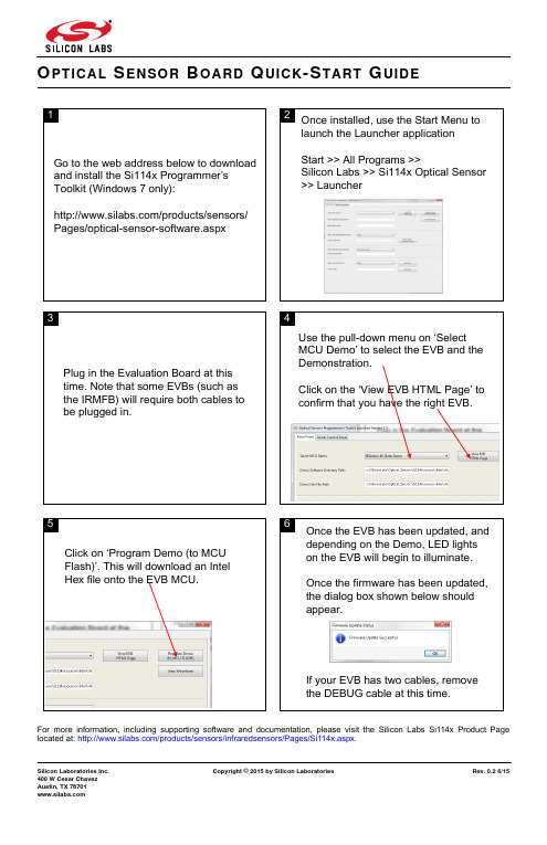
Silicon Laboratories Inc.Copyright © 2015 by Silicon Laboratories Rev. 0.2 6/15400 W Cesar Chavez Austin, TX 78701O PTICAL S ENSOR B OARD Q UICK -S TART G UIDEFor more information, including supporting software and documentation, please visit the Silicon Labs Si114x Product Page located at: /products/sensors/infraredsensors/Pages/Si114x.aspx .6Once the EVB has been updated, and depending on the Demo, LED lights on the EVB will begin to illuminate.If your EVB has two cables, removeFor more information, including supporting software and documentation, please visit the Silicon Labs Si114x Product Page located at: /products/sensors/infraredsensors/Pages/Si114x.aspx .Source Code for the demo can beexamined through ‘Select and View MCU 9It is possible to choose different HEX files more suitable for outdoor use. The ‘Search’ option allows you to choose other HEX files outside the project also.It is also possible to go to source directoryOnce the choice is made, click ‘Flash EVB’EVB’For more information, including supporting software and documentation, please visit the Silicon Labs Si114x Product Page located at: /products/sensors/infraredsensors/Pages/Si114x.aspx .Click on the ‘View Waveform’ button to start Once the waveform begins, you canclick on the Pause button to pause.Once ‘View Waveform’ is started, a file c:\SiliconLabs\Optical_Sensors\Si114x\executable\launcher\output.csv is generated so that the samples can be examined using a text editor。
SI-30 chinese manual

! 注意!!!
本中文操作说明书是由英文原版翻译而成,仅供用户参考,详情请参 阅随机英文原版说明书;
因生产商对设备更改而使说明书与实际操作造成的差异,恕不另行通 知。
பைடு நூலகம்广州市一帆船务设备有限公司
2
自动识别系统 SI-30 中文操作说明书
目
录
1. 缩写.....................................................................................................................................5 2. 概要.....................................................................................................................................5
2.1.1. 主要信息 ........................................................................................
Si446x中文API文档
0X10 FUNC_INFO
0x11 SET_PROPERTY
0X12 GET_PROPERTY
0X13 GPIO_PIN_CFG
0X15 FIFO_INFO
0X20 GET_INT_STATUS
0X33 REQUEST_DEVICE_STATE 0X34 CHANGE_STATE 0×44 READ_CMD_BUFF 0x50 FRR_A_READ 0X51 FRR_B_READ 0x53 FRR_C_READ 0x57 FRR_D_READ
PKT_RX_FIELD_2_LENGTH 0X26 0X27 PKT_RX_FIELD_2_CONFIG 为0x28 PKT_RX_FIELD_2_CRC_CONFIG 0X29
PKT_RX_FIELD_3_LENGTH 0X2A 0x2B中 PKT_RX_FIELD_3_CONFIG 0X2C PKT_RX_FIELD_3_CRC_CONFIG 0X2D PKT_RX_FIELD_4_LENGTH 0X2E
0X18 PROTOCOL_CFG
0X21 GET_PH_STATUS
0x23 GET_CHIP_STATUS
写入数据字节(s)到TX FIFO。 RX_COMMANDS 简介
返回最后接收到的数据包有关的变量字段的长度信息,以及(可选)覆盖字段 的长度。 返回调制解调器中断组(包括状态和暂挂)的中断状态。任选地,它可以被用 来清除锁存(待定)中断事件。 切换到RX状态,并开始数据包的接收。 手动跳变到一个新的频率,而在RX模式。 从RX FIFO中读取数据字节(s)。
组 0X20 0X20
数
名称
0x00 MODEM_MOD_TYPE
0X01 MODEM_MAP_CONTROL
Si4438中文数据手册
修订版 1.0 版权所有 © 2014 Silicon LaboratoriesSi4438-C特点应用说明Silicon Laboratories 的Si4438为高性能的低电流收发器,可覆盖从425至 525MHz 的次千兆赫频段。
Si4438 针对中国智能仪表市场,特别适合于智能电表。
该设备的覆盖区及引脚与 Si446x 无线电兼容,可为全世界的次千兆赫应用提供行业领先的性能。
无线电设备是 EZRadioPRO ®产品系列的一部分,包括全套发射器、接收器和收发器的产品线,涵盖各种应用。
所有零件都具有杰出的灵敏度—124dBm ,可同时实现极低的有效电流和待机电流消耗。
12.5kHz 通道 58dB 相邻通道选择性的间距确保了严苛 RF 条件下的可靠接收操作。
Si4438 可提供超常的高达 +20dBm 具有显著 TX 效率的输出功率。
高输出功率和灵敏度实现了业界领先的144dB 链路预算,实现了范围扩展和高度可靠的通信链路。
⏹频率范围=425–525MHz ⏹接收灵敏度=–124dBm ⏹调制● (G)FSK ● OOK⏹最大输出功率● +20dBm⏹低活动功耗● 14mA RX⏹超低电流断电模式● 30nA 关机,40nA 待机⏹数据传输率=100 bps 到 500kbps⏹前导探测模式● 6在 1.2kbps 时 mA 平均 Rx 电流⏹快速唤醒和跳数⏹电源=1.8 至 3.8V⏹出色的选择性能● 58dB 相邻通道● 1MHz 处阻断增益为 75dB⏹天线分集和 T/R 开关控制⏹高度可配置的分组处理程序⏹TX 和 RX64 字节 FIFO⏹自动频率控制 (AFC)⏹自动增益控制 (AGC)⏹低 BOM⏹低电量探测器⏹温度传感器⏹20 引脚 QFN 封装⏹IEEE 802.15.4g 就绪⏹适合中国调控(国家电网)⏹中国智能仪表专利申请中Si4438-C功能框图Product Freq. Range Max Output Power TX Current RX Current Si4438425–525MHz+20dBm75mA13.7mASi4438-C修订版 1.03目录章节页码1. 电气规格 . . . . . . . . . . . . . . . . . . . . . . . . . . . . . . . . . . . . . . . . . . . . . . . . . . . . . . . . . . . . . . . . .42. 功能描述 . . . . . . . . . . . . . . . . . . . . . . . . . . . . . . . . . . . . . . . . . . . . . . . . . . . . . . . . . . . . . . . .113. 控制器接口 . . . . . . . . . . . . . . . . . . . . . . . . . . . . . . . . . . . . . . . . . . . . . . . . . . . . . . . . . . . . . .123.1. 串行外围接口 (SPI) . . . . . . . . . . . . . . . . . . . . . . . . . . . . . . . . . . . . . . . . . . . . . . . . . .123.2. 快速响应寄存器 . . . . . . . . . . . . . . . . . . . . . . . . . . . . . . . . . . . . . . . . . . . . . . . . . . . . .143.3. 工作模式和计时 . . . . . . . . . . . . . . . . . . . . . . . . . . . . . . . . . . . . . . . . . . . . . . . . . . . . .143.4. 应用程序编程接口 . . . . . . . . . . . . . . . . . . . . . . . . . . . . . . . . . . . . . . . . . . . . . . . . . . .183.5. 中断 . . . . . . . . . . . . . . . . . . . . . . . . . . . . . . . . . . . . . . . . . . . . . . . . . . . . . . . . . . . . . .183.6. GPIO . . . . . . . . . . . . . . . . . . . . . . . . . . . . . . . . . . . . . . . . . . . . . . . . . . . . . . . . . . . . .184. 调制和硬件配置选项 . . . . . . . . . . . . . . . . . . . . . . . . . . . . . . . . . . . . . . . . . . . . . . . . . . . . . . .194.1. 调制类型 . . . . . . . . . . . . . . . . . . . . . . . . . . . . . . . . . . . . . . . . . . . . . . . . . . . . . . . . . .194.2. 硬件配置选项 . . . . . . . . . . . . . . . . . . . . . . . . . . . . . . . . . . . . . . . . . . . . . . . . . . . . . . .194.3. 前导长度 . . . . . . . . . . . . . . . . . . . . . . . . . . . . . . . . . . . . . . . . . . . . . . . . . . . . . . . . . .215. 内部功能块 . . . . . . . . . . . . . . . . . . . . . . . . . . . . . . . . . . . . . . . . . . . . . . . . . . . . . . . . . . . . . .235.1. RX 链 . . . . . . . . . . . . . . . . . . . . . . . . . . . . . . . . . . . . . . . . . . . . . . . . . . . . . . . . . . . . .235.2. RX 调制解调器 . . . . . . . . . . . . . . . . . . . . . . . . . . . . . . . . . . . . . . . . . . . . . . . . . . . . .235.3. 合成器 . . . . . . . . . . . . . . . . . . . . . . . . . . . . . . . . . . . . . . . . . . . . . . . . . . . . . . . . . . . .255.4. 发送器(TX ) . . . . . . . . . . . . . . . . . . . . . . . . . . . . . . . . . . . . . . . . . . . . . . . . . . . . . .275.5. 晶体振荡器 . . . . . . . . . . . . . . . . . . . . . . . . . . . . . . . . . . . . . . . . . . . . . . . . . . . . . . . .296. 数据处理和分组处理程序 . . . . . . . . . . . . . . . . . . . . . . . . . . . . . . . . . . . . . . . . . . . . . . . . . . .316.1. RX 和 TX FIFO . . . . . . . . . . . . . . . . . . . . . . . . . . . . . . . . . . . . . . . . . . . . . . . . . . . . .316.2. 分组处理程序 . . . . . . . . . . . . . . . . . . . . . . . . . . . . . . . . . . . . . . . . . . . . . . . . . . . . . . .327. RX 调制解调器配置 . . . . . . . . . . . . . . . . . . . . . . . . . . . . . . . . . . . . . . . . . . . . . . . . . . . . . . .338. 辅助块 . . . . . . . . . . . . . . . . . . . . . . . . . . . . . . . . . . . . . . . . . . . . . . . . . . . . . . . . . . . . . . . . . .338.1. 唤醒定时器和 32kHz 时钟源 . . . . . . . . . . . . . . . . . . . . . . . . . . . . . . . . . . . . . . . . . . .338.2. 低占空比模式(自动 RX 唤醒) . . . . . . . . . . . . . . . . . . . . . . . . . . . . . . . . . . . . . . . .338.3. 温度、电池电压和辅助 ADC . . . . . . . . . . . . . . . . . . . . . . . . . . . . . . . . . . . . . . . . . . .348.4. 低电量探测器 . . . . . . . . . . . . . . . . . . . . . . . . . . . . . . . . . . . . . . . . . . . . . . . . . . . . . . .358.5. 天线分集 . . . . . . . . . . . . . . . . . . . . . . . . . . . . . . . . . . . . . . . . . . . . . . . . . . . . . . . . . .358.6. 前导探测模式 . . . . . . . . . . . . . . . . . . . . . . . . . . . . . . . . . . . . . . . . . . . . . . . . . . . . . . .359. 引脚描述:Si4438-C . . . . . . . . . . . . . . . . . . . . . . . . . . . . . . . . . . . . . . . . . . . . . . . . . . . . . .3710. 订购信息 . . . . . . . . . . . . . . . . . . . . . . . . . . . . . . . . . . . . . . . . . . . . . . . . . . . . . . . . . . . . . . .3911. 封装外形:Si4438 . . . . . . . . . . . . . . . . . . . . . . . . . . . . . . . . . . . . . . . . . . . . . . . . . . . . . . .4012. PCB 焊盘图案:Si4438 . . . . . . . . . . . . . . . . . . . . . . . . . . . . . . . . . . . . . . . . . . . . . . . . . . .4113. 顶部标记 . . . . . . . . . . . . . . . . . . . . . . . . . . . . . . . . . . . . . . . . . . . . . . . . . . . . . . . . . . . . . . .4313.1. Si4438 顶部标记 . . . . . . . . . . . . . . . . . . . . . . . . . . . . . . . . . . . . . . . . . . . . . . . . . . .4313.2. 顶部标记说明 . . . . . . . . . . . . . . . . . . . . . . . . . . . . . . . . . . . . . . . . . . . . . . . . . . . . . .43联系信息 . . . . . . . . . . . . . . . . . . . . . . . . . . . . . . . . . . . . . . . . . . . . . . . . . . . . . . . . . . . . . . . . . .44Si4438-C1. 电气规格Table 1. DC Characteristics *Parameter Symbol Test ConditionMin Typ Max Unit Supply Voltage RangeV DD 1.8 3.3 3.8V Power Saving ModesI Shutdown RC Oscillator, Main Digital Regulator, and Low Power Digital Regulator OFF —30—nA I Standby Register values maintained and RCoscillator/WUT OFF —40—nA I SleepRC RC Oscillator/WUT ON and all register valuesmaintained, and all other blocks OFF —740—nA I SleepXO Sleep current using an external 32kHz crystal.— 1.7—µA I Sensor -LBD Low battery detector ON, register values maintained, and all other blocks OFF —1—µA I ReadyCrystal Oscillator and Main Digital Regulator ON,all other blocks OFF— 1.8—mA Preamble Sense Mode CurrentI psm Duty cycling during preamble search,1.2kbps, 4 byte preamble —6—mA I psmFixed 1s wakeup interval, 50kbps, 5 bytepreamble—10—µA TUNE Mode Current I Tune_RX RX Tune —7.6—mA I Tune_TX TX Tune —7.8—mA RX Mode Current I RXH —13.7—mA TX Mode Current (Si4438)I TX_+20+20dBm output power, class-E match, 490MHz,3.3V—75—mA*Note: All minimum and maximum values are guaranteed across the recommended operating conditions of supply voltageand from –40 to +85°C unless otherwise stated. All typical values apply at VDD =3.3V and 25°C unless otherwise stated.Si4438-CTable 2. Synthesizer AC Electrical Characteristics1Parameter Symbol Test Condition Min Typ Max UnitF SYN425—525MHz Synthesizer FrequencyRange (Si4438)F RES-525425–525MHz—14.3—Hz Synthesizer FrequencyResolution2—50—µs Synthesizer Settling Time t LOCK Measured from exiting Ready mode withXOSC running to any frequency.Including VCO Calibration.Phase Noise Lφ(f M)∆F=10kHz, 460MHz—–109—dBc/Hz∆F=100kHz, 460MHz—–111—dBc/Hz∆F=1MHz, 460MHz—–131—dBc/Hz∆F=10MHz, 460MHz—–141—dBc/HzNotes:1.All minimum and maximum values are guaranteed across the recommended operating conditions of supply voltage andfrom –40 to +85°C unless otherwise stated. All typical values apply at VDD=3.3V and 25°C unless otherwise stated.2. Default API setting for modulation deviation resolution is double the typical value specified.Si4438-CTable 3. Receiver AC Electrical Characteristics 1ParameterSymbol Test ConditionMin Typ Max Unit RX Frequency Range (Si4438)F RX 425—525MHz RX Sensitivity 2P RX_0.5(BER < 0.1%)(500bps, GFSK, BT =0.5,∆f =±250Hz)2—–124—dBmP RX_40(BER < 0.1%)(40kbps, GFSK, BT =0.5,∆f =±20kHz)2—–108—dBmP RX_100(BER < 0.1%)(100kbps, GFSK, BT =0.5,∆f =±50kHz)1—–104—dBmP RX_9.6(BER < 0.1%)(9.6kbps, GFSK, BT =0.5,∆f =±4.8kHz)2—–114—dBmP RX_OOK(BER < 0.1%, 4.8kbps, 350kHz BW,OOK, PN15 data)2—–108—dBm (BER < 0.1%, 40kbps, 350kHz BW,OOK, PN15 data)2—–102—dBm (BER < 0.1%, 120kbps, 350kHz BW,OOK, PN15 data)2—–98—dBm RX Channel Bandwidth BW 1.1—850kHz RSSI Resolution RES RSSI —±0.5—dB ±1-Ch Offset Selectivity, 450MHz 2C/I 1-CHDesired Ref Signal 3dB above sensitivity, BER < 0.1%. Interferer is CW, and desired is modulated with2.4kbps∆F =1.2kHz GFSK with BT =0.5, RXchannel BW =4.8kHz, channel spacing =12.5kHz —–60—dBBlocking 1MHz Offset 21M BLOCK Desired Ref Signal 3dB above sensitivity, BER =0.1%. Interferer is CW, and desired is modulated with2.4kbps,∆F =1.2kHz GFSK with BT =0.5,RX channel BW =4.8kHz —–77—dB Blocking 8MHz Offset 28M BLOCK—–84—dBImage RejectionIm REJRejection at the image frequency.IF =468kHz—40—dBNotes:1.All minimum and maximum values are guaranteed across the recommended operating conditions of supply voltage andfrom –40 to +85°C unless otherwise stated. All typical values apply at VDD =3.3V and 25°C unless otherwise stated.2. Measured over 50000 bits using PN9 data sequence and data and clock on GPIOs. Sensitivity is expected to be betterif reading data from packet handler FIFO especially at higher data rates.Si4438-CTable 4. Transmitter AC Electrical Characteristics1Parameter Symbol Test Condition Min Typ Max Unit TX FrequencyRangeF TX425—525MHz(G)FSK Data Rate2DR FSK0.1—500kbps OOK Data Rate2DR OOK0.1—120kbps Modulation DeviationRange∆f525425–525MHz—750—kHz Modulation DeviationResolution3F RES-525425–525MHz—14.3—HzOutput Power Range4P TXTypical range at 3.3Vwith class E match optimized for bestPA efficiency.–20—+20dBmTX RF Output Steps∆PRF_OUT Using Class E match within 6dB of maxpower—0.25—dBTX RF Output LevelVariation vs. Temperature∆P RF_TEMP–40 to +85︒C— 2.3—dB TX RF Output LevelVariation vs. Frequency∆P RF_FREQ—0.6—dBTransmit ModulationFiltering B*T Gaussian Filtering Bandwith TimeProduct—0.5—Notes:1.All minimum and maximum values are guaranteed across the recommended operating conditions of supply voltage andfrom –40 to +85°C unless otherwise stated. All typical values apply at VDD=3.3V and 25 °C unless otherwise stated.2. The maximum data rate is dependent on the XTAL frequency and is calculated as per the formula:Maximum Symbol Rate=Fxtal/60, where Fxtal is the XTAL frequency (typically 30MHz).3. Default API setting for modulation deviation resolution is double the typical value specified.4. Output power is dependent on matching components and board layout.Si4438-CTable 5. Auxiliary Block Specifications 1ParameterSymbol Test ConditionMin Typ Max Unit Temperature Sensor SensitivityTS S—4.5—ADC Codes/°C Low Battery Detector ResolutionLBD RES —50—mV Microcontroller ClockOutput Frequency Range 2F MCConfigurable to Fxtal or Fxtal divided by 2, 3, 7.5, 10, 15, or 30 where Fxtal is the reference XTAL frequency. In addition, 32.768kHz is also supported.32.768K—FxtalHzTemperature Sensor Conversion TEMP CT Programmable setting—3—ms XTAL Range 3XTAL Range25—32MHz 30MHz XTAL Start-Up Timet 30MUsing XTAL and board layout in reference design. Start-up time will vary with XTAL type andboard layout.—300—µs30MHz XTAL Cap Resolution30M RES —70—fF 32kHz XTAL Start-Up Time t 32k —2—sec 32kHz Accuracy using Internal RC Oscillator 32KRC RES—2500—ppm POR Reset Timet POR——6msNotes:1.All minimum and maximum values are guaranteed across the recommended operating conditions of supply voltage andfrom –40 to +85°C unless otherwise stated. All typical values apply at V DD =3.3V and 25°C unless otherwise stated.2. Microcontroller clock frequency tested in production at 1MHz, 30MHz, 32MHz, and 32.768kHz. Other frequenciestested in bench characterization.3. XTAL Range tested in production using an external clock source (similar to using a TCXO).Si4438-CTable 6. Digital IO Specifications (GPIO_x, SCLK, SDO, SDI, nSEL, nIRQ, SDN)1Parameter Symbol Test Condition Min Typ Max Unit Rise Time2,3T RISE0.1x V DD to 0.9x V DD,C L=10pF,DRV<1:0>=LL— 2.3—nsFall Time3,4T FALL0.9x V DD to 0.1x V DD,C L=10pF,DRV<1:0>=LL—2—nsInput Capacitance C IN—2—pF Logic High Level Input Voltage V IH V DD x0.7——V Logic Low Level Input Voltage V IL——V DD x0.3V Input Current I IN0<V IN< V DD–1—1µA Input Current If Pullup is Activated I INP V IL=0V1—4µADrive Strength for Output Low Level I OmaxLL DRV[1:0]=LL3— 6.66—mA I OmaxLH DRV[1:0]=LH3— 5.03—mA I OmaxHL DRV[1:0]=HL3— 3.16—mA I OmaxHH DRV[1:0]=HH3— 1.13—mADrive Strength for Output High Level I OmaxLL DRV[1:0]=LL3— 5.75—mA I OmaxLH DRV[1:0]=LH3— 4.37—mA I OmaxHL DRV[1:0]=HL3— 2.73—mA I OmaxHH DRV[1:0]=HH3—0.96—mADrive Strength for Output High Level for GPIO0I OmaxLL DRV[1:0]=LL3— 2.53—mA I OmaxLH DRV[1:0]=LH3— 2.21—mA I OmaxHL DRV[1:0]=HL3— 1.7—mA I OmaxHH DRV[1:0]=HH3—0.80—mALogic High Level Output Voltage V OH DRV[1:0]=HL V DD x0.8——V Logic Low Level Output Voltage V OL DRV[1:0]=HL——V DD x0.2V Notes:1.All minimum and maximum values are guaranteed across the recommended operating conditions of supply voltageand from –40 to +85°C unless otherwise stated. All typical values apply at V DD=3.3V and 25°C unless otherwise stated.2. 6.7ns is typical for GPIO0 rise time.3. Assuming VDD=3.3V, drive strength is specified at Voh (min)=2.64V and Vol(max)=0.66V at room temperature.4. 2.4ns is typical for GPIO0 fall time.Si4438-CTable 7. Thermal Operating CharacteristicsParameterValue Unit Operating Ambient Temperature Range T A –40 to +85︒C Thermal Impedance θJA 25︒C /W Junction Temperature T JMAX +105︒C Storage Temperature Range T STG–55 to +150︒CTable 8. Absolute Maximum Ratings*ParameterValue Unit V DD to GND–0.3, +3.8V Instantaneous V RF-peak to GND on TX Output Pin –0.3, +8.0V Sustained V RF-peak to GND on TX Output Pin –0.3, +6.5V Voltage on Digital Control Inputs –0.3, V DD + 0.3 V Voltage on Analog Inputs–0.3, V DD + 0.3V Voltage on XIN Input when using a TCXO –0.7, V DD + 0.3V RX Input Power+10dBm*Note: Stresses beyond those listed under “Absolute Maximum Ratings” may cause permanent damage to the device. Theseare stress ratings only and functional operation of the device at or beyond these ratings in the operational sections of the specifications is not implied. Exposure to absolute maximum rating conditions for extended periods may affect device reliability. Power Amplifier may be damaged if switched on without proper load or termination connected. TX matching network design will influence TX V RF-peak on TX output pin. Caution: ESD sensitive device.2. 功能描述Si4438 设备为高性能低电流的无线 ISM 收发器,可覆盖次千兆赫波段。
- 1、下载文档前请自行甄别文档内容的完整性,平台不提供额外的编辑、内容补充、找答案等附加服务。
- 2、"仅部分预览"的文档,不可在线预览部分如存在完整性等问题,可反馈申请退款(可完整预览的文档不适用该条件!)。
- 3、如文档侵犯您的权益,请联系客服反馈,我们会尽快为您处理(人工客服工作时间:9:00-18:30)。
说明
阀门控制 烟雾探测器 非接触开关 非接触滑动器 占位传感器 消费类电子设备 工业自动化 显示屏背光控制 光中断器
Si1141/42/43 是基于反射的低功率红外线临近和环境光传感器,带有 I2C 数字接口和 可编程事件中断输出。此非接触传感器 IC 包括模拟到数字转换器、集成高灵敏度可 见和红外线光电二极管 、数字信号处理器和具有十五个可选驱动电平的一个、两个或 三个集成红外线 LED 驱动器。Si1141/42/43 在广泛的动态范围和包括阳光直射在内 的各种光源下可提供优异性能。Si1141/42/43 还可以在深色玻璃盖下工作。光电二极 管响应和关联的数字转换电路对人造光闪烁噪声和自然光颤动噪声具有优异的抗扰 性。Si1142/43 具有两个或多个 LED,能够支持多轴式临近运动探测。Si1141/42/43 器件 在 10 引 线 2x2 mm QFN 封装 中提 供,能够 在 –40 至 +85 °C 温 度 范围 中在 1.71 至 3.6 V 的条件下运行。
Regulator
Temp A M U
Visible
X
Infrared
ADC
Filter
LED Drivers
Digital Sequencer & Control Logic
I2C
Registers
Oscillator
LED1 LED21 LED32
GND
1. Si1142 and Si1143 only. 2. Si1143 only.
每个 LED 驱动器有 15 个电流 设置,从 5.6 mA 到 360 mA
25.6 µs LED 驱动器脉冲宽度 50 cm 临近范围,具有单个脉冲
(<3 klx)
扰度 业界最低的功耗
1.71 至 3.6 V 电源电压 9 µA 平均电流 (180 mA 和 3 µA
Si114x 电源时每 800 ms LED 脉冲
Pin Assignments
SDA SCL VDD INT
DNC
10
1
9
2
8
QFN-10
3
7
4
6
5
DNC
LED1 GND LED3 LED2
Rev. 1.3 5/12
版权 © 2011 Silicon Laboratories
Si1141/42/43
Si1141/42/43
功能框图
VDD
INT SCL SDA
在两个 ADC 范围设置之间动态 范围可以达到 1 至 128 klx
内置电压电源监控器和接通电源复 位控制器
串行通信 数据速率高达 3.4 Mbps
从模式硬件地址解码 小外形 10 引线 2x2 mm QFN 温度范围
–40 至 +85 °C
应用
手机 电子书阅读器 笔记本 / 上网本 便携式消费类电子设备 音频产品 安全面板 窜改探测电路 分配器
4. 编程指南 . . . . . . . . . . . . . . . . . . . . . . . . . . . . . . . . . . . . . . . . . . . . . . . . . . . . . . . . . . . . . . . . 19 4.1. 命令和响应结构 . . . . . . . . . . . . . . . . . . . . . . . . . . . . . . . . . . . . . . . . . . . . . . . . . . . . . 19 4.2. 命令协议 . . . . . . . . . . . . . . . . . . . . . . . . . . . . . . . . . . . . . . . . . . . . . . . . . . . . . . . . . . 20 4.3. 资源汇总 . . . . . . . . . . . . . . . . . . . . . . . . . . . . . . . . . . . . . . . . . . . . . . . . . . . . . . . . . . 22 4.4. 信号通路软件模型 . . . . . . . . . . . . . . . . . . . . . . . . . . . . . . . . . . . . . . . . . . . . . . . . . . . 27 4.5. I2C 寄存器 . . . . . . . . . . . . . . . . . . . . . . . . . . . . . . . . . . . . . . . . . . . . . . . . . . . . . . . . . 28 4.6. 参数 RAM . . . . . . . . . . . . . . . . . . . . . . . . . . . . . . . . . . . . . . . . . . . . . . . . . . . . . . . . . 52
3.3 V
Host SDA SCL
INT
0.1 uF
Si1141
SDA
LED1
SCL
GND
VDD CVDD
INT CVDD
30 ohm 5%, 1/16 W
15 µF, 20%, >6 V
3.3 V Host
Figure 1. Si1141 Basic Application
4.3 V
No Pop
Si1143
SDA
LED1
SCL
GND
VDD
LED3
INT
LED2
0.1 uF
30 ohm 5%, 1/16 W
22 uF, 20%, >6V
Figure 2. Si1143 Application with Three LEDs and Separate LED Power Supply
注: 有关更多的应用示例,请参阅 “AN498:Si114x 临近应用的 irLED 选择指南 ”。
Si1141/42/43
带 I2C 接口的临近 / 环境光传感器 IC
功能
QuickSense™ 集成红外线临近探测器 使用红外校正算法可以准确测量照
临近探测可从 1 cm 以下调节到超过
明度
50 cm
25.6µs LED “ 开启 ” 时间使总功
三个独立的 LED 驱动器
耗占空比较低,不会影响性能和抗
3. 运行模式 . . . . . . . . . . . . . . . . . . . . . . . . . . . . . . . . . . . . . . . . . . . . . . . . . . . . . . . . . . . . . . . . 17 3.1. 关闭模式 . . . . . . . . . . . . . . . . . . . . . . . . . . . . . . . . . . . . . . . . . . . . . . . . . . . . . . . . . . 17 3.2. 初始化模式 . . . . . . . . . . . . . . . . . . . . . . . . . . . . . . . . . . . . . . . . . . . . . . . . . . . . . . . . 17 3.3. 备用模式 . . . . . . . . . . . . . . . . . . . . . . . . . . . . . . . . . . . . . . . . . . . . . . . . . . . . . . . . . . 17 3.4. 强制转换模式 . . . . . . . . . . . . . . . . . . . . . . . . . . . . . . . . . . . . . . . . . . . . . . . . . . . . . . . 17 3.5. 自发运行模式 . . . . . . . . . . . . . . . . . . . . . . . . . . . . . . . . . . . . . . . . . . . . . . . . . . . . . . . 18
15 cm 临近范围,具有单个脉冲 (>3 klx)
25.6 µs) < 500 nA 待机电流
运行时高达 128 klx (阳光直射)
支持内部和外部唤醒
高反射灵敏度 < 1 µW/cm2
高电磁抗扰性,无屏蔽封装 QuickSense™ 集成环境光传感器