01253759.4半导体放电管半导体芯片
600v的半导体放电管

600v的半导体放电管600V的半导体放电管在现代电子技术中扮演着重要的角色。
它是一种能够在高压环境下实现电流控制的器件,具有很多应用领域。
在本文中,我们将探索半导体放电管的工作原理、特性以及应用。
半导体放电管是一种半导体器件,能够在电压超过一定阈值时产生放电现象。
这种器件通常由多个半导体材料层叠而成,其中包含N 型和P型硅等材料。
当电压施加到半导体放电管上时,电子和空穴会在半导体材料中产生,并形成电流。
当电压超过一定阈值时,半导体放电管中的电子和空穴会发生复合,产生能量释放,从而引发放电现象。
半导体放电管的特性使得它在许多领域得到了广泛应用。
首先,它可以用作电子开关,因为它能够在开关状态间快速切换。
这使得它在电力系统中的保护装置中得到了广泛应用,可以有效地防止电流过载和短路等故障。
其次,半导体放电管还可以用于电磁干扰的抑制。
它可以通过在电路中引入一个阻抗,将电磁干扰分散或吸收,从而减少电子设备之间的干扰。
此外,半导体放电管还可以用于光电子器件和激光器等高科技领域。
除了以上应用外,半导体放电管还可以用于电力电子转换器、医疗设备、通信设备等领域。
它的小体积、高效率和可靠性使得它成为了现代电子技术中不可或缺的一部分。
尽管半导体放电管在电子技术中起着重要的作用,但它也存在一些局限性。
首先,它的工作电压范围相对有限,通常在几百伏特至几千伏特之间。
其次,半导体放电管对温度变化非常敏感,过高或过低的温度都可能影响其性能。
此外,半导体放电管还存在寿命限制,长时间使用后可能出现性能下降或故障。
600V的半导体放电管是一种重要的半导体器件,具有广泛的应用领域。
它的工作原理和特性使得它成为现代电子技术中不可或缺的一部分。
然而,它也存在一些局限性,需要在实际应用中加以考虑。
通过深入了解半导体放电管的工作原理和应用,我们可以更好地利用它的优点,为现代电子技术的发展做出贡献。
芯片封装类型图鉴
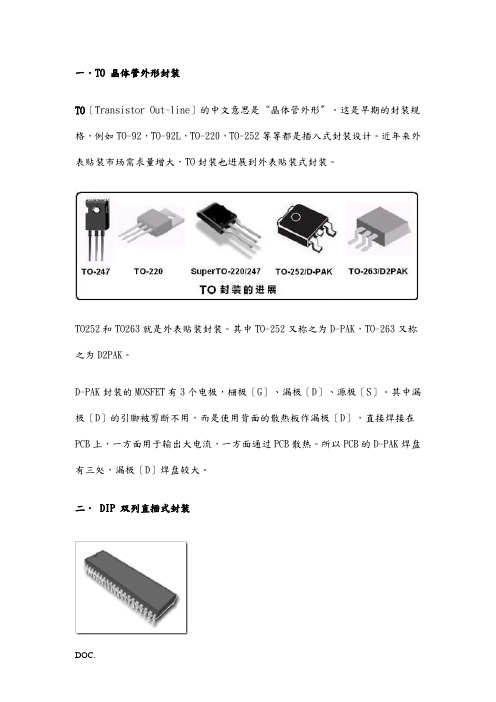
一.TO 晶体管外形封装TO〔Transistor Out-line〕的中文意思是“晶体管外形〞。
这是早期的封装规格,例如TO-92,TO-92L,TO-220,TO-252等等都是插入式封装设计。
近年来外表贴装市场需求量增大,TO封装也进展到外表贴装式封装。
TO252和TO263就是外表贴装封装。
其中TO-252又称之为D-PAK,TO-263又称之为D2PAK。
D-PAK封装的MOSFET有3个电极,栅极〔G〕、漏极〔D〕、源极〔S〕。
其中漏极〔D〕的引脚被剪断不用,而是使用背面的散热板作漏极〔D〕,直接焊接在PCB上,一方面用于输出大电流,一方面通过PCB散热。
所以PCB的D-PAK焊盘有三处,漏极〔D〕焊盘较大。
二. DIP 双列直插式封装DIP(DualIn-line Package)是指采用双列直插形式封装的集成电路芯片,绝大多数中小规模集成电路(IC)均采用这种封装形式,其引脚数一般不超过100个。
封装材料有塑料和陶瓷两种。
采用DIP封装的CPU芯片有两排引脚,使用时,需要插入到具有DIP结构的芯片插座上。
当然,也可以直接插在有一样焊孔数和几何排列的电路板上进展焊接。
DIP封装结构形式有:多层陶瓷双列直插式DIP,单层陶瓷双列直插式DIP,引线框架式DIP〔含玻璃陶瓷封接式,塑料包封结构式,陶瓷低熔玻璃封装式〕等。
DIP封装具有以下特点:1.适合在PCB (印刷电路板)上穿孔焊接,操作方便。
2.比TO型封装易于对PCB布线。
3.芯片面积与封装面积之间的比值较大,故体积也较大。
以采用40根I/O引脚塑料双列直插式封装(PDIP)的CPU为例,其芯片面积/封装面积=(3×3)/(15.24×50)=1:86,离1相差很远。
〔PS:衡量一个芯片封装技术先进与否的重要指标是芯片面积与封装面积之比,这个比值越接近1越好。
如果封装尺寸远比芯片大,说明封装效率很低,占去了很多有效安装面积。
XB5352G 贴片SOT23-5 单节锂电池充电保护芯片 电源管理IC
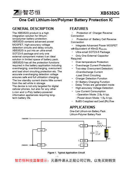
XB5352G ____________________________________________________________________________________________________________________________ One Cell Lithium-ion/Polymer Battery Protection ICGENERAL DESCRIPTIONThe XB5352G product is a high integration solution for lithium-ion/polymer battery protection.XB5352G contains advanced power MOSFET, high-accuracy voltage detection circuits and delay circuits.XB5352G is put into an ultra-smallSOT23-5 package and only oneexternal component makes it an ideal solution in limited space of battery pack. XB5352G has all the protection functions required in the battery application including overcharging, overdischarging, overcurrent and load short circuiting protection etc. The accurate overcharging detection voltage ensures safe and full utilization charging. The low standby current drains little current from the cell while in storage.The device is not only targeted for digital cellular phones, but also for any otherLi-Ion and Li-Poly battery-powered information appliances requiring long-term battery life. FEATURES·Protection of Charger Reverse Connection·Protection of Battery Cell Reverse Connection·Integrate Advanced Power MOSFET with Equivalent of 45mΩ R SS(ON)·Ultra-small SOT23-5 Package ·Only One External Capacitor Required·Over-temperature Protection ·Overcharge Current Protection ·Two-step Overcurrent Detection: -Overdischarge Current-Load Short Circuiting·Charger Detection Function·0V Battery Charging Function- Delay Times are generated inside ·High-accuracy Voltage Detection ·Low Current Consumption- Operation Mode: 2.8μA typ.- Power-down Mode: 1.5μA typ. ·RoHS Compliant and Lead (Pb) FreeAPPLICATIONSOne-Cell Lithium-ion Battery PackLithium-Polymer Battery PackFigure 1. Typical Application CircuitORDERING INFORMATIONNote: “YW” is manufacture date code, “Y” means the year, “W” means the weekPIN CONFIGURATIONFigure 2. PIN ConfigurationPIN DESCRIPTIONABSOLUTE MAXIMUM RATINGS(Note: Do not exceed these limits to prevent damage to the device. Exposure to absolute maximum rating conditions for long periods may affect device reliability.)ELECTRICAL CHARACTERISTICSTypicals and limits appearing in normal type apply for T A= 25o C, unless otherwise specifiedFigure 3. Functional Block Diagram FUNCTIONAL DESCRIPTIONThe XB5352G monitors the voltage and current of a battery and protects it from being damaged due to overcharge voltage, overdischarge voltage, overdischarge current, and short circuit conditions by disconnecting the battery from the load or charger. These functions are required in order to operate the battery cell within specified limits.The device requires only one external capacitor. The MOSFET is integrated andits R SS(ON) is as low as45mΩtypical. Normal operating modeIf no exception condition is detected, charging and discharging can be carried out freely. This condition is called the normal operating mode.Overcharge ConditionWhen the battery voltage becomes higher than the overcharge detection voltage (V CU) during charging under normal conditionand the state continues for the overcharge detection delay time (t CU) or longer, theXB5352G turns the charging control FEToff to stop charging. This condition is called the overcharge condition. The overcharge condition is released in the following two cases:1, When the battery voltage drops below the overcharge release voltage (V CL), the XB5352G turns the charging control FET on and returns to the normal condition.2, When a load is connected and discharging starts, the XB5352G turns the charging control FET on and returns to the normal condition. The release mechanism is as follows: the discharging current flows through an internal parasitic diode of the charging FET immediately after a load is connected and discharging starts, and the VM pin voltage increases about 0.7 V (forward voltage of the diode) from the GND pin voltage momentarily. TheXB5352G detects this voltage and releases the overcharge condition. Consequently, in the case that the battery voltage is equal to or lower than the overcharge detection voltage (V CU), the XB5352G returns to the normal condition immediately, but in the case the battery voltage is higher than the overcharge detection voltage (V CU),the chip does not return to the normal condition until the battery voltage drops below the overcharge detection voltage (V CU) even if the load is connected. In addition, if the VM pin voltage is equal to or lower than the overcurrent 1 detection voltage when a load is connected and discharging starts, the chip does not return to the normal condition.Remark If the battery is charged to a voltage higher than the overcharge detection voltage (V CU) and the battery voltage does not drops below the overcharge detection voltage (V CU) even when a heavy load, which causes an overcurrent, is connected, the overcurrent 1 and overcurrent 2 do not work until the battery voltage drops below the overcharge detection voltage (V CU). Since an actual battery has, however, an internal impedance of several dozens of mΩ, and the battery voltage drops immediately after a heavy load which causes an overcurrent is connected, the overcurrent 1 and overcurrent 2 work. Detection of load short-circuiting works regardless of the battery voltage.Overdischarge ConditionWhen the battery voltage drops below the overdischarge detection voltage (V DL) during discharging under normal condition and it continues for the overdischarge detection delay time (t DL) or longer, theXB5352G turns the discharging control FET off and stops discharging. This condition is called overdischarge condition. After the discharging control FET is turned off, the VM pin is pulled up by the R VMD resistorbetween VM and VDD in XB5352G. Meanwhile when VM is bigger than 1.5V (typ.) (the load short-circuiting detection voltage), the current of the chip is reduced to the power-down current (I PDN). This condition is called power-down condition. The VM and VDD pins are shorted by theR VMD resistor in the IC under the overdischarge and power-down conditions. The power-down condition is released when a charger is connected and the potential difference between VM and VDD becomes 1.3 V (typ.) or higher (load short-circuiting detection voltage). At this time, the FET is still off. When the battery voltage becomes the overdischarge detection voltage (V DL) or higher (see note), the XB5352G turns the FET on and changes to the normal condition from the overdischarge condition.Remark If the VM pin voltage is no less than the charger detection voltage (V CHA), when the battery under overdischarge condition is connected to a charger, the overdischarge condition is released (the discharging control FET is turned on) as usual, provided that the battery voltage reaches the overdischarge release voltage (V DU) or higher. Overcurrent ConditionWhen the discharging current becomes equal to or higher than a specified value (the VM pin voltage is equal to or higher than the overcurrent detection voltage)during discharging under normal condition and the state continues for the overcurrent detection delay time or longer, theXB5352G turns off the discharging control FET to stop discharging. This condition is called overcurrent condition. (The overcurrentincludes overcurrent, or load short-circuiting.)The VM and GND pins are shorted internally by the R VMS resistor under the overcurrent condition. When a load is connected, the VM pin voltage equals the VDD voltage due to the load.The overcurrent condition returns to the normal condition when the load is released and the impedance between the B+ and B- pins becomes higher than the automatic recoverable impedance. When the load is removed, the VM pin goes back to the GND potential since the VM pin is shorted the GND pin with the R VMS resistor. Detecting that the VM pin potential is lower than the overcurrent detection voltage(V IOV), the IC returns to the normal condition.Abnormal Charge Current DetectionIf the VM pin voltage drops below the charger detection voltage (V CHA) during charging under the normal condition and it continues for the overcharge detection delay time (t CU) or longer, the XB5352G turns the charging control FET off and stops charging. This action is called abnormal charge current detection. Abnormal charge current detection works when the discharging control FET is on and the VM pin voltage drops below the charger detection voltage (V CHA). When an abnormal charge current flows into a battery in the overdischarge condition, the XB5352G consequently turns the charging control FET off and stops charging after the battery voltage becomes the overdischarge detection voltage and the overcharge detection delay time (t CU) elapses.Abnormal charge current detection is released when the voltage difference between VM pin and GND pin becomes lower than the charger detection voltage (V CHA) by separating the charger. Since the 0 V battery charging function has higher priority than the abnormal charge current detection function, abnormal charge current may not be detected by the product with the 0 V battery charging function while the battery voltage is low.Load Short-circuiting conditionIf voltage of VM pin is equal or below short circuiting protection voltage (V SHORT), the XB5352G will stop discharging and battery is disconnected from load. The maximum delay time to switch current off is t SHORT. This status is released when voltage of VM pin is higher than short protection voltage (V SHORT), such as when disconnecting the load.Delay CircuitsThe detection delay time for overdischarge current 2 and load short-circuiting starts when overdischarge current 1 is detected. As soon as overdischarge current 2 or load short-circuiting is detected over detection delay time for overdischarge current 2 or load short- circuiting, the XB5352G stops discharging. When battery voltage falls below overdischarge detection voltage due to overdischarge current, the XB5352G stop discharging by overdischarge current detection. In this case the recovery of battery voltage is so slow that if battery voltage after overdischarge voltage detection delay time is still lower than overdischarge detection voltage, the XB5352G shifts to power-down.Figure 4. Overcurrent delay time0V Battery Charging Function (1) (2) (3) This function enables the charging of a connected battery whose voltage is 0 V by self-discharge. When a charger having 0 V battery start charging charger voltage(V0CHA) or higher is connected between B+ and B- pins, the charging control FET gate is fixed to VDD potential. When the voltage between the gate and the source of the charging control FET becomes equal to or higher than the turn-on voltage by the charger voltage, the charging control FET is turned on to start charging. At this time, the discharging control FET is off and the charging current flows through the internal parasitic diode in the discharging control FET. If the battery voltage becomes equal to or higher than the overdischarge release voltage (V DU), the normal condition returns. Note(1) Some battery providers do not recommend charging of completely discharged batteries. Please refer to battery providers before the selection of 0 V battery charging function.(2) The 0V battery charging function has higher priority than the abnormal charge current detection function. Consequently, a product with the 0 V battery charging function charges a battery and abnormal charge current cannot be detected during the battery voltage is low (at most 1.8 V or lower).(3) When a battery is connected to the IC for the first time, the IC may not enter the normal condition in which discharging is possible. In this case, set the VM pin voltage equal to the GND voltage (short the VM and GND pins or connect a charger) to enter the normal condition.TIMING CHART1.Overcharge and overdischarge detectionV V CU -V V DL +V V DL ONONCHARGEV DDV ov1V SS V VMFigure5-1 Overcharge and Overdischarge Voltage Detection2.Overdischarge current detectionV CU V CU -V HC V DL +V DH V DLONDISCHARGEOFFV DDV V ov2V ov1V SS(1)(4)(1)(1)(1)(4)(4)Figure5-2 Overdischarge Current DetectionRemark: (1) Normal condition (2) Overcharge voltage condition (3) Overdischarge voltage condition (4)Overcurrent condition3.Charger DetectionVV CU-VV DL+VV DLONV DDVMV SSVFigure5-3 Charger Detection4.Abnormal Charger DetectionVV CU-VV DL+VV DLONONCHARGEV DDVMV SSVFigure5-4 Abnormal Charger DetectionRemark: (1) Normal condition (2) Overcharge voltage condition (3) Overdischarge voltage condition (4)Overcurrent conditionTYPICAL CHARACTERISTICS(Test based on XB5352G version, V BAT = 3.6V, T A= 25 C unless otherwise specified)Internal FET On-Resistance vs. Junction TemperatureTYPICAL APPLICATIONAs shown in Figure 6, the bold line is the high density current path which must be kept as short as possible. For thermal management, ensure that these trace widths are adequate. C1 is a decoupling capacitor which should be placed as close as possible to XB5352G.Fig 6 XB5352G in a Typical Battery Protection CircuitPrecautions• Pay attention to the operating conditions for input/output voltage and load current so that the power loss in XB5352G does not exceed the power dissipation of the package.• Do not apply an el ectrostatic discharge to this XB5352G that exceeds the performance ratings of the built-in electrostatic protection circuit.XB5352G______________________________________ ____________________________________________________ ________ _________ ____________ - 11 -PACKAGE OUTLINESOT23-5 PACKAGE OUTLINE AND DIMENSIONS。
半导体放电管SMA

A.General Description 简要概述半导体放电管器件专门用来防止敏感的电信设备、POS 终端、基站设备、网络视频等设备出现由闪电、电源接触和电源感应引起的过压故障危险。
它们具有高电气浪涌抑制能力,有助于防止瞬间故障和断开状态的高阻抗,使系统的正常运行过程变得实际上更加透明。
广泛应用在:网络通迅及消费类电子产品、高速数据传输设备(T1/E1、XDSL、ISDN、HDSL、CATV、SLIC 等)。
经典应用:电话信号接口防护、RS485、RS232、RS422等数据接口。
产品特点产品特点:: 精确导通电压、快速响应 超强的浪涌处理能力 双向对称,可靠性高 安装简便,器件体积小分SMA、SMB 贴片型/DO-15、TO-92直插型 符合ROHS 要求满足通信产品标准要求SMA/DO-214ACB.Dimension产品尺寸D.Surge Ratings 浪涌额定值E.Product Terminology 产品术语Electrical Parameters电气参数V DM :Repetitive peak Off-state Voltage 最高峰值电压,器件可保持关断状态,也即:不正作峰值电压VBo:Switching Voltage半导体雪崩或开关切换动作电压Ipp :Surge Ratings最大额定峰值脉冲电流I DM :Off-state current在V DM 下最大泄漏电流值I H Min :Minimum Holding current 导通状态最小电流C :O ff-state Capacitance 不工作状态下器件电容值di/dt :Rate of Rise of Current 电流上升率dv/dt :Rate of Rise of Voltage电压上升率F.Thermal Considerations温度特性考虑封装形式Symbol符号Parameter参数Value值SMA/Do-214ACT J Operating Junction Temperature Range工作温度范围-40~+150℃T S Storage Temperature Range贮存温度范围-55~+150℃RØJA Thermal Resistance:Junction to Ambient90℃/WG.Part Name Information 产品命名信息H.Packing information 包装信息505000PCS/Reel 00PCS/Reel1010000PCS 000PCS /BOX50,000PCS /CartonNOTE:ALL DATA AND SPECIFICATIONS ARE SUBJECT TO CHANGE WITHOUT NOTICE.注意注意::所有的规格、参数更新将不例行通知。
半导体元器件 hs编码

半导体元器件hs编码
根据2023年12月的最新HS编码(海关编码)标准,半导体元器件的HS编码通常属于以下范畴:
8541.10 半导体集成电路(包括微处理器和控制器)
8541.20 其他具有至少一个电子功能的半导体器件
8541.30 敏感半导体器件,包括光电转换器、光敏电阻和光敏晶体管等
8541.40 晶体管,包括硅晶体管、绝缘栅双极型晶体管(IGBT)和场效应晶体管(FET)等
8541.50 二极管,包括整流二极管、肖特基二极管和发光二极管(LED)等
8541.60 光电管和光电倍增管
8541.70 磁电子器件和磁传感器
8541.90 其他半导体器件,如电容器、电阻器和电感器等
请注意,具体的HS编码可能因国家/地区而异。
建议在使用时参考当地海关或贸易部门的最新编码标准以确保准确性。
1。
硕凯半导体放电管型号大全-改

硕凯半导体放电管型号大全硕凯电子(Sylvia)1、半导体放电管产品简述半导体过压保护器是根据可控硅原理采用离子注入技术生产的一种新型保护器件,具有精确导通、快速响应(响应时间ns级)、浪涌吸收能力较强、双向对称、可靠性高等特点。
由于其浪涌通流能力较同尺寸的TVS管强,可在无源电路中代替TVS管使用。
但它的导通特性接近于短路,不能直接用于有源电路中,在这样的电路中使用时必须加限流元件,使其续流小于最小维持电流。
半导体过压保护器有贴装式、直插式和轴向引线式三种封装形式。
2、半导体放电管型号大全(1)名称:P0080SA-P5000SA(DO-214AA)封装:DO-214AA产品系列:P0080SA-P5000SA规格:P0080SA、P0300SA、P0640SA、P0720SA、P0900SA、P1100SA、P1300SA、P1500SA、P1800SA、P2000 SA、P2300SA、P2600SA、P3100SA、P3500SA、P4000SA、P4500SA、P5000SA(2)名称:P0080SB-P5000SB(DO-214AA)封装:DO-214AA产品系列:P0080SB-P5000SB规格:P0080SB、P0300SB、P0640SB、P0720SB、P0900SB、P1100SB、P1300SB、P1500SB、P1800SB、P2000SB、P2300SB、P2600SB、P3100SB、P3500SB、P4000SB、P4500SB、P5000SB(3)名称:P0080SC-P5000SC(DO-214AA)封装:DO-214AA产品系列:P0080SC-P5000SC规格:P0080SC、P0300SC、P0640SC、P0720SC、P0900SC、P1100SC、P1300SC、P1500SC、P1800SC、P2000SC、P2300SC、P2600SC、P3100SC、P3500SC、P4000SC、P4500SC、P5000SC(4)名称:P0080TA-P5000TA(DO-214AC)封装:DO-214AC产品系列:P0080TA-P5000TA规格:P0080TA、P0300TA、P0640TA、P0720TA、P0900TA、P1100TA、P1300TA、P1500TA、P1800TA、P2000TA、P2300TA、P2600TA、P3100TA、P3500TA、P4000TA、P4500TA、P5000TA(5)名称:P0080EA-P5000EA(TO-92)封装:TO-92产品系列:P0080EA-P5000EA规格:P0080EA、P0300EA、P0640EA、P0720EA、P0900EA、P1100EA、P1300EA、P1500EA、P1800EA、P2000EA、P2300EA、P2600EA、P3100EA、P3500EA、P4000EA、P4500EA、P5000EA(6)名称:P0080EB-P5000EB(TO-92)封装:TO-92产品系列:P0080EB-P5000EB规格:P0080EB、P0300EB、P0640EB、P0720EB、P0900EB、P1100EB、P1300EB、P1500EB、P1800EB、P2000EB、P2300EB、P2600EB、P3100EB、P3500EB、P4000EB、P4500EB、P5000EB、(7)名称:P0080EC-P5000EC(TO-92)封装:TO-92产品系列:P0080EC-P5000EC规格:P0080EC、P0300EC、P0640EC、P0720EC、P0900EC、P1100EC、P1300EC、P1500EC、P1800EC、P2000 EC、P2300EC、P2600EC、P3100EC、P3500EC、P4000EC、P4500EC、P5000EC(8)名称:P0080LA-P5000LA(DO-41)封装:DO-41产品系列:P0080EC-P5000EC规格:P0080LA、P0300LA、P0640LA、P0720LA、P0900LA、P1100LA、P1300LA、P1500LA、P1800LA、、P200 0LA、P2300LA、P2600LA、P3100LA、P3500LA、P4000LA、P4500LA、P5000LA(9)名称:P0080LB-P5000LB(DO-15)封装:DO-15产品系列:P0080LB-P5000LB规格:P0080LB、P0300LB、P0640LB、P0720LB、P0900LB、P1100LB、P1300LB、P1500LB、P1800LB、P2000 LB、P2300LB、P2600LB、P3100LB、P3500LB、P4000LB、P4500LB、P5000LB(10)名称:P0080LC-P5000LC(DO-27)封装:DO-27产品系列:P0080LC-P5000LC规格:P0080LC、P0300LC、P0640LC、P0720LC、P0900LC、P1100LC、P1300LC、P1500LC、P1800LC、P2000 LC、P2300LC、P2600LC、P3100LC、P3500LC、P4000LC、P4500LC、P5000LC(11)名称:TISP61089封装:SOP-8产品系列:TISP61089规格:TISP61089、TISP61089A、TISP61089B3、小结有关硕凯半导体放电管的各种型号主要是以上这些系列,附上硕凯半导体放电管的命名规则,方便大家了解:谢谢您的查阅!。
维沙特半导体 SOT-23 型号的单线电静电保护设备说明书

J0014A
SEE DETAIL A 1
12X (.100 ) [2.54]
14X ( .039) [1]
EXAMPLE BOARD LAYOUT
CDIP - 5.08 mm max height
CERAMIC DUAL IN LINE PACKAGE
(.300 ) TYP [7.62]
NOTES: A. All linear dimensions are in millimeters. B. This drawing is subject to change without notice. C. Body dimensions do not include mold flash or protrusion not to exceed 0,15. D. Falls within JEDEC MO-150
TI’s products are provided subject to TI’s Terms of Sale (/legal/termsofsale.html) or other applicable terms available either on or provided in conjunction with such TI products. TI’s provision of these resources does not expand or otherwise alter TI’s applicable warranties or warranty disclaimers for TI products.
(R.002 ) TYP [0.05]
DETAIL A
SCALE: 15X
METAL
SOLDER MASK OPENING
半导体放电管TSS的概述以及选用方法

半导体放电管TSS的介绍以及应用领域概述:半导体放电管TSS是基于开关型晶闸管原理和结构的一种二端负阻器件,用于保护敏感易损的集成电路,使之免受瞬间雷电和过电压的冲击而造成的损坏。
高端的固体放电管产品采用了先进的离子注入技术和玻璃钝化工艺,产品具有准确导通、响应速度快、浪涌吸收能力强、可靠性高、稳定性强等特点。
应用领域:由于半导体放电管的开关特性和稳定性等产品优势,因此被广泛应用于交换机、电话机、传真机、配线架、XDSL、ADSL、G-PON、通讯接口、通讯发射设备等一切需要过电压保护的领域,以保护其后端的芯片免受瞬态过电压的冲击和破坏。
在当今世界微电子及通讯设备高速发展的今天,半导体放电管已经成为通讯和消费类电子行业过压保护的首选分立器件。
半导体放电管的正确选用方法:1、反向击穿电压VBR必须大于被保护电路的最大工作电压。
如在POTS应用中,最大振铃电压(150V)的峰值电压(150*1.41=212.2V)和直流偏压峰值(56.6V)之和为268.8V,所以应选择VBR大于268.8V的器件。
又如在ISDN应用中,最大DC电压(150V)和最大信号电压(3V)之和为153V,所以应选择VBR大于153V的器件。
2、转折电压VBO必须小于被保护电路所允许的最大瞬间峰值电压。
3、若要使半导体放电管通过大的浪涌电流后自复位,器件的维持电流IH必须大于系统所能能提供的电流值。
即:IH(系统电压/源阻抗)。
4、最大瞬间峰值电流IPP必须大于通讯设备标准的规定值。
如FCC Part68A类型的IPP应大于100A;Bellcore 1089的IPP应大于25A。
5、半导体放电管处于导通状态(导通)时,所损耗的功率P应小于其额定功率Pcm,Pcm=KVT*IPP,其中K由短路电流的波形决定。
对于指数波,方波,正弦波,三角波K值分别为1.00,1.4,2.2,2.8。
本文由深圳市瑞隆源电子有限公司提供,专业制造各种防雷器,避雷器,放电管,陶瓷气体放电管等。