jesd51-1 标准
芯片工作温度与表面温度

芯片工作温度与表面温度-标准化文件发布号:(9556-EUATWK-MWUB-WUNN-INNUL-DDQTY-KII芯片工作温度与表面温度例如:一款芯片操作温度是0-70℃,表面温度已经达到85℃是否可以正常工作.表面温度与操作温度的关系,测试环境温度是35℃,温升50℃正常.如果不考虑芯片结温,怎证明温度达到85摄氏度不合理呢是不是芯片的表面温度要控制在70℃一下呢我一直比较困惑,如芯片分为很多等级,例如一款芯片工作温度是这样的:民用级:0℃ to 80℃工业级 -40℃ to 80℃军品级 -40℃ to 125℃所有的芯片结温最大都是150℃.单通过结温判断就有些不合适了吧! 芯片描述的操作温度如果是说芯片的周围环境温度,例如当时气温是30℃,这样是比较好理解.我个人比较同意芯片表面温度不超过最大工作温度.表面温度不等于工作温度也看起来是合理的.芯片的结温计算:不加散热器的情况下,是否就是Tc(表面温度)+芯片Rja(热阻)*芯片的功耗,还是芯片的Ta(环境温度,例如当时的气温)+芯片Rja(热阻)*芯片功耗IC封装的热特性摘要:IC封装的热特性对于IC应用的性能和可靠性来说是非常关键的。
本文描述了标准封装的热特性:热阻(用“theta”或Θ表示),ΘJA、ΘJC、ΘCA,并提供了热计算、热参考等热管理技术的详细信息。
引言为确保产品的高可靠性,在选择IC封装时应考虑其热管理指标。
所有IC在有功耗时都会发热,为了保证器件的结温低于最大允许温度,经由封装进行的从IC 到周围环境的有效散热十分重要。
本文有助于设计人员和客户理解IC热管理的基本概念。
在讨论封装的热传导能力时,会从热阻和各“theta”值代表的含义入手,定义热特性的重要参数。
本文还提供了热计算公式和数据,以便能够得到正确的结(管芯)温度、管壳(封装)温度和电路板温度。
热阻的重要性半导体热管理技术涉及到热阻,热阻是描述物质热传导特性的一个重要指标。
JEDEC JESD51-51标准解读

JEDEC JESD51-51标准解读JEDEC固态技术协会是固态及半导体工业界的一个标准化组织,制定固态电子方面的工业标准。
JEDEC曾经是电子工业联盟(EIA)的一部分:联合电子设备工程委员会(Joint Electron Device Engineering Council,JEDEC)。
1999年,JEDEC独立成为行业协会,抛弃了原来名称中缩写的含义,目前的名称为JEDEC固态技术协会(JEDEC Solid State Technology Association)。
JESD51-51是其中诸多标准中的一种,主要描述的是通过电气方法测试LED的热阻和阻抗。
本文通过概述标准的大致内容,摘录其中重点部分,达到一定程度上理解标准的目的。
JESD51-51 前言简要介绍JESD51-51标准,通过图片形式反映热功率、正向电压、正向电流、光通量和结温之间的相互关系,如图1所示:图1 LED光输出和不同量之间的关系JESD51-51 第一章IESD51-51标准适用的范围,主要包括如下几点:1.封装LED的功率应大于0.5w,光能转换效率应高于5%,且采用直流方式供电,对于激光二极管并不适合;2.只适合实验室环境的结温和热阻测试,对于大批量的测试并不适合;3.对于稳态测试方法和动态测试方法均适合。
JESD51-51 第二章JESD51-51标准的参考规范,主要有13篇,分别是:1.JESD51, Methodology for the Thermal Measurement of Component Packages (Single Semiconductor Devices).2.JESD51-1, Integrated Circuit Thermal Measurement Method - Electrical Test Method.3.JESD51-12, Guidelines for Reporting and Using Electronic Package Thermal Information.4.JESD51-13, Glossary of Thermal Measurement Terms and Definitions.5.JESD51-14, Transient Dual Interface Test Method for the Measurement of Thermal Resistance Junction-to-Case of Semiconductor Devices with Heat Flow through a Single Path.6.JESD51-50, Overview of Methodologies for the Thermal Measurement of Single- and Multi-Chip, Single- and Multi-PN-Junction Light-Emitting Diodes (LEDs).7.J ESD51-52, Guidelines for Combining CIE 127-2007 Total Flux Measurements with Thermal Measurements of LEDs with Exposed Cooling Surface.8.JESD51-53, Terms, Definitions and Units Glossary for LED Thermal Testing.9.CIE S 017/E:2011 ILV , International Lighting V ocabulary.10.CIE 127:2007 Technical Report, Measurement of LEDs, ISBN 978 3 901 906 58 9.-STD-750D METHOD 3101.3, Thermal Impedance (Response) Testing of Diodes.12.ANSI/IESNA IES Nomenclature Committee, IES RP-16-10, Nomenclature and Definitions of for Illuminating Engineering, ISBN 978-0-87995-208-213.ANSI/IESNA IES-LM-80, Approved Method for Measuring Lumen Maintenance of LED Light Sources, ISBN 978-0-87995-227-3.JESD51-51 第三章第三章主要包括两个方面,其一是名词术语定义表;其二是标准适合的led 阵列结构。
苹果lightning耳机连接器C100设计规范

苹果耳机连接器C100设计规范配件使用C100连接器可以实现下面的配件:1)耳机2)Lightning to Analog Headset Plug使用C100的耳机和耳机cable可以:●从设备接收立体模拟音频输出●发送单身道模拟音频(麦克风)输入到设备●支持技术和视频音频●实现Apple耳机远程增大/减小/中心按钮需要额外功能的耳机和耳机线(例如:充电,数字音频,APP传输等)应该用A2M或者LAM2.60.1概述C100有下面两个版本:●C100●C100 JPN,仅用于销售到日本注意:C100必须不能被设计成lightning to 3.5mm 耳机插孔转接头。
60.2 机械C100有下面的机械特性:●集成的闪电连接器●没有封装除了该章节的明确规定外,配件必须符合lightning连接器的要求。
C100整合必须符合Lightning cable的机械要求。
尤其:C100两端必须被封装;C100的电子组件必须被SUS屏蔽保护;SUS屏蔽必须被激光到C100的接地磁环上。
C100有如下的外壳尺寸图:C100的外壳尺寸必须不能超过下面的范围,并且必须是全半径圆角。
A:23MM;B:12mm;c:6.25mm.(为什么没有D?)C100的Pad定义:7个PIN60.4电气要求配件必须符合电气要求:1)Apple headset Remote and Microphone Transmitter(613)2)Electrical(663)C100屏蔽可以被看做成电气接地。
60.5 电气1.过压,静态电流,限流。
2.必须不能出现分流67远程控制和麦克风传输器设备可以从耳机和耳机线接收按压信息,该耳机和耳机线包含了远程和麦克风控制,通过下面的其中一个连接器:1)耳机插头(3.5mm)2)C1003)C101(只能通过耳机转接头来连耳机实现)4)C78-LA(为什么没有写?)配件可以从远程控制和麦克风收到按压信息通过下面的:1)Apple Headset Jack controller2)A2M67.1 要求带有远程控制和麦克风的配件必须符合下面的要求:●远程麦克风必须位于耳机驱动的中心点120-160mm.●从连接设备的插头到耳机必须要用6根导线连接,对应于下面的信号:右驱动;右返回;左驱动;左返回;麦克风偏置;麦克风返回。
FLOTHERM热设计软件指南
耗及环境变化情况下的瞬态分析;
瞬态功耗及其温度响应 z 辐射计算:全部采用 Monte-Carlo 方法进行辐射计算,完美地解决了 Monte-Carlo 方法计算量大的缺点,不采用其它精度
差的角系数计算方法,是目前唯一可以全部采用 Monte-Carlo 方法进行辐射计算的电子散热仿真软件,非常适合密闭设备
z 收敛准则:FLOMERICS 公司为 CFD 软件在电子热仿真领域的应用专门开发了收敛准则,公司的研发人员认为,一个良 好的收敛准则必须符合两个条件:1)保证收敛可靠,即如果软件认为收敛,就应该较好地得到一个真实的解,而不能像传统的 通用 CFD 软件一个需要人为地去判断解的可靠;2)收敛准则应该由软件自动提供,而不应由工程师人为提供; FloTHERM 软 件完美地实现了以上两点;
FLOTHERM
全球领先的电子热设计/仿真分析软件
上海坤道信息技术有限公司简介
上海坤道信息技术有限公司 (SIMUCAD Info Tech Co., Ltd) 是一家专注于高端计算机辅助工程(CAE)软件和 高科技仪器设备的提供商和方案咨询服务供应商,倾力于为机械电子产品之研发、生产和制造的企业和研究 机构提供先进完善的设计、分析、测试和制造解决方案以及成熟高效的技术支持和咨询服务。坤道公司的前 身为 Mentor Graphics 公司 Mechanical Analysis 部门(原英国 Flomerics 公司中国代表处)负责政府客户、国 防与航空航天领域及高校(包括中科院)和国内客户的业务部门。目前是 Mentor Graphics 公司 Mechanical Analysis Division 和 MicReD (微电子研究发展)部门全系列产品在中国大陆的总代理,负责其产品的销售和技 术服务事宜。
功率四方扁平无引脚PQFN封装

Outside PQFN Extra PCB Pad Length ཌ䜞PQFN仓ཌPCB ❀ⴎ䮵ᓜ
PCPBCBP❀adⴎ
00..1155 mmm
PPQQFFNNᕋLe㓵ad PQPFQNFሷN 㻻Package
দ⭫䐥ᶵ Printed Circuit Board
图 2. 封装引脚和推荐 PCB 焊盘的横截面
© Freescale Semiconductor, Inc., 2007. All rights reserved.
功率四方扁平无引脚 (PQFN) 封装
3 功率四方扁平无引脚 (PQFN) 封装
3.1 封装说明
PQFN 是一种表面贴装型塑料封装,封装下表面附有引脚。根据设备要求和目标应用,所有 PQFN 封装均设计为采用单个外露式散热引脚 (标志)或多个外露式散热引脚。行业标准化委 员会 JEDEC 指定的 MO-251 注册代号用于描述单个外露式裸焊盘 PQFN 封装系列产品。
1 目的 . . . . . . . . . . . . . . . . . . . . . . . . . . . . . . . . 1
2 范围 . . . . . . . . . . . . . . . . . . . . . . . . . . . . . . . . 1
3 功率四方扁平无引脚 (PQFN) 封装 . . . . . . . . . . 2 3.1 封装说明. . . . . . . . . . . . . . . . . . . . . . . . . . . . . 2
选定外焊盘行长度后,就需要设定 PCB 内行与外行之间的间距。在本例中,切割街区保守地设 定为 0.5 mm。由于 PCB 外焊盘行长度为 0.775 mm,切割街区宽度为 0.50 mm,因此应从封装 边缘内 1.275 mm 处的位置开始安装内 PCB 焊盘。
技术参数响应表
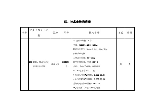
序号
设备(服务)名称
品牌
型号
技术参数
单位
数量
1
LED封装、测试与设计应用实训系统
武汉光驰
GCLEDFZ-B
1)金丝球焊机3台
电源:AC220V±10%(50Hz)
超声波时间5-200ms±5%(20ms/格)
多种弧形选择
压力调节范围:30-180g
温度控制范围:室温-400°C
成球:负电子成球,直径可调
选择功能:脚动、自动自由转换
7)离子风机10台
可提供平衡离子气流消除或中和宽范围集中目标或不易接触区域的静电荷。风量范围可连续调节,离子平衡度可达正、负十伏。
8)沾胶机(气动)1台
电源:AC220V±10%,50Hz,650VA
要求独立插座并可靠接地
常用气压:0.6兆帕
机械移动行程:XYZ方向300*300*100mm
注胶行程:10 mm,注胶速度5-6K/H
9)LED灌胶机1台
额定电压:220V,频率:50HZ,功率:50W,气缸:0-25mm
10)气动起模机1台
气压:1.5-2.5Kg。≥15升泵、额定电压/频率220V/50HZ
气压范围3-8kg/c㎡、气缸行程≥70mm
11)真空箱(15升泵)1台
额定电压:380V,频率:50HZ
量程:0.5N-10N
22)温度测试仪1个
测烤箱温度用
23)光色电综合测试系统1台
序号指标测试量程分辨率精度电参数
1正向电流30uA~5mA 0.01 mA 2uA±0.8%
5-500mA 0.01 mA 0.1mA±0.5%
50-3000mA 0.1mA 0.5mA±0.5%
LED_performance

热特性确定实际应用中 LED 的性能andras PoPPe, Mentor GraPhics corP.rePaPetih M e c h a n i c a l a n a l y s i s W介绍必须清楚地了解 LED 内部从 PN 结到环境的热特性,从而确保得到一个安全,可靠的设计和令人满意的性能。
在热流路径中可能有裸芯片或胶层等多个导热界面,并且它们的厚度和热阻很难在生产过程中进行控制。
此外,在 LED 封装和作为散热器的照明设备外壳之间的导热界面进一步增加了设计的挑战性。
必须在样机阶段尽可能早地了解 LED 的热阻值。
电流,颜色和效能LED 的光输出特性主要取决于其工作条件。
前向电流增加会使 LED 产生更多的光。
但当前向电流保持不变,光输出会随着 LED 的温度升高而下降。
图 1 描述了温度,电流和光输出的关系。
并且描述了一个 LED 相关的颜色光谱在峰值波长处的偏移。
用于普通照明的单色 LED,蓝色光谱的峰值会发生偏移,因此改变了 LED 所谓的色温。
这会对 LED 照明空间内的感官产生影响。
像很多其它产品一样,照明系统设计时也要权衡成本和性能。
功率分配及因此产生的散热需求很大程度上是由 LED 的能量转换效率所决定。
其定义为发出的光能和输入电功率的比值。
能效值与另一个度量参数效能有密切关系,它是一个关于有用性的评价指数,可感知的光除以提供的电功率的比值。
效能被用于评估不同光源的优劣。
不幸的是 LED 的效能会随着 LED 结温的增加而下降。
预测 LED 的输出光通量是照明设计的最终目标。
提供有效散热的热管理解决方案可以在 LED 实际应用中产生更多一致颜色的光通量。
热量从 LED 封装芯片开始传递,相关的数据由供应商提供。
图 2 中显示的是常见的导热结构。
一个 LED 灯大约50% 的结点至环境的热阻由 LED 封装所引起。
图1: 电流和温度依赖于一个LED 光输出中光谱强度分布图2: 功率 LED 的典型热传导结构传统的 LED 标准需要进一步地完善。
各种封装的Rth热阻参数Thermal-Design

FACTORS AFFECTING Rth(j-a)
There are several factors which affect the characteristic thermal resistance of IC packages. Some of the more significant of these include the test board configuration, the lead frame material, the design of the lead frame and the moulding compound.
Rth(j-a) = Rth(j-c) + Rth(c-a)
Rth(j-c) is the impedance from junction to case (outside surface of package) and Rth(c-a) is the impedance from case to ambient. It is sometimes useful to use only the Rth(c-a) to describe high performance packages where case temperatures are important and externally attached heat radiators may need to be attached. In these cases the overall Rth(j-a) will also include the contribution of the heat radiator.
- 1、下载文档前请自行甄别文档内容的完整性,平台不提供额外的编辑、内容补充、找答案等附加服务。
- 2、"仅部分预览"的文档,不可在线预览部分如存在完整性等问题,可反馈申请退款(可完整预览的文档不适用该条件!)。
- 3、如文档侵犯您的权益,请联系客服反馈,我们会尽快为您处理(人工客服工作时间:9:00-18:30)。
EIA/JEDEC Standard No. 51-1 INTEGRATED CIRCUIT THERMAL MEASUREMENT METHOD - ELECTRICAL TEST METHOD (SINGLE SEMICONDUCTOR DEVICE) Contents
page
1. INTRODUCTION
3
4 4 5 6 7 8 10 11
3. MEASUREMENT PROCEDURE
3.1 DEVICE CONNECTION 3.1.1 THERMAL TEST DIE 3.1.2 ACTIVE DIE 3.2 MEASUREMENT CURRENT DETERMINATION 3.3 K FACTOR CALIBRATION 3.4 TEST CONDITION DETERMINATION 3.4.1 HEATING CONDITIONS 3.4.2 MEASUREMENT CONDITIONS 3.5 TEST CONDITION CORRECTION 3.6 THERMAL STEADY-STATE DETERMINATION 3.7 DATA VALIDITY 3.8 TEST CONDITION SUMMARY
1 PURPOSE 1.2 SCOPE 1.3 RATIONALE 1.4 REFERENCES 1.5 DEFINITIONS
1
1 1 1 2 2
2. MEASUREMENT BASICS
2.1 TEMPERATURE-SENSITIVE PARAMETER 2.1.1 MEASUREMENT CURRENT CONSIDERATIONS 2.1.2 K FACTOR CALIBRATION 2.2 COOLING TIME CONSIDERATIONS 2.3 HEATING TIME CONSIDERATIONS 2.4 TEST WAVEFORMS 2.5 ENVIRONMENTAL CONSIDERATIONS 2.6 TEST SETUP
ENGINEERING DEPARTMENT
NOTICE JEDEC standards and publications contain material that has been prepared, reviewed, and approved through the JEDEC Council level and subsequently reviewed and approved by the EIA General Counsel. JEDEC standards and publications are designed to serve the public interest through eliminating misunderstandings between manufacturers and purchasers, facilitating interchangeability and improvement of products, and assisting the purchaser in selecting and obtaining with minimum delay the proper product for use by those other than JEDEC members, whether the standard is to be used either domestically or internationally. JEDEC standards and publications are adopted without regard to whether or not their adoption may involve patents or articles, materials, or processes. By such action JEDEC does not assume any liability to any patent owner, nor does it assume any obligation whatever to parties adopting the JEDEC standards or publications. The information included in JEDEC standards and publications represents a sound approach to product specification and application, principally from the solid state device manufacturer viewpoint. Within the JEDEC organization there are procedures whereby a JEDEC standard or publication may be further processed and ultimately become an EIA standard. No claims to be in conformance with this standard may be made unless all requirements stated in the standard are met. Inquiries, comments, and suggestions relative to the content of this JEDEC standard or publication should be addressed to JEDEC Solid State Technology Division, 2500 Wilson Boulevard, Arlington, VA 22201-3834, (703)907-7560/7559 or \jedec. Published by ©ELECTRONIC INDUSTRIES ALLIANCE Engineering Department 2500 Wilson Boulevard Arlington, VA 22201-3834 "Copyright" does not apply to JEDEC member companies as they are free to duplicate this document in accordance with the latest revision of JEDEC Publication 21 "Manual of Organization and Procedure". PRICE: Please refer to the current Catalog of JEDEC Engineering Standards and Publications or call Global Engineering Documents, USA and Canada (1-800-854-7179), International (303-397-7956) Printed in the U.S.A. All rights reserved
-ii-
EIA/JEDEC Standard No. 51-1 Page 1 1. INTRODUCTION 1.1 PURPOSE The purpose of this test method is to define a standard Electrical Test Method (ETM) that can be used to determine the thermal characteristics of single integrated circuit devices housed in some form of electronic package. This method will provide a basis for comparison of different devices housed in the same electronic package or similar devices housed in different electronic packages. By virtue of the standardizing of all pertinent terms, this method also improves the communication and exchange of information relative to the thermal characteristics of electronic packages housing a single semiconductor device. 1.2 SCOPE The measurement method described herein is equally applicable to both thermal test die and active integrated circuit devices. Thermal test die, consisting of a heat source and temperature sensor integrated into a semiconductor chip, are commonly used for package thermal characterization efforts, especially when one package is being compared to another. Integrated circuit devices, operating in an active mode that approximates intended applications, are used when specific application-oriented specification information is required. The measurement is limited to a single die (either test die or active die) housed in a package intended for a single die. 1.3 RATIONALE Increased requirements for semiconductor performance, reliability, quality, and lower cost have forced the need for knowledge of the semiconductor device junction temperature. However, without a well-defined standard methodology for making thermal measurements, it has become increasingly difficult to accurately determine junction temperature under actual operating and environmental conditions. Knowing the semiconductor device thermal resistance for a specific electronic package allows both the manufacturer and user to determine the junction temperature of the device. Accurate and correct thermal measurements are difficult to make because of the many variables that impact the final results. Electrical considerations (such as power, voltage and current levels, input and output levels, etc.), environmental considerations (mounting configuration, surroundings, mounting methodology, etc.) and selection of the junction temperature sensor will directly affect the thermal measurement. It should also be noted that the thermal characteristics of any semiconductor device are not necessarily constant with temperature or power dissipation, thus requiring thermal measurements under conditions that approximate actual operation in the applications.