P521pdfdatasheet-芯片资料介绍
2N5551中文资料(fairchild)中文数据手册「EasyDatasheet - 矽搜」
50 VCB = 100V
10
10
10
1β
100 Co
o
125 C
0.1
o
-40 Co
25 Co
75 C
- CCEO(SALT)LECTOR-EMITTER VOLTAGE [V]
0.01
V
1
10
100
IC- COLLECTOR CURRENT [mA]
Figure 2. Collector-Emitter Saturation Voltage vs.
芯片中文手册,看全文,戳
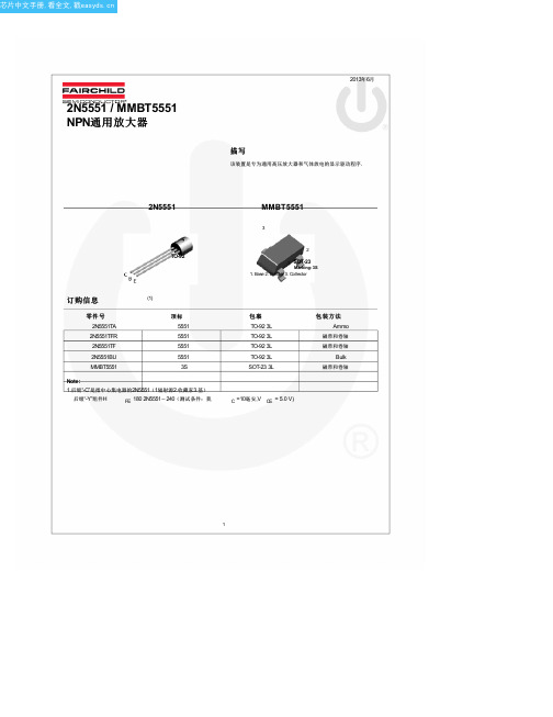
2N5551 / MMBT5551 NPN通用放大器
2013年6月
描写
该装置是专为通用高压放大器和气体放电的显示驱动程序.
2N5551
TO-92
MMBT5551
3
2
1 SOT-23
Marking: 3S 1. Base 2. Emitter 3. Collector
MMBT5551
350 2.8
357
Units
mW mW/°C °C/W °C/W
2
芯片中文手册,看全文,戳
电气特性
(4)
价值观是在T 符
A = 25°C除非另有说明. 参数
断特性
V(BR)CEO 集电极 - 发射极击穿电压 V(BR)CBO 集电极基击穿电压 V (BR)EBO 发射极基极击穿电压
Value
160 180
6 600 -55到+150
2N5551 / MMBT5551 - NPN通用放大
器
Units
V V V mA °C
热特性
价值观是在T
LED显示屏单元板常用芯片参数说明方便客户维修维护【LED显示屏维修资料】

上海元国光电科技常用器件的介绍随着LED显示屏工程商越来越多,生意越做越火爆,显示屏的问题也水涨船高,通常最头疼的问题就是显示屏的主要组成部分:单元板,新手一般不知道LED单元板维修时从哪里下手,围绕这个问题,我们总结了一下常见的问题及排除,提起74HC595,我想大家都不陌生,595也就是单元板的模块或者灯珠的垂直驱动芯片,一般单元板出现垂直一组灯不亮或者常亮,基本上都是这个芯片出现了问题或者虚焊,我们再来介绍下4953,它的作用是模块或者灯珠的行驱动,当LED单元板出现水平一条或者两条灯不亮的现象,也就是4953这个芯片的问题,至于其它芯片的作用及介绍,如下所述:1.IC的管脚功能IC芯片分别:74HC245、74HC595、74HC138、74HC04、4953。
各IC管脚功能如下:A: 74HC245功能是放大及缓冲。
各引脚如图120 和1接电源(+5V)19脚和10脚接电源地(GND)当电源是以上接时:输入脚分别为2、3、4、5、6、7、8、9。
输出脚分别为11、12、13、14、15、16、17、18注:2脚输入时,18脚输出。
其它脚以此类推。
B:74HC138功能是8选1译码器,输出为8行。
控制行数据。
各引脚如图2第8脚GND,电源地。
第16脚VCC,电源正极第1-3脚A、B、C输入脚。
第4-6脚选通输入端,(一般第5脚为EN )9-15脚和第7脚输出端。
C:74HC595功能是8位串入、并出移位寄存器。
控制列数据。
各引脚如图316脚和10脚接电源(+5V),13脚和8脚接电源地(GND)。
列信号输出脚:1、2、3、4、5、6、7、15。
第一列输出脚为7脚,以此类推。
另第八列输出脚为15脚。
数据信号输入脚(Din)为14,数据信号输出脚(Din)为9。
锁存信号脚(L)为12脚,移位信号脚为11脚。
D:74HC04功能是六带缓冲反相器,控制使零信号(EN)。
各引脚如下图15脚接电源(+5V),7脚电源地(GND)。
启英泰伦 CI2311 数据手册说明书

CI2311数据手册高性能神经网络智能语音芯片TSSOP24长7.8mm 宽6.4mm 高1.2mm•脑神经网络处理器(BNPU)–BNPU V3,支持DNN\TDNN\RNN\CNN 等神经网络及并行矢量运算,可实现语音识别、声纹识别、命令词自学习、语音检测及深度学习降噪等功能•CPU 和存储器–CPU 主频可达240MHz –内置1MBytes Flash 存储器–内置640KBytes SRAM–内置512bit eFuse,可用于应用加密•Audio Codec–高性能低功耗audio ADC,SNR ≥95dB –低功耗audio DAC,SNR ≥95dB •音频接口–1路双通道PDM 接口•ADC 和PWM–内置2通道12bit SAR ADC –支持3路PWM 接口•GPIO–7个高速GPIO,响应速率可达20MHz –其中5个GPIO 支持5V 输入•复位和电源管理–内置电源管理单元PMU–PMU 输入电压范围:3.6V 到5.5V –内置上电复位(POR)–内置电压检测(PVD)•时钟–16MHz 外接晶体振荡器•通讯接口–1路IIC 接口–2路UART 接口,支持5V 通讯,支持最高3Mbps 速率•定时器和看门狗–内置4组32位定时器和2组看门狗•无线–GFSK 调制方式,1Mbps 模式的接收灵敏度可达-90dBm–最大发射输出功率达+8dBm –支持BLE 广播–频道切换快,可以实现多频道调频算法目录1概述 (3)1.1功能描述 (3)1.2芯片规格 (4)2引脚图和功能描述 (7)2.1引脚图 (7)2.2管脚描述 (8)2.3复用功能 (10)3电气特性 (11)4无线特性 (12)5封装信息 (13)6订购信息 (14)7应用方案 (15)7.1应用参考电路图 (15)7.2应用其它注意事项 (16)1概述1.1功能描述CI2311是启英泰伦研发的新一代高性能神经网络智能语音芯片,集成了启英泰伦自研的脑神经网络处理器BNPU V3和CPU内核,系统主频可达240MHz,内置高达640KByte的SRAM,集成PMU电源管理单元,集成双通道高性能低功耗Audio Codec和多路UART、IIC、PWM、GPIO、PDM等外围控制接口,集成2.400~2.483GHz世界通用ISM频段无线收发芯片,嵌入了基带通讯协议。
74F00D_PHILIPS_74121-芯片资料介绍

DIP14:plastic dual in-line package; 14 leads (300 mil)SOT27-1SO14:plastic small outline package; 14 leads; body width 3.9 mm SOT108-1NOTESDefinitionsShort-form specification — The data in a short-form specification is extracted from a full data sheet with the same type number and title. For detailed information see the relevant data sheet or data handbook.Limiting values definition — Limiting values given are in accordance with the Absolute Maximum Rating System (IEC 134). Stress above one or more of the limiting values may cause permanent damage to the device. These are stress ratings only and operation of the device at these or at any other conditions above those given in the Characteristics sections of the specification is not implied. Exposure to limiting values for extended periods may affect device reliability.Application information — Applications that are described herein for any of these products are for illustrative purposes only. Philips Semiconductors make no representation or warranty that such applications will be suitable for the specified use without further testing or modification.DisclaimersLife support — These products are not designed for use in life support appliances, devices or systems where malfunction of these products can reasonably be expected to result in personal injury. Philips Semiconductors customers using or selling these products for use in such applications do so at their own risk and agree to fully indemnify Philips Semiconductors for any damages resulting from such application.Right to make changes — Philips Semiconductors reserves the right to make changes, without notice, in the products, including circuits, standard cells, and/or software, described or contained herein in order to improve design and/or performance. Philips Semiconductors assumes no responsibility or liability for the use of any of these products, conveys no license or title under any patent, copyright, or mask work right to these products, and makes no representations or warranties that these products are free from patent, copyright, or mask work right infringement, unless otherwise specified.Philips Semiconductors811 East Arques AvenueP.O. Box 3409Sunnyvale, California 94088–3409Telephone 800-234-7381© Copyright Philips Electronics North America Corporation 1998All rights reserved. Printed in U.S.A.print code Date of release: 10-98。
P521-48中文资料

PreliminaryP521-48Low Phase Noise PECL VCXO (27MHz to 65MHz)FEATURES• 27MHz to 65MHz Fundamental Mode Crystal. • Output range: 27MHz – 65MHz. • Complementary PECL outputs.• Selectable OE Logic (enable high or enable low). • Integrated variable capacitors. • High pull linearity: < 5%. • +/- 125 ppm pull range• Supports 2.5V or 3.3V-Power Supply. • Available in die form. • Thickness 10 mil.DESCRIPTIONSP521-48 is a VCXO IC specifically designed to pull high frequency fundamental crystals. Its internal varicaps allow an on chip frequency pulling,controlled by the VCON input. The chip provides a low phase noise, low jitter PECL differential clock output.BLOCK DIAGRAMDIE CONFIGURATIONDIE SPECIFICATIONSName Value Size 56.5 x 57.5 milReverse side GND Pad dimensions 80 micron x 80 micronThickness10 milOUTPUT ENABLE LOGIC SELECTIONOESEL (Pad #14) OECTRL (Pad #22) State0 (Default)Output enabled 0 (Default)1 Tri-state 0 Tri-state11 (Default)Output enabledPad #14, 22: Bond to GND to set to “0”, bond to VDD to set to “1”No connection results to “default” setting through internal pull-up/-down. Pad #22: Logical states defined by PECL V I H and V I L levels.YX(0,0)(1460,1435)Preliminary P521-48Low Phase Noise PECL VCXO (27MHz to 65MHz) PAD ASSIGNMENT AND DESCRIPTIONPad # Name X (µm) Y (µm) Description1 VCON 329.6 110.1 Control Voltage input. Use this pin to change the output frequency by varying the applied Control Voltage.2 GNDOSC 498.3 110.0 GND connection for oscillator circuitry.3 GNDANA 696.2 110.0 GND connection for analog circuitry.4 GNDANA 825.0 110.0 GND connection for analog circuitry.5 GNDBUF 973.6 110.0 GND connection for output buffer circuitry.6 GNDBUF 1150.0 109.1 GND connection for output buffer circuitry.7 GNDBUF (optional) 1183.6 302.2 GND connection for output buffer circuitry.8 PECL 1183.6 452.3 PECL output9 PECLBAR 1183.6 613.5 PECL complementary output.10 VDDBUF (optional) 1182.4 745.9 VDD connection for output buffer circuitry. VDDBUF should be separately decoupled from other VDDs whenever possible.11 VDDBUF 1252.4 903.6 VDD connection for output buffer circuitry. VDDBUF should be separately decoupled from other VDDs whenever possible.12 VDDANA 1252.4 1081.3 VDD connection for analog circuitry.VDDANA should be separately decoupled from other VDDs whenever possible.13 Not used 1058.5 1221.614 OESEL 864.5 1221.6 Selector input to choose the OE control logic. See table on page 1.15 VDDOSC 624.0 1222.7 VDD connection for oscillator circuitry.VDDOSC should be separately decoupled from other VDDs whenever possible.16 Not used 467.1 1222.617 OSCOFF 271.1 1222.6 Oscillator Off Selection input pad. When low, turns off the oscillator when output is disabled. When high (default), oscillator running when output is disabled. Internal pull-up18 GNDOSC (optional) 109.4 1222.9 GND connection for oscillator circuitry.19 VCON 108.9 1062.1 Control Voltage input. Use this pin to change the output frequency by varying the applied Control Voltage (internally connected to pad 1).20 XIN 109.0 865.8 Crystal oscillator input pad.21 XOUT 108.6 358.4 Crystal oscillator output pad.22 OECTRL 108.6 146.5 OE input pad. See table on page 1. Note: for optimal Phase Noise performance, it is recommended to bond all optional VDD and GND pads.Preliminary P521-48Low Phase Noise PECL VCXO (27MHz to 65MHz) ELECTRICAL SPECIFICATIONS1. Absolute Maximum RatingsPARAMETERS SYMBOL MIN. MAX. UNITS Supply Voltage V DD7 VInput Voltage, dc V I V SS-0.5 V DD+0.5 V Output Voltage, dc V O V SS-0.5 V DD+0.5 V Storage Temperature T S-65 150 °C Ambient Operating Temperature T A0 70 °C Junction Temperature T J125 °CLead Temperature (soldering, 10s) 260 °CInput Static Discharge Voltage Protection 2 kV Exposure of the device under conditions beyond the limits specified by Maximum Ratings for extended periods may cause permanent damage to the device and affect product reliability. These conditions represent a stress rating only, and functional operations of the device at these or any other conditions above the operational limits noted in this specification is not implied.2. Crystal SpecificationsPARAMETERS SYMBOL CONDITIONS MIN. TYP. MAX. UNITS Crystal Resonator Frequency F XIN Parallel Fundamental Mode 27 65 MHz Crystal Loading Rating C L (xtal)Die at VCON = 1.65V 7.5 pF Interelectrode Capacitance C0 3.5 pF Crystal Pullability C0/C1 (xtal)AT cut 250 - Recommended ESR R E AT cut 30 Ω3. Voltage Control Crystal OscillatorPARAMETERS SYMBOL CONDITIONS MIN. TYP. MAX. UNITS VCXO Stabilization Time * T VCXOSTB From power valid 10 ms VCXO Tuning Range XTAL C0/C1 < 250 250* ppmCLK output pullability 0V ≤ VCON ≤ 3.3Vat room temperature±80* ppmOn-chip Varicaps control range VCON = 0 to 3.3V 4 – 18* pF Linearity 4* 5* % VCXO Tuning Characteristic 65 ppm/V VCON input impedance 2000 kΩVCON modulation BW 0V ≤ VCON ≤ 3.3V, -3dB 25 kHz Note: Parameters denoted with an asterisk (*) represent nominal characterization data and are not production tested to any specific limits.PreliminaryP521-48Low Phase Noise PECL VCXO (27MHz to 65MHz)4. General Electrical SpecificationsPARAMETERSSYMBOLCONDITIONSMIN.TYP.MAX.UNITSSupply Current (Loaded Outputs) I DD at 3.3V @ 61.44MHz 45 mA Oscillator off 10 Output valid after OE enabled Oscillator on 1 ms Operating Voltage V DD2.253.63 V Output Clock Duty Cycle @ Vdd – 1.3V (PECL) 45 50 55 % Short Circuit Current±50mA5. Jitter specificationsPARAMETERSCONDITIONSMIN.TYP.MAX.UNITSPeriod jitter RMS at 61.44MHz 2.5 Period jitter peak-to-peak at 61.44MHz At 61.44MHz, with capacitivedecoupling between VDD and GND. Over 10,000 cycles18.5 20 psAccumulated jitter RMS at 61.44MHz2.5 Accumulated jitter peak-to-peak at 61.44MHz At 61.44MHz, with capacitivedecoupling between VDD and GND.Over 1,000,000 cycles. 24 27 ps Random Jitter“RJ” measured on Wavecrest SIA 3000 2.5 ps Integrated jitter RMS at 61.44MHzIntegrated 12 kHz to 20 MHz0.60.75psMeasured on Wavecrest SIA 30006. Phase noise specifications PARAMETERS FREQUENCY10Hz100Hz1kHz10kHz100kHz1MHzUNITSPhase Noiserelative to carrier61.44MHz-75-100-125-140-145-150dBc/HzNote: Phase Noise measured at VCON = 0VPreliminaryP521-48Low Phase Noise PECL VCXO (27MHz to 65MHz)7. PECL Electrical CharacteristicsPARAMETERSSYMBOLCONDITIONSMIN.MAX.UNITSOutput High Voltage V OH V DD – 1.025V Output Low VoltageV OLR L = 50 Ω to (V DD – 2V)(see figure)V DD – 1.620V8. PECL Switching CharacteristicsPARAMETERSSYMBOLCONDITIONSMIN.TYP.MAX.UNITSClock Rise Time t r @20/80% - PECL 0.6 1.5 ns Clock Fall Timet f@80/20% - PECL0.51.5nsOUTOUTPECL Levels Test CircuitPECL Transistion Time WaveformOUTOUT50%OUTOUTt SKEWPECL Output Skew2.0VPreliminary P521-48Low Phase Noise PECL VCXO (27MHz to 65MHz) ORDERING INFORMATIONPhaseLink Corporation, reserves the right to make changes in its products or specifications, or both at any time without notice. The information furnished by Phaselink is believed to be accurate and reliable. However, PhaseLink makes no guarantee or warranty concerning the accuracy of said information and shall not be responsible for any loss or damage of whatever nature resulting from the use of, or reliance upon this product.LIFE SUPPORT POLICY: PhaseLink’s products are not authorized for use as critical components in life support devices or systems without theexpress written approval of the President of PhaseLink Corporation.。
MiCOM P521 技术说明书(v1.B)

¢¡
£¥¤§¦©¨¢
$ $0 22
/
$
! "#$&%('
$
$
ÔÖÕØ× ÙÛ ÔÚ ÜàÝ ß
$,
ÙÛ ÔÚ ÜÞÝß
%
%
Ù ÔØ×
$,
$. 1,
/
$
$
#0
Ó + þÄÍm¨§ PX¨»£(H§Ïá5H¿XAXB}X~¢5£(H$R|XS¡´X w5Ó¥m5¨»£(H§Û5id§GXåXq|)â X£RHÔ`ã¢|¥ä¥åxGÓ ·¥G7gx§æ¥çT idG£RHÔ vE¢|GÓ æ¥¢EF¢ &¢Í`IÄ&¥m¨G£RHè7é7êF7&Þ(XexÔÍ¡ ë7ì7í&`7&Ó (¨¥w§î gXÃTx¥ïXf ð¢¢dG£If§ñT¨¥w¥ò7ä& ÚP¨G£RH¢xGÓ $, Àm¨&£RHTvX $, Rvm¨©¢exGÓ·7g¢v¥©TÛ ýGþR7ó¢¬ÿ¢F % eÎIA¥É7ͧeÛº5aubÈÔX£@£W5YA¥É¥ô7õ&¥&Ó m¨G£RHÂÄÃxÔÍ(m¨G£RHX¢7·7gx&T£ö % ¿¥ÌÄGÓ $, em¨7©ÃTxÔÍ(ÄXTÛ¥÷ºÔ@Ê@ËW5YË57&Ó % sGoø¥ùÎ s¥ú ïÈEf û ÅX 3$. 1,34$, Í û
YTxq¢| FG£RH Þ`5£RH aF¢tw£RH m¨G£RH¢yP¨G£RH åG£RH wuxSz¨{T|x }~Ý¢
+
ò
! "#$&%('
S
(#
bEc§d1e)f gq¢rst h¢W5Yst huXu ¢¨¢st
P521光电耦合器

P521光电耦合器P521 光电耦合器最佳答案:摘要线性光耦合器是目前国际上正推广应用的一种新型光电隔离器件。
文中介绍其性能特点、产品分类,以及它在单片开关电源中的应用。
关键词光耦合器线性电流传输比通信单片开关电源光耦合器(optical coupler,英文缩写为OC)亦称光电隔离器或光电耦合器,简称光耦。
它是以光为媒介来传输电信号的器件,通常把发光器(红外线发光二极管LED)与受光器(光敏半导体管)封装在同一管壳内。
当输入端加电信号时发光器发出光线,受光器接受光线之后就产生光电流,从输出端流出,从而实现了“电—光—电”转换。
普通光耦合器只能传输数字(开关)信号,不适合传输模拟信号。
近年来问世的线性光耦合器能够传输连续变化的模拟电压或模拟电流信号,使其应用领域大为拓宽。
1 光耦合器的类型及性能特点1.1 光耦合器的类型光耦合器有双列直插式、管式、光导纤维式等多种封装形式,其种类达数十种。
光耦合器的分类及内部电路如图1所示。
图中是8种典型产品的型号:(a)通用型(无基极引线);(b)通用型(有基极引线);(c)达林顿型;(d)高速型;(e)光集成电路;(f)光纤型;(g)光敏晶闸管型;(h)光敏场效应管型。
1.2 光耦合器的性能特点光耦合器的主要优点是单向传输信号,输入端与输出端完全实现了电气隔离,抗干扰能力强,使用寿命长,传输效率高。
它广泛用于电平转换、信号隔离、级间隔离、开关电路、远距离信号传输、脉冲放大、固态继电器(SSR)、仪器仪表、通信设备及微机接口中。
在单片开关电源中,利用线性光耦合器可构成光耦反馈电路,通过调节控制端电流来改变占空比,达到精密稳压目的。
光耦合器的技术参数主要有发光二极管正向压降VF、正向电流IF、电流传输比CTR、输入级与输出级之间的绝缘电阻、集电极-发射极反向击穿电压V(BR)CEO、集电极-发射极饱和压降VCE(sat)。
此外,在传输数字信号时还需考虑上升时间、下降时间、延迟时间和存储时间等参数。
ECA1HM221中文资料(panasonic)中文数据手册「EasyDatasheet - 矽搜」
10000 16
31.5 1600 0.42 0.8 7.5
ECA1AM103
15000 18
35.5 1850 0.52 0.8 7.5
ECA1AM153
10 5
11
30 0.20 0.5 2.0 5.0 2.5 ECA1CM100( )
22 5
11
75 0.20 0.5 2.0 5.0 2.5 ECA1CM220( )
引线空间
直行
编带编带
½B ½i
型号
最小包装台数
直行
大坪
Leads
(V) (µF) (毫米) (毫米)(毫安均方根) (毫米) (毫米) (毫米) (毫米)
(pcs) (pcs)
220 5
11
240 0.28 0.5 2.0 5.0 2.5 ECA0JM221( )
200 2000
470 6.3 11.2 380 0.28 0.5 2.5 5.0 2.5 ECA0JM471( )
– EEE-112 –
00 Nov. 2012
芯片中文手册,看全文,戳
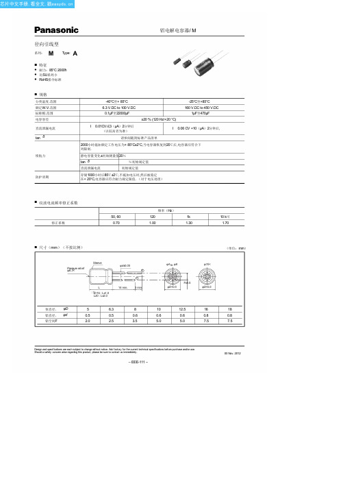
铝电解电容器/ M
■ 标准产品
耐力:85°C 2000ħ
机箱尺寸
规范
引线长度
W.V.
Cap. (±20 %)
Dia.
长度
纹波晒黑 δ 铅
当前
Dia.
(120赫兹)(120赫兹)
(+85 °C) (+20 °C)
ECA1VM471( )
200 500
1000 12.5 20
900 0.14 0.6 5.0 5.0
35
2200 16
25 1250 0.16 0.8 7.5 7.5