LT1081中文资料
ZXCT1081E5TA;中文规格书,Datasheet资料

ZXCT1081HIGH VOLTAGE HIGH-SIDE CURRENT MONITORDescriptionThe ZXCT1081 is a high side current sense monitor with a gain of 10 and a voltage output. Using this device eliminates the need to disrupt the ground plane when sensing a load current.The wide input voltage range of 40V down to as low as 3V make it suitable for a range of applications; including systems operating from industrial 24-28V rails and power supplies.Pin AssignmentsFeatures• 3V to 40V continuous high side voltage • Accurate high-side current sensing • Output voltage scaling x10 •4.5V to 12V V CC range• Low quiescent current:o 80 μA supply pino 30 μA I SENSE +• SOT23-5 package • -40°C to 125°C ambient temperature rangeApplications• Automotive current measurement• Industrial applications current measurement • Battery management • Over current monitor • Power management • Power adaptersTypical Application CircuitV SENSE-SENSE+V CC GND OUTZXCT1081Pin DescriptionPin Name Description1 VCC This is the analogue supply and provides power to internal circuitry2 GND Ground pin3 OUT Output voltage pin. NMOS source follower with 20μA bias to ground4 SENSE+ This is the positive input of the current monitor and has an input range from 40V(60V transient) down to 3V. The current through this pin varies with differential sensevoltage5 SENSE-This is the negative input of the current monitor and has an input range from 40V(60V transient) down to 3VAbsolute Maximum RatingsParameter Rating UnitContinuous Voltage on SENSE+ and SENSE- -0.6 and 45 V Transient Voltage on SENSE+ and SENSE- -0.6 and 65 V Voltage On All Other Pins -0.6 and 14 VDifferential Sense Voltage, V SENSE800 mV Operating Temperature -40 to 125 °C Storage Temperature -55 to 150 °C Maximum Junction Temperature 125 °CPackage Power Dissipation 300 @ T A = 25°C (de-rate to zero at 125°C)mWOperation above the absolute maximum rating may cause device failure. Operation at the absolute maximum ratings, for extended periods, may reducedevice reliabilityRecommended Operating ConditionsSymbol Parameter Min Max Units V IN Common-Mode Sense+ Input Range 3 40 V V CC Supply Voltage Range4.5 12 V V SENSE Differential Sense Input Voltage Range 0 0.15 V V OUT Output Voltage Range 0 1.5 V T JAmbient Temperature Range-40125°CElectrical Characteristics (Test conditions: T A = 25°C, V IN = 12V, V CC = 5V, V SENSE (a) = 100mV unless otherwise stated)Symbol Parameter ConditionMin.Typ. Max.UnitI CC VCC Supply Current V CC = 12V 40 80 120 µA I SENSE +SENSE+ Input Current 15 30 60 µA I SENSE -SENSE- Input Current 10 40 80 nAV O(0) Zero V SENSE (a) error (b) V SENSE (a)= 0V0 35 mV V O(10) Output Offset Voltage (c) V SENSE (a)= 10mV-30 +30 mV Gain ΔV OUT /ΔV SENSE (a) V SENSE (a)= 10mV to 150mV9.95 10 10.05 V OUT TC (d)V OUT Variation with Temperature30 ppm/°C A CCTotal Output Error -3 3 % I OH Output Source Current V OUT = 30mV 1 mA I OL Output Sink Current V OUT = +30mV20 µA PSRR VCC Supply Rejection Ration V CC = 4.5V to 12V 54 60 dB CMRR Common-Mode Sense Rejection Ratio V IN + 40V to 3V 60 75 dBBW -3dB Small Signal Bandwidth V SENSE (a)(AC) = 10mV pp50 kHz Notes:(a) VSENSE = "V SENSE +" - "V SENSE -"(b) The ZXCT1081 operates from a positive power rail and the internal voltage-current converter current flow is unidirectional; these result in the output offset voltage for V SENSE = 0V always being positive.(c) For V SENSE > 10mV, the internal voltage-current converter is fully linear. This enables a true offset to be defined and used. V O(10) is expressed as the variance about an output voltage of 100mV>.(d)Temperature dependent measurements are extracted from characterization and simulation results.Typical Operating Conditions (Cont.)Application InformationThe ZXCT1081 has been designed to allow it to operate with 5V supply rails while sensing common mode signals up to 40V. This makes it well suited to a wide range of industrial and power supply monitoring applications that require the interface to 5V systems while sensing much higher voltages.To allow this its VCC pin can be used independently of SENSE+.Figure 1 shows the basic configuration of the ZXCT1081.VFigure 1 Typical Configuration of ZXCT1081Load current from the input is drawn through R SENSE developing a voltage V SENSE across the inputs of the ZXCT1081.The internal amplifier forces V SENSE across internal resistance R SH causing a current to flow through MOSFET M1. This current is then converted to a voltage by R G . A ratio of 10:1 between R G and R SH creates the fixed gain of 10. The output is then buffered by the unity gain buffer.The gain equation of the ZXCT1081 is:V OUT = I L R SENSE x 1 = x R SENSE x 10The maximum recommended differential input voltage, V SENSE , is 150mV; it will however withstand voltages up to 800m Ω. This can be increased further by the inclusion of a resistor, R LIM , between SENSE- pin and the load; typical value is of the order of 10k .R G R SHFigure 2 Protection/Error Sources for ZXCT1081Capacitor CD provides high frequency transient decoupling when used with R LIM; typical values are of the order 10pF.For best performance R SENS E should be connected as close to the SENSE+ (and SENSE ) pins; minimizing any series resistance with R SENSE.When choosing appropriate values for R SENSE a compromise must be reached between in-line signal loss (including potential power dissipation effects) and small signal accuracy.Higher values for R SENSE gives better accuracy at low load currents by reducing the inaccuracies due to internal offsets. For best operation the ZXCT1081 has been designed to operate with V SENSE of the order of 50mV to 150mV.Current monitors' basic configuration is that of a unipolar voltage to current to voltage converter powered from a single supply rail. The internal amplifier at the heart of the current monitor may well have a bipolar offset voltage but the output cannot go negative; this results in current monitors saturating at very low sense voltages.As a result of this phenomenon the ZXCT1081 has been specified to operate in a linear manner over a V SENSE range of 10mV to 150mV range, however it will still be monotonic down to V SENSE of 0V.It is for this very reason that Zetex has specified an input offset voltage (V O(10)) at 10mV. The output voltage for any V SENSE voltage from 10mV to 150mV can be calculated as follows:V OUT = (V SENSE) xG + V O(10)Alternatively the load current can be expressed as:I L = V OUT – V O(10) GxR SENSEPackage Outline – SOT23-5DIMMillimeters Inches Min Max Min MaxA 0.90 1.45 0.03540.0570A1 0.00 0.15 0.00 0.0059 A2 0.90 1.3 0.0354 0.0511b 0.20 0.50 0.00780.0196C 0.09 0.26 0.00350.0102D 2.70 3.10 0.10620.1220E 2.20 3.20 0.08660.1181E1 1.30 1.80 0.0511 0.0708e 0.95REF 0.0374REF e1 1.90REF 0.0748REF L 0.10 0.60 0.00390.0236a° 0 30 0 30 Note: Controlling dimensions are in millimeters. Approximate dimensions are provided in inches分销商库存信息: DIODESZXCT1081E5TA。
LT6107中文资料
TEMPERATURE RANGE –55°C to 150°C
TEMPERATURE RANGE –55°C to 150°C
ELECTRICAL CHARACTERISTICS The ● denotes the specifications which apply over the full specified
0
VSENSE = 500mV, RIN = 500Ω, ROUT = 10k, V+ = 36V ● –0.45 –0.14
0.1
VOUT(HIGH)
Output Swing High (Referred to V+)
VSENSE = 120mV
1.2
●
1.4
μV μV μV/°C
nA nA nA
VSENSE = 5mV V+ = 12V, 36V
●
1
40
●
130
IOS
Input Offset Current
V+ = 12V, 36V
1
IOUT PSRR
Maximum Output Current Power Supply Rejection Ratio
(Note 3) V+ = 2.7V to 36V, VSENSE = 5mV
SYMBOL
BW tr IS
PARAMETER
CONDITIONS
MIN
Байду номын сангаас
Minimum Output Voltage (Note 5)
VSENSE = 0mV, RIN = 100Ω, ROUT = 10k ●
VSENSE = 0mV, RIN = 500Ω, ROUT = 10k, V+ = 12V, 36V ●
NCP1081资料

NCP1081Integrated High PowerPoE-PD Interface & DC-DC Converter ControllerIntroductionThe NCP1081 is a member of ON Semiconductor’s high power HIPO t Power over Ethernet Powered Device (PoE−PD) product family and represents a robust, flexible and highly integrated solution targeting demanding medium and high power Ethernet applications. It combines in a single unit an enhanced PoE−PD interface supporting the IEEE802.3af and the upcoming draft IEEE802.3at (D3.0) standard and a flexible and configurable DC−DC converter controller.The NCP1081’s exceptional capabilities offer new opportunities for the design of products powered directly over Ethernet lines, eliminating the need for local power adaptors or power supplies and drastically reducing the overall installation and maintenance cost. ON Semiconductor’s unique manufacturing process and design enhancements allow the NCP1081 to deliver up to 25.5 W for the draft IEEE802.3at (D3.0) standard and up to 40 W for proprietary high power PoE applications. The NCP1081 enables the draft IEEE802.3at (D3.0) and implements a two event physical layer classification. Additional proprietary classification procedures support high power power sourcing equipment (PSE) on the market. The unique high power features leverage the significant cost advantages of PoE−enabled systems to a much broader spectrum of products in emerging markets such as industrial ethernet devices, PTZ and Dome IP cameras, RFID readers, MIMO WLAN access points, high end V oIP phones, notebooks, etc.The integrated current mode DC−DC controller facilitates isolated and non−isolated fly−back, forward and buck converter topologies. It has all the features necessary for a flexible, robust and highly efficient design including programmable switching frequency, duty cycle up to 80 percent, slope compensation, and soft start−up.The NCP1081 is fabricated in a robust high voltageprocess and integrates a rugged vertical N−channel DMOS with a low loss current sense technique suitable for the most demanding environments and capable of withstanding harsh environments such as hot swap and cable ESD events. The NCP1081 complements ON Semiconductor’s ASSP portfolio in industrial devices and can be combined with stepper motor drivers, CAN bus drivers and other high−voltage interfacing devices to offer complete solutions to the industrial and security market.Powered Device Interface•Supporting the IEEE802.3af and the upcoming draft IEEE802.3at (D3.0) standard•Supports draft IEEE802.3at (D3.0) Two Event Layer 1 classification•High power Layer 1 classification indicator •Extended power ranges up to 40 W •Programmable classification current •Adjustable under voltage lock out •Programmable inrush current limit •Programmable operational current limit up to 1100mA for extended power ranges•Over−temperature protection•Industrial temperature range −40°C to 85°C with full operation up to 150°C junction temperature•0.6 ohm hot−swap pass−switch with low loss current sense technique•Vertical N−channel DMOS pass−switch offers the robustness of discrete MOSFETs with integrated temperature controlTSSOP−20 EPDE SUFFIXCASE 948ABSee detailed ordering and shipping information in the packagedimensions section on page 2 of this data sheet.ORDERING INFORMATIONNCP1081 = Specific Device CodeXXXX= Date CodeY= Assembly LocationZZ= Traceability CodeDC −DC Converter Controller•Current mode control•Supports isolated and non −isolated DC −DC converter applications•Internal voltage regulators•Wide duty cycle range with internal slope compensation circuitry•Programmable oscillator frequency •Programmable soft −start time(Top View)PIN DIAGRAMExposed Pad1SS FB COMP VDDL VDDH GATE ARTNnCLASS_AT CS OSCVPORTP CLASS UVLO INRUSH ILIM1VPORTN1RTN VPORTN2TEST1TEST2Ordering InformationPart NumberPackage Shipping Configuration †Temperature Range NCP1081DEG TSSOP −20 EP (Pb −Free)74 units / Tube −40°C to 85°C NCP1081DER2GTSSOP −20 EP (Pb −Free)2500 / Tape & Reel−40°C to 85°C†For information on tape and reel specifications, including part orientation and tape sizes, please refer to our Tape and Reel Packaging Specification Brochure, BRD8011/D.VPORTN1,2VPORTPCLASS INRUSH ILIM1VDDHnCLASS_AT VDDLRTNARTNSSFB COMP CSGATEOSCFigure 1. NCP1081 Block DiagramFigure 2. Isolated Fly−back ConverterFigure 2 shows the integrated PoE−PD switch and DC−DC controller configured to work in a fully isolated application. The output voltage regulation is accomplished with an external opto−coupler and a shunt regulator (Z1).Figure 3. Non−Isolated Fly−back ConverterFigure 3 shows the integrated PoE−PD and DC−DC controller configured in a non−isolated fly−back configuration. A compensation network is inserted between the FB and the COMP pin for overall stability of the feedback loop.Figure 4. Non−Isolated Fly−back with Extra WindingFigure 4 shows the same non−isolated fly−back configuration as Figure 3, but adds a 12V auxiliary bias winding on the transformer to provide power to the NCP1081 DC−DC controller via its VDDH pin. This topology shuts off the current flowing from VPORTP to VDDH and therefore reduces the internal power dissipation of the PD, resulting in higher overall power efficiency.Figure 5. Non−Isolated Forward ConverterFigure 5 shows the NCP1081 used in a non−isolated forward topology.High Power ConsiderationsThe NCP1081 is designed to implement various configurations of high−power PoE systems including those based on the developing IEEE 802.3at standard. High power operation can be enabled by a Dual Event Layer 1 classification or a Single Event Layer 1 classification combined with a Layer 2 high power classification. The NCP1081 also supports proprietary designs capable of delivering 25 W to 40 W to the load in two−pair configurations. A separate application note describes these implementations (“NCP1081 High Power PoE Applications”).Table 1. Pin DescriptionsName Pin No.Type DescriptionVPORTP1Supply Positive input power. Voltage with respect to VPORTN1,2.6,8Ground Negative input power. Connected to the source of the internal pass−switch.VPORTN1VPORTN2RTN7Ground DC−DC controller power return. Connected to the drain of the internal pass−switch. It mustbe connected to ARTN. This pin is also the drain of the internal pass−switch.ARTN14Ground DC−DC controller ground pin. Must be connected to RTN as a single point ground connectionfor improved noise immunity.VDDH16Supply Output of the 9V LDO internal regulator. Voltage with respect to ARTN. Supplies the internalgate driver. VDDH must be bypassed to ARTN with a 1m F or 2.2m F ceramic capacitor withlow ESR.VDDL17Supply Output of the 3.3V LDO internal regulator. Voltage with respect to ARTN. This pin can beused to bias an external low−power LED (1mA max.) connected to nCLASS_AT, and canalso be used to add extra biasing current in the external opto−coupler. VDDL must be by-passed to ARTN with a 330nF or 470nF ceramic capacitor with low ESR.CLASS2Input Classification current programming pin. Connect a resistor between CLASS and VPORTN1,2. INRUSH4Input Inrush current limit programming pin. Connect a resistor between INRUSH and VPORTN1,2. ILIM15Input Operational current limit programming pin. Connect a resistor between ILIM1 andVPORTN1,2.UVLO3Input DC−DC controller under−voltage lockout input. Voltage with respect to VPORTN1,2. Connecta resistor−divider from VPORTP to UVLO to VPORTN1,2 to set an external UVLO threshold. GATE15Output DC−DC controller gate driver output pin.OSC11Input Internal oscillator frequency programming pin. Connect a resistor between OSC and ARTN. nCLASS_AT13Output,Active−low, open−drain Layer 1 dual−finger classification indicator.Open DrainCOMP18I/O Output of the internal error amplifier of the DC−DC controller. COMP is pulled−up internally toVDDL with a 5 k W resistor. In isolated applications, COMP is connected to the collector of theopto−coupler. Voltage with respect to ARTN.FB19Input DC−DC controller inverting input of the internal error amplifier. In isolated applications, the pinshould be strapped to ARTN to disable the internal error amplifier.CS12Input Current−sense input for the DC−DC controller. Voltage with respect to ARTN.SS20Input Soft−start input for the DC−DC controller. A capacitor between SS and ARTN determines thesoft−start timing.TEST19Input Digital test pin must always be connected to VPORTN1,2.TEST210Input Digital test pin must always be connected to VPORTN1,2.EP Exposed pad. Connected to VPORTN1,2 ground.Table 2. Absolute Maximum RatingsSymbol Parameter Min.Max.Units Conditions VPORTP Input power supply−0.372V Voltage with respect to VPORTN1,2RTN ARTN Analog ground supply 2−0.372V Pass−switch in off−state(Voltage with respect to VPORTN1,2)VDDH Internal regulator output−0.317V Voltage with respect to ARTNVDDL Internal regulator output−0.3 3.6V Voltage with respect to ARTNCLASS Analog output−0.3 3.6V Voltage with respect to VPORTN1,2INRUSH Analog output−0.3 3.6V Voltage with respect to VPORTN1,2ILIM1Analog output−0.3 3.6V Voltage with respect to VPORTN1,2UVLO Analog input−0.3 3.6V Voltage with respect to VPORTN1,2OSC Analog output−0.3 3.6V Voltage with respect to ARTNCOMP Analog input / output−0.3 3.6V Voltage with respect to ARTNFB Analog input−0.3 3.6V Voltage with respect to ARTNCS Analog input−0.3 3.6V Voltage with respect to ARTNSS Analog input−0.3 3.6V Voltage with respect to ARTNnCLASS_AT Analog output−0.3 3.6V Voltage with respect to ARTN TEST1TEST2Digital inputs−0.3 3.6V Voltage with respect to VPORTN1,2 Ta Ambient temperature−4085°CTj Junction temperature−150°CTj−TSD Junction temperature (Note 1)−175°C Thermal shutdown conditionT stg Storage Temperature−55150°CTθJA Thermal Resistance,Junction to Air (Note 2)37.6°C/W Exposed pad connected to VPORTN1,2 groundESD−HBM Human Body Model 3.5−kV per MIL−STD−883, Method 3015ESD−CDM Charged Device Model750−VESD−MM Machine Model300−VLU Latch−up±200−mA per JEDEC Standard JESD78 ESD−SYS System ESD (contact/air) (Note 3)8/15−kVStresses exceeding Maximum Ratings may damage the device. Maximum Ratings are stress ratings only. Functional operation above the Recommended Operating Conditions is not implied. Extended exposure to stresses above the Recommended Operating Conditions may affect device reliability.1.Tj−TSD allowed during error conditions only. It is assumed that this maximum temperature condition does not occur more than 1 hourcumulative during the useful life for reliability reasons.2.Mounted on a 1S2P (3 layer) test board with copper coverage of 25 percent for the signal layers and 90 percent copper coverage for theinner planes at an ambient temperature of 85°C in still air. Refer to JEDEC JESD51−7 for details.3.Surges per EN61000−4−2, 1999 applied between RJ−45 and output ground and between adapter input and output ground of the evaluationboard. The specified values are the test levels and not the failure levels.Recommended Operating ConditionsOperating conditions define the limits for functional operation and parametric characteristics of the device. Note that the functionality of the device outside the operating conditions described in this section is not warranted. Operating outside the recommended operating conditions for extended periods of time may affect device reliability.All values concerning the DC−DC controller, VDDH, VDDL, and nCLASS_A T blocks are with respect to ARTN. All others are with respect to VPORTN1,2 (unless otherwise noted).Table 3. Operating ConditionsSymbol Parameter Min.Typ.Max.Units Conditions INPUT SUPPLYVPORT Input supply voltage057V VPORT = VPORTP −VPORTN1,2 SIGNATURE DETECTIONVsignature Input supply voltage signature detectionrange1.49.5VRsignature Signature resistance (Note 4)23.7526.25k WOffset_current I_VportP + I_Rtn− 1.85m A VPORTP = RTN = 1.4 V Sleep_current I_VportP + I_Rtn−1525m A VPORTP = RTN = 9.5 V CLASSIFICATIONVcl Input supply voltage classification range1320.5VV_mark Mark event voltage range (VPORTP falling) 5.4−9.7VI_mark Current consumption I(VPORTP) + I(Rdet)in Mark Event range0.5− 2.0mA 5.4 V ≤ VPORT ≤ 9.5 VdR_mark Input signature during Mark Event (Note 7)−−12k W For information only Vreset Classification Reset range(VPORTP falling)4.3 4.95.4VIclass0Class 0: Rclass 10 k W (Note 6)0−4mA Iclass0 = I_VportP +I_RdetIclass1Class 1: Rclass 130 ohm (Note 6)9−12mA Iclass1 = I_VportP +I_RdetIclass2Class 2: Rclass 69.8 ohm (Note 6)17−20mA Iclass2 = I_VportP +I_RdetIclass3Class 3: Rclass 44.2 ohm (Note 6)26−30mA Iclass3 = I_VportP +I_RdetIclass4Class 4: Rclass 30.9 ohm (Note 6)36−44mA Iclass4 = I_VportP +I_RdetIclass5Class 5: Rclass 22.1 ohm (Notes 5 and 6)(for proprietary high power applications)50−60mA Iclass5 = I_VportP +I_RdetIDC class Internal current consumption duringclassification (Note 8)−600−m A For information only CLASSIFICATION INDICATORnCLASS_AT_i nCLASS_AT current source132027m ANCLASS_AT_pd NCLASS_AT pull down resistance130ohm For information only4.Test done according to the IEEE 802.3af 2 Point Measurement. The minimum probe voltages measured at the PoE−PD are 1.4V and 2.4V,and the maximum probe voltages are 8.5V and 9.5V.5.This extended classification range can be used with a PSE which also uses this classification range to deliver more current than specifiedby IEEE 802.3.6.Measured with an external Rdet of 25.5k W between VPORTP and VPORTN1,2, and for 13V < VPORT < 20.5V (with VPORT = VPORTP– VPORTN1,2).7.Measured with the 2 Point Measurement defined in the IEEE 802.3af standard with 5.4V and 9.5V the extreme values for V2 and V1.8.This typical current excludes the current in the Rclass and Rdet external resistors.UVLOVuvlo_on Default turn on voltage (VportP rising)−3840V UVLO pin tied toVPORTN1,2Vuvlo_off Default turn off voltage (VportP falling)29.532−V UVLO pin tied toVPORTN1,2Vhyst_int UVLO internal hysteresis−6−V UVLO pin tied toVPORTN1,2Vuvlo_pr UVLO external programming range25−50V UVLO pin connected to theresistor divider (R1 & R2).For information only Vhyst_ext UVLO external hysteresis−15−%UVLO pin connected to theresistor divider (R1 & R2) Uvlo_Filter UVLO on/off filter time−90−m S For information only PASS−SWITCH AND CURRENT LIMITSRon Pass−switch Rds−on−0.6 1.2ohm Max Ron specified atTj = 130°CI_Rinrush1Rinrush = 150 k W (Note 9)95125155mA Measured at RTN−VPORTN1,2 = 3 VI_Rinrush2Rinrush = 57.6 k W (Note 9)260310360mA Measured at RTN−VPORTN1,2 = 3 VI_Rilim1Rilim1 = 84.5 k W (Note 9)450510570mA Current limit thresholdI_Rilim2Rilim1 = 66.5 k W (Note 9)600645690mA Current limit thresholdI_Rilim3Rilim1 = 55.6 k W (Note 9)720770820mA Current limit thresholdI_Rilim4Rilim1 = 38.3 k W (Note 9)97011001230mA Current limit threshold INRUSH AND ILIM1 CURRENT LIMIT TRANSITIONVds_pgood VDS required for power good status0.81 1.2V RTN−VPORTN1,2 falling;Voltage with respect toVPORTN1,2Vds_pgood_hyst VDS hysteresis required for powergood status −8.2−V Voltage with respect toVPORTN1,29.The current value corresponds to the PoE−PD input current (the current flowing in the external Rdet and the quiescent current of the deviceare included).VDDH REGULATORVDDH_reg Regulator output voltage(Notes 10 and 11)Ivddh_load + Ivddl_load < 10 mAwith0 < Ivddl_load < 2.25 mA8.499.6VVDDH_Off Regulator turn−off voltage−VDDH_reg+ 0.5 V−V For information onlyVDDH_lim VDDH regulator current limit(Notes 10 and 11)13−26mAVDDH_Por_R VDDH POR level (rising)7.3−8.3VVDDH_Por_F VDDH POR level (falling)6−7VVDDH_ovlo VDDH over−voltage level (rising)16−18.5VVDDL REGULATORVDDL_reg Regulator output voltage(Notes 10 and 11)0 < lvddl_load < 2.25mAwithlvddh_load + Ivddl_load < 10 mA3.05 3.3 3.55VVDDL_Por_R VDDL POR level (rising)VDDL– 0.2−VDDL– 0.02VVDDL_Por_F VDDL POR level (falling) 2.5− 2.9VGATE DRIVERGate_Tr GATE rise time (10−90%)−−50ns Cload = 2 nF,VDDHreg = 9 VGate_Tf GATE fall time (90−10%)−−50ns Cload = 2 nF,VDDHreg = 9 VPWM COMPARATORVCOMP COMP control voltage range 1.3−3V For information only ERROR AMPLIFIERVbg_fb Reference voltage 1.15 1.2 1.25V Voltage with respect toARTNAv_ol DC open loop gain−80−dB For information onlyGBW Error amplifier GBW1−−MHz For information onlySOFT−STARTVss Soft−start voltage range− 1.15−VVss_r Soft−start low threshold (rising edge)0.350.450.55VIss Soft−start source current357m ACURRENT LIMIT COMPARATORCSth CS threshold voltage324360396mVTblank Blanking time−100−nS For information only OSCILLATORDutyC Maximum duty cycle−80%−Fixed internallyFrange Oscillator frequency range100−500kHzF_acc Oscillator frequency accuracy±25%10.Power dissipation must be considered. Load on VDDH and VDDL must be limited especially if VDDH is not powered by an auxiliary winding.11.Ivddl_load = current flowing out of the VDDL pin.Ivddh_load = current flowing out of the VDDH pin + current delivered to the Gate Driver (function of the frequency, VDDH voltage & MOSFET gate capacitance).Symbol Parameter Min.Typ.Max.Units Conditions CURRENT CONSUMPTIONIvportP1VPORTP internal currentconsumption (Note 12)− 2.5 3.5mA DC−DC controller offIvportP2VPORTP internal currentconsumption (Note 13)− 4.7 6.5mA DC−DC controller on THERMAL SHUTDOWNTSD Thermal shutdown threshold150−−°C Tj Tj = junction temperature Thyst Thermal hysteresis−15−°C Tj Tj = junction temperature THERMAL RATINGSTa Ambient temperature−40−85°CTj Junction temperature−−125150°C°CParametric values guaranteedMax 1000 hours12.Conditionsa.No current through the pass−switchb.DC−DC controller inactive (SS shorted to RTN)c.No external load on VDDH and VDDLd.VPORTP = 57 V13.Conditionsa.No current through the pass−switchb.Oscillator frequency = 100 kHzc.No external load on VDDH and VDDLd.Aux winding not usede.2 nF on GATE, DC−DC controller enabledf.VPORTP = 57 VDescription of Operation Powered Device InterfaceThe PD interface portion of the NCP1081 supports theIEEE 802.3af and draft IEEE802.3at (D3.0) definedoperating modes: detection signature, current source classification, inrush, and operating current limits. In orderto give more flexibility to the user and also to keep controlof the power dissipation in the NCP1081, both current limitsare configurable. The device enters operation once its programmable Vuvlo_on threshold is reached, andoperation ceases when the supplied voltage falls below theVuvlo_off threshold. Sufficient hysteresis and Uvlo filtertime are provided to avoid false power on/off cycles due totransient voltage drops on the cable.DetectionDuring the detection phase, the incremental equivalentresistance seen by the PSE through the cable must be in theIEEE 802.3af standard specification range (23.75k W to26.25k W) for a PSE voltage from 2.7V to 10.1V. In orderto compensate for the non−linear effect of the diode bridgeand satisfy the specification at low PSE voltage, theNCP1081 presents a suitable impedance in parallel with the25.5k W Rdet external resistor. For some types of diodes (especially Schottky diodes), it may be necessary to adjustthis external resistor.When the Detection_Off level is detected (typically11.5V) on VPORTP, the NCP1081 turns on its internal3.3V regulator and biasing circuitry in anticipation of the classification phase as the next step.ClassificationOnce the PSE device has detected the PD device, the classification process begins. The NCP1081 is fully capableof responding and completing all classification handshakingprocedures as described next.Classification Current Source GenerationIn classification, the PD regulates a constant currentsource that is set by the external resistor RCLASS value onthe CLASS pin. Figure 6 shows the schematic overview ofthe classification block. The current source is defined as:I class+V bgR class,(where V bg is1.2V)Figure 6. Classification Block DiagramThe NCP1081 can handle all defined types of classification, IEEE 802.3af, draft IEEE802.3at (D3.0) and proprietary classification.In the IEEE 802.3af standard the classification is performed with a Single Event Layer 1 classification. Depending on the current level set during that single event the power level is determined. The current draft IEEE802.3at (D3.0) allows two ways of classification which can also be combined. These two approaches enable higher power applications through a variety of PSE equipment.For power injectors and midspans a pure physical hardware handshake is introduced called Two Event Layer1 classification. This approach allows equipment that has no data link between PSE and PD to classify as high power.Since switches can establish a data link between PSE and PD, a software handshake is possible. This type of handshake is called Layer 2 classification (or Data Link Layer classification). It has the main advantage of having a finer power resolution and the ability for the PSE and PD to participate in dynamic power allocation.Table 4. Single and Dual Event Classification Standard Layer Handshake802.3af1Single event physical classification 802.3at1Two event physical classification 802.3at2Data−link (IP) communicationclassificationOne Event Layer 1 ClassificationAn IEEE 802.3af compliant PSE performs only One Event Layer 1 classification event by increasing the line voltage into the classification range only once.Two Event Layer 1 ClassificationA draft IEEE802.3at (D3.0) compliant PSE using this physical classification performs two classification events and looks for the appropriate response from the PD to check if the PD is draft IEEE802.3at (D3.0) compatible.The PSE will generate the sequence described in Figure7. During the first classification finger, the PSE will measure the classification current which should be 40mA if the PD is at compliant. If this is the case, the PSE will exit the classification range and will force the line voltage into the Mark Event range. Within this range, the PSE may check the non−valid input signature presented by the PD (using the two point measurement defined in the IEEE 802.3af standard). Then the PSE will repeat the same sequence with the second classification finger. A PD which has detected the sequence “Finger + Mark + Finger + Mark” knows the PSE is draft IEEE802.3at (D3.0) compliant, meaning the PSE will deliver more current on the port. (Note that a PSE draftIEEE802.3at (D3.0) compliant may apply more than two fingers, but the final result will be the same as two fingers).PSE Type identification:Figure 7. Hardware Physical Classification Event SequencenCLASS_AT IndicatorThe nCLASS_AT active low open drain output pin can be used to notify to the microprocessor of the powered device that the PSE performed a one or two event hardware classification. If a two event hardware classification has occured and once the PD application is supplied power by the NCP1081 DC −DC converter, the nCLASS_AT pin will be pulled down to ARTN by the internal low voltage NMOSswitch (ARTN is the ground connection of the DC −DC converter). Otherwise, nCLASS_AT will be disabled and will be pulled up to VDDL (3.3V typ) via an internal current source (20 m A typ) and via the external pull −up resistor.The following scheme illustrates how the nCLASS_AT pin may be configured with the processor of the powered device. An opto −coupler is used to guarantee full isolation between the Ethernet cable and the application.Figure 8. Isolated nClass_AT Communication with the Powered Device ApplicationAs soon as the application is powered by the DC −DC converter and completes initialization, the microprocessor should check if the NCP1081 detected a two event hardware classification by reading its digital input (pin IN1 in this example). If pin IN1 is low, the application knows power is supplied by a draft IEEE802.3at (D3.0) compliant PSE, and can deliver power up to the level specified by the draft IEEE802.3at (D3.0) standard.Otherwise the application will have to perform a Layer 2classification with the PSE. There are several scenarios for which the NCP1081 will not enable its nCLASS_AT pin:•The PSE skipped the classification phase.•The PSE performed a one event hardware classification (it can be a IEEE 802.3af or a draft IEEE802.3at (D3.0)compliant PSE with Layer 2 engine).•The PSE performed a two event hardware classification but it did not properly control the input voltage in the mark voltage window, (for example it crossed the reset range).Power ModeWhen the classification hand −shake is completed, the PSE and PD devices move into the operating mode.Under Voltage Lock Out (UVLO)The NCP1081 incorporates an under voltage lock out(ULVO) circuit which monitors the input voltage and determines when to apply power to the DC −DC controller.To use the default settings for UVLO (see Table 3), the pin UVLO must be connected to VPORTN 1,2. In this case the signature resistor has to be placed directly between VPORTP and VPORTN 1,2, as shown in Figure 9.Figure 9. Default UVLO SettingsTo define the UVLO threshold externally, the UVLO pin must be connected to the center of an external resistor divider between VPORTP and VPORTN 1,2 as shown in Figure 10. The series resistance value of the external resistors must add to 25.5 k W and replaces the internalFigure 10. External UVLO ConfigurationFor a Vuvlo_on desired turn −on voltage threshold, R1 and R2 can be calculated using the following equations:R1)R2+R det R2+1.2V ulvo_onRdet When using the external resistor divider, the NCP1081has an external reference voltage hysteresis of 15 percent typical.Inrush and Operational Current LimitationsThe inrush current limit and the operational current limit are programmed individually by an external Rinrush and Rilim1 resistors respectively connected between INRUSH and VPORTN 1,2, and between ILIM1 and VPORTN 1,2 as shown in Figure 11.Figure 11. Current Limitation Configuration (Inrush & Ilim1 Pins)Figure 12. Inrush and Ilim1 Selection MechanismWhen VPORT reaches the UVLO_on level, the Cpd capacitor is charged with the INRUSH current (in order to limit the internal power dissipation of the pass−switch). Once the Cpd capacitor is fully charged, the current limit switches from the inrush current to the current limit level (ilim1) as shown in Figure 12. This transition occurs when both following conditions are satisfied:1.The VDS of the pass−switch is below theVds_pgood low level (1 V typical).2.The pass−switch is no longer in current limitmode, meaning the gate of the pass−switch is“high” (above 2 V typical).The operational current limit will stay selected as long as Vds_pgood is true (meaning that RTN−VPOR TN1,2 is below the high level of Vds_pgood). This mechanism allows a current level transition without any current spike in the pass−switch because the operational current limit (ilim1) is enabled once the pass−switch is not limiting the current anymore, meaning that the Cpd capacitor is fully charged.Thermal ShutdownThe NCP1081 includes thermal protection which shuts down the device in case of high power dissipation. Once the thermal shutdown (TSD) threshold is exceeded, following blocks are turned off:•DC−DC controller•Pass−switch•VDDH and VDDL regulators•CLASS regulatorWhen the TSD error disappears and if the input line voltage is still above the UVLO level, the NCP1081 automatically restarts with the current limit set in the inrush state, the DC−DC controller is disabled and the Css (soft−start capacitor) discharged. The DC−DC controller becomes operational as soon as capacitor Cpd is fully charged.。
L7818C中文资料
Figure 2: Schematic Diagram
2/34
L7800 SERIES
Figure 3: Connection Diagram (top view)
TO-220 (Any Type)
TO-220FP/TO-220FM
D2PAK (Any Type)
TO-3
Table 3: Order Codes
TO-220
TO-220FP TO-220FM
D2PAK
TO-3
Figure 1: Schematic Diagram
November 2004
Rev. 12
1/34
L7800 SERIES
Table 1: Absolute Maximum Ratings
Symbol VI IO Ptot Tstg Top DC Input Voltage Output Current Power Dissipation Storage Temperature Range Operating Junction Temperature for L7800 Range for L7800C Parameter for VO= 5 to 18V for VO= 20, 24V Value 35 40 Internally Limited Internally Limited -65 to 150 -55 to 150 0 to 150 °C °C Unit V
TYPE L7805 L7805C L7852C L7806 L7806C L7808 L7808C L7885C L7809C L7810C L7812 L7812C L7815 L7815C L7818 L7818C L7820 L7820C L7824 L7824C TO-220 (A Type) TO-220 (C Type) TO-220 (E Type) D2PAK (A Type) (*) D2PAK (C Type) (T & R) TO-220FP TO-220FM TO-3 L7805T L7805CT L7852CT L7806T L7806CT L7808T L7808CT L7885CT L7809CT L7812T L7812CT L7815T L7815CT L7818T L7818CT L7820T L7820CT L7824T L7824CT
LTC1068中文资料
摘要:介绍LTC1068型低噪声、高精...LTC1068型滤波器在机械振动信号调理电路中的应用15380减小字体增大字体作者:赵艳菊黄伟志邓辉王太勇来源:国外电子元器件发布时间:2007-10-9 19:38:53摘要:介绍LTC1068型低噪声、高精度通用滤波器的功能特点、引脚功能及工作模式,给出LTC1068在机械振动信号调理电路中的应用实例。
关键词:LTC1068 信号调理高通滤波器1 引言随着现代数据采集系统的不断发展,对高精度信号调理技术的要求也越来越高。
由于传感器输出的信号往往存在温漂、信号比较小及非线性等问题,因此它的信号通常不能被控制元件直接接收,这样一来,信号调理电路就成为数据采集系统中不可缺少的一部分,并且其电路设计的优化程度直接关系到数据采集系统的精度和稳定性。
笔者设计的ICP传感器调理电路采用了一种LTC1068型通用滤波器,可对传感器输出的信号进行高精度的滤波调理,减小了温漂和直流偏置,从而满足了采集系统高精度和高稳定性的要求。
2 LTC1068简介LTC1068是Linear公司生产的4通道通用滤波器,它有很低的失调电流、漂移电流和偏置电流,并且具有很高的动态范围,达到截至频率的200倍时无混叠现象。
工作电压为+1.5V~+5V。
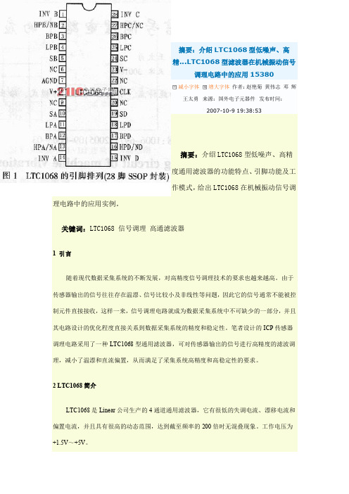
2.1 LTC1068的引脚功能LTC1068采用24引脚PDIP和28引脚SSOP二种封装,引脚排列如图1所示。
各个引脚的功能如下所述:V+、V-:滤波器电源正负输入端。
通常情况下在该引脚与模拟地之间接一个0.1μF的旁路电容器以抗击干扰。
滤波器的供电电源必须与其他数字或模拟电路的高电压电源分离开。
有双端和单端二种供电方式,建议使用低噪声线性电源。
AGND:模拟地。
滤波器的性能很大程度上取决于模拟信号地的质量,单端供电方式时,AGND引脚必须接一个至少0.47μF的旁路电容器。
CLK:时钟信号输入端。
任何TTL或CMOS占空比为50%的方波时钟信号源都可以作为时钟信号的输入。
GS881E18AD-150IT资料

GS881E18/32/36ADSupplemental Datasheet InformationThis supplemental information applies to the GS881E18/36AT datasheet, which you will find attached to this document. This supplement includes a new package offering (the 165-bump BGA—Package D), as well as an additional organization (x32, which is only offered in the 165 BGA for this part).GS881E18/32/36AD Supplemental Datasheet Information165 Bump BGA—x18 Commom I/O—Top View (Package D)1234567891011A NC A E1B B NC E3BW ADSC ADV A A AB NC A E2NC B A CK GW G ADSP A NC BC NC NC V DDQ V SS V SS V SS V SS V SS V DDQ NC DQA CD NC DQB V DDQ V DD V SS V SS V SS V DD V DDQ NC DQA DE NC DQB V DDQ V DD V SS V SS V SS V DD V DDQ NC DQA EF NC DQB V DDQ V DD V SS V SS V SS V DD V DDQ NC DQA FG NC DQB V DDQ V DD V SS V SS V SS V DD V DDQ NC DQA GH FT MCL NC V DD V SS V SS V SS V DD NC NC ZZ HJ DQB NC V DDQ V DD V SS V SS V SS V DD V DDQ DQA NC JK DQB NC V DDQ V DD V SS V SS V SS V DD V DDQ DQA NC KL DQB NC V DDQ V DD V SS V SS V SS V DD V DDQ DQA NC LM DQB NC V DDQ V DD V SS V SS V SS V DD V DDQ DQA NC MN DQB NC V DDQ V SS NC NC NC V SS V DDQ NC NC NP NC NC A A TDI A1TDO A A A A PR LBO NC A A TMS A0TCK A A A A R11 x 15 Bump BGA—13mm x 15 mm Body—1.0 mm Bump PitchGS881E18/32/36AD Supplemental Datasheet Information165 Bump BGA—x32 Common I/O—Top View (Package D)1234567891011A NC A E1BC B B E3BW ADSC ADV A NC AB NC A E2BD B A CK GW G ADSP A NC BC NC NC V DDQ V SS V SS V SS V SS V SS V DDQ NC NC CD DQC DQC V DDQ V DD V SS V SS V SS V DD V DDQ DQB DQB DE DQC DQC V DDQ V DD V SS V SS V SS V DD V DDQ DQB DQB EF DQC DQC V DDQ V DD V SS V SS V SS V DD V DDQ DQB DQB FG DQC DQC V DDQ V DD V SS V SS V SS V DD V DDQ DQB DQB GH FT MCL NC V DD V SS V SS V SS V DD NC NC ZZ HJ DQD DQD V DDQ V DD V SS V SS V SS V DD V DDQ DQA DQA JK DQD DQD V DDQ V DD V SS V SS V SS V DD V DDQ DQA DQA KL DQD DQD V DDQ V DD V SS V SS V SS V DD V DDQ DQA DQA LM DQD DQD V DDQ V DD V SS V SS V SS V DD V DDQ DQA DQA MN NC NC V DDQ V SS NC NC NC V SS V DDQ NC NC NP NC NC A A TDI A1TDO A A A A PR LBO NC A A TMS A0TCK A A A A R11 x 15 Bump BGA—13mm x 15 mm Body—1.0 mm Bump PitchGS881E18/32/36AD Supplemental Datasheet Information165 Bump BGA—x36 Common I/O—Top View (Package D)1234567891011A NC A E1BC B B E3BW ADSC ADV A NC AB NC A E2BD B A CK GW G ADSP A NC BC DQC NC V DDQ V SS V SS V SS V SS V SS V DDQ NC DQB CD DQC DQC V DDQ V DD V SS V SS V SS V DD V DDQ DQB DQB DE DQC DQC V DDQ V DD V SS V SS V SS V DD V DDQ DQB DQB EF DQC DQC V DDQ V DD V SS V SS V SS V DD V DDQ DQB DQB FG DQC DQC V DDQ V DD V SS V SS V SS V DD V DDQ DQB DQB GH FT MCL NC V DD V SS V SS V SS V DD NC NC ZZ HJ DQD DQD V DDQ V DD V SS V SS V SS V DD V DDQ DQA DQA JK DQD DQD V DDQ V DD V SS V SS V SS V DD V DDQ DQA DQA KL DQD DQD V DDQ V DD V SS V SS V SS V DD V DDQ DQA DQA LM DQD DQD V DDQ V DD V SS V SS V SS V DD V DDQ DQA DQA MN DQD NC V DDQ V SS NC NC NC V SS V DDQ NC DQA NP NC NC A A TDI A1TDO A A A A PR LBO NC A A TMS A0TCK A A A A R11 x 15 Bump BGA—13mm x 15 mm Body—1.0 mm Bump PitchGS881E18/32/36ADSupplemental Datasheet InformationGS881E18/32/36AD 165-Bump BGA Pin DescriptionSymbol Type DescriptionA0, A1I Address field LSBs and Address Counter Preset InputsAn I Address InputsA17, A18I Address InputDQ A1–DQ A9DQ B1–DQ B9I/O Data Input and Output pinsDQ C1–DQ C9DQ D1–DQ D9B A, B B, B C, B D I Byte Write Enable for DQ A, DQ B, DQ C, DQ D I/Os; active lowNC—No ConnectCK I Clock Input Signal; active highBW I Byte Write—Writes all enabled bytes; active lowGW I Global Write Enable—Writes all bytes; active lowE1I Chip Enable; active lowE3I Chip Enable; active lowE2I Chip Enable; active highG I Output Enable; active lowADV I Burst address counter advance enable; active l0w ADSC, ADSP I Address Strobe (Processor, Cache Controller); active low ZZ I Sleep mode control; active highFT I Flow Through or Pipeline mode; active lowLBO I Linear Burst Order mode; active lowTMS I Scan Test Mode SelectTDI I Scan Test Data InTDO O Scan Test Data OutTCK I Scan Test ClockMCL—Must Connect LowV DD I Core power supplyV SS I I/O and Core GroundV DDQ I Output driver power supplyGS881E18/32/36ADSupplemental Datasheet InformationPackage Dimensions—165-Bump FPBGA (Package D; Variation 1)A B C D E F G H J K L M N P RA B C D E F G H J K L M N P R1 2 3 4 5 6 7 8 9 10 11 10 9 8 7 6 5 4 3 2A1 TOPA1BOTTOM 1.0 1.010.1.01.014.13±0.015±0.0AB 0.20(4Ø0.10Ø0.25CC A BM M Ø0.40~0.50CSEATING0.15C0.25~0.41.200.45±0.050.25C(0.26GS881E18/32/36ADSupplemental Datasheet InformationOrdering Information OrgPart Number1TypePackageSpeed 2(MHz/ns)T A 3Status512K x 18GS881E18AD-250Pipeline/Flow Through 165 BGA 250/5.5C 512K x 18GS881E18AD-225Pipeline/Flow Through 165 BGA 225/6C 512K x 18GS881E18AD-200Pipeline/Flow Through 165 BGA 200/6.5C 512K x 18GS881E18AD-166Pipeline/Flow Through 165 BGA 166/7C 512K x 18GS881E18AD-150Pipeline/Flow Through 165 BGA 150/7.5C 512K x 18GS881E18AD-133Pipeline/Flow Through 165 BGA 133/8.5C 256K x 32GS881E32AD-250Pipeline/Flow Through 165 BGA 250/5.5C 256K x 32GS881E32AD-225Pipeline/Flow Through 165 BGA 225/6C 256K x 32GS881E32AD-200Pipeline/Flow Through 165 BGA 200/6.5C 256K x 32GS881E32AD-166Pipeline/Flow Through 165 BGA 166/7C 256K x 32GS881E32AD-150Pipeline/Flow Through 165 BGA 150/7.5C 256K x 32GS881E32AD-133Pipeline/Flow Through 165 BGA 133/8.5C 256K x 36GS881E36AD-250Pipeline/Flow Through 165 BGA 250/5.5C 256K x 36GS881E36AD-225Pipeline/Flow Through 165 BGA 225/6C 256K x 36GS881E36AD-200Pipeline/Flow Through 165 BGA 200/6.5C 256K x 36GS881E36AD-166Pipeline/Flow Through 165 BGA 166/7C 256K x 36GS881E36AD-150Pipeline/Flow Through 165 BGA 150/7.5C 256K x 36GS881E36AD-133Pipeline/Flow Through 165 BGA 133/8.5C 512K x 18GS881E18AD-250I Pipeline/Flow Through 165 BGA 250/5.5I 512K x 18GS881E18AD-225I Pipeline/Flow Through 165 BGA 225/6I 512K x 18GS881E18AD-200I Pipeline/Flow Through 165 BGA 200/6.5I 512K x 18GS881E18AD-166I Pipeline/Flow Through 165 BGA 166/7I 512K x 18GS881E18AD-150I Pipeline/Flow Through 165 BGA 150/7.5I 512K x 18GS881E18AD-133I Pipeline/Flow Through 165 BGA 133/8.5I 256K x 32GS881E32AD-250IPipeline/Flow Through165 BGA250/5.5I256K x 32GS881E32AD-225I Pipeline/Flow Through 165 BGA 225/6I Notes:1.Customers requiring delivery in Tape and Reel should add the character “T” to the end of the part number. Example: GS88136AD-100IT.2.The speed column indicates the cycle frequency (MHz) of the device in Pipeline mode and the latency (ns) in Flow Through mode. Eachdevice is Pipeline/Flow Through mode-selectable by the user.3.T A = C = Commercial Temperature Range. T A = I = Industrial Temperature Range.4.GSI offers other versions this type of device in many different configurations and with a variety of different features, only some of whichare covered in this data sheet. See the GSI Technology web site () for a complete listing of current offeringsGS881E18/32/36ADSupplemental Datasheet Information256K x 32GS881E32AD-200I Pipeline/Flow Through 165 BGA 200/6.5I 256K x 32GS881E32AD-166I Pipeline/Flow Through 165 BGA 166/7I 256K x 32GS881E32AD-150I Pipeline/Flow Through 165 BGA 150/7.5I 256K x 32GS881E32AD-133I Pipeline/Flow Through 165 BGA 133/8.5I 256K x 36GS881E36AD-250I Pipeline/Flow Through 165 BGA 250/5.5I 256K x 36GS881E36AD-225I Pipeline/Flow Through 165 BGA 225/6I 256K x 36GS881E36AD-200I Pipeline/Flow Through 165 BGA 200/6.5I 256K x 36GS881E36AD-166I Pipeline/Flow Through 165 BGA 166/7I 256K x 36GS881E36AD-150IPipeline/Flow Through165 BGA150/7.5I256K x 36GS881E36AD-133I Pipeline/Flow Through 165 BGA 133/8.5I Ordering Information OrgPart Number1TypePackageSpeed 2(MHz/ns)T A 3StatusNotes:1.Customers requiring delivery in Tape and Reel should add the character “T” to the end of the part number. Example: GS88136AD-100IT.2.The speed column indicates the cycle frequency (MHz) of the device in Pipeline mode and the latency (ns) in Flow Through mode. Eachdevice is Pipeline/Flow Through mode-selectable by the user.3.T A = C = Commercial Temperature Range. T A = I = Industrial Temperature Range.4.GSI offers other versions this type of device in many different configurations and with a variety of different features, only some of whichare covered in this data sheet. See the GSI Technology web site () for a complete listing of current offeringsGS881E18/36AT-250/225/200/166/150/133512K x 18, 256K x 369Mb Synchronous Burst SRAMs250 MHz –133 MHz 2.5 V or 3.3 V V DD 2.5 V or 3.3 V I/O100-Pin TQFP Commercial Temp Industrial Temp Features• Dual Dycle Deselect (DCD) operation• IEEE 1149.1 JTAG-compatible Boundary Scan • 2.5 V or 3.3 V +10%/–10% core power supply • 2.5 V or 3.3 V I/O supply• LBO pin for Linear or Interleaved Burst mode• Internal input resistors on mode pins allow floating mode pins • Byte Write (BW) and/or Global Write (GW) operation • Internal self-timed write cycle• Automatic power-down for portable applications • JEDEC-standard packageFunctional DescriptionApplicationsThe GS881E18/36AT is a 9,437,184-bit high performance synchronous SRAM with a 2-bit burst address counter. Although of a type originally developed for Level 2 Cache applications supporting high performance CPUs, the device now finds application in synchronous SRAM applications, ranging from DSP main store to networking chip set support. ControlsAddresses, data I/Os, chip enable (E1, E2), address burst control inputs (ADSP, ADSC, ADV) and write control inputs (Bx, BW, GW) are synchronous and are controlled by a positive-edge-triggered clock input (CK). Output enable (G) and power down control (ZZ) are asynchronous inputs. Burst cycles can be initiated with either ADSP or ADSC inputs. In Burst mode, subsequent burst addresses are generated internally and are controlled by ADV. The burst address counter may be configured to count in either linear orinterleave order with the Linear Burst Order (LBO) input. The Burst function need not be used. New addresses can be loaded on every cycle with no degradation of chip performance.Flow Through/Pipeline ReadsThe function of the Data Output register can be controlled by the user via the FT mode pin (Pin 14). Holding the FT mode pin low places the RAM in Flow Through mode, causing output data to bypass the Data Output Register. Holding FT high places the RAM in Pipeline mode, activating the rising-edge-triggered Data Output Register.DCD Pipelined ReadsThe GS881E18/36AT is a DCD (Dual Cycle Deselect)pipelined synchronous SRAM. SCD (Single Cycle Deselect) versions are also available. DCD SRAMs pipeline disable commands to the same degree as read commands. DCD RAMs hold the deselect command for one full cycle and then begin turning off their outputs just after the second rising edge of clock.Byte Write and Global WriteByte write operation is performed by using Byte Write enable (BW) input combined with one or more individual byte write signals (Bx). In addition, Global Write (GW) is available for writing all bytes at one time, regardless of the Byte Write control inputs.Sleep ModeLow power (Sleep mode) is attained through the assertion (High) of the ZZ signal, or by stopping the clock (CK). Memory data is retained during Sleep mode.Core and Interface VoltagesThe GS881E18/36AT operates on a 2.5 V or 3.3 V power supply. All input are 3.3 V and 2.5 V compatible. Separate output power (V DDQ ) pins are used to decouple output noise from the internal circuits and are 3.3 V and 2.5 V compatible.Parameter Synopsis-250-225-200-166-150-133Unit Pipeline 3-1-1-1t KQ tCycle2.54.0 2.74.43.05.0 3.46.0 3.86.74.07.5ns nsCurr (x18)Curr (x36)280330255300230270200230185215165190mA mA Flow Through 2-1-1-1t KQ tCycle5.55.56.06.0 6.56.57.07.07.57.58.58.5ns ns Curr (x18)Curr (x36)175200165190160180150170145165135150mA mAGS881E18/36AT-250/225/200/166/150/133GS881E18A 100-Pin TQFP Pinout (Package T)807978777675747372717069686766656463626160595857565554535251123456789101112131415161718192021222324252627282930V DDQ V SS DQ B DQ B V SS V DDQ DQ B DQ B FT V DD NC V SS DQ B DQ B6V DDQ V SS DQ B DQ B DQP BV SS V DDQ V DDQ V SS DQ A DQ A V SS V DDQ DQ A DQ A V SS NC V DD ZZ DQ A DQ A V DDQ V SS DQ A DQ A V SS V DDQ L B O A 5A AA 1A 0T M S T D I V S SV D DT D O T C K A A A A A AA A E 1E 2N C N C B BB AA C K G WB W V D DV S SG A D S C A D S P A D V A AA 512K x 18Top View DQP A A NC NC NC NC NC NC NC NCNC NC NC NC NC NC NCNC NC 100999897969594939291908988878685848382813132333435363738394041424344454647484950GS881E18/36AT-250/225/200/166/150/133GS881E36A 100-Pin TQFP Pinout (Package T)807978777675747372717069686766656463626160595857565554535251123456789101112131415161718192021222324252627282930V DDQ V SS DQ C DQ C V SS V DDQ DQ C DQ C FT V DD NC V SS DQ D DQ D V DDQ V SS DQ D DQ D DQ D V SS V DDQ V DDQ V SS DQ B DQ B V SS V DDQ DQ B DQ B V SS NC V DD ZZ DQ A DQ A V DDQ V SS DQ A DQ A V SS V DDQ L B O A A A A A 1A 0V S SV D DA A A A A AA A E 1E 2B DB CB BB AA C K G WB W V D DV S SG A D S C A D S P A D V A AA 256K x 36Top View DQB DQP B DQ B DQ B DQ B DQ A DQ A DQ A DQ A DQP ADQ C DQ C DQ C DQ D DQ D DQ D DQP DDQ C DQP C 100999897969594939291908988878685848382813132333435363738394041424344454647484950T M S T D I T D O T C KGS881E18/36AT-250/225/200/166/150/133TQFP Pin DescriptionSymbol Type DescriptionA0, A1I Address field LSBs and Address Counter preset InputsA n I Address InputsDQ ADQ BI/O Data Input and Output pinsDQ CDQ DNC—No ConnectBW I Byte Write—Writes all enabled bytes; active lowB A, B B, B C, B D I Byte Write Enable for DQ A, DQ B Data I/Os; active lowCK I Clock Input Signal; active highGW I Global Write Enable—Writes all bytes; active lowE1I Chip Enable; active lowE2I Chip Enable; active highG I Output Enable; active lowADV I Burst address counter advance enable; active low ADSP, ADSC I Address Strobe (Processor, Cache Controller); active low ZZ I Sleep Mode control; active highTMS I Scan Test Mode SelectTDI I Scan Test Data InTDO O Scan Test Data OutTCK I Scan Test ClockFT I Flow Through or Pipeline mode; active lowLBO I Linear Burst Order mode; active lowV DD I Core power supplyV SS I I/O and Core GroundV DDQ I Output driver power supplyGS881E18/36AT-250/225/200/166/150/133GS881E18/36A Block DiagramA1A0A0A1D0D1Q1Q0Counter LoadD QDQRegisterRegisterDQRegisterDQRegisterDQRegisterD QRegisterD QRegisterD QRegisterD QR e g i s t e rDQ RegisterA0–AnLBO ADV CK ADSC ADSP GW BW E 1FT GZZPower Down ControlMemory Array36364AQD DQx1–DQx9NCParity NCParity EncodeCompare3643636432Note: Only x36 version shown for simplicity.13636DQR e g i s t e r 4B AB BB CB DGS881E18/36AT-250/225/200/166/150/133Note:There are pull-up devices on the ZQ and FT pins and a pull-down device on the ZZ pin, so those input pins can be unconnected and the chip will operate in the default states as specified in the above tables.Burst Counter SequencesBPR 1999.05.18Mode Pin FunctionsMode NamePin NameStateFunctionBurst Order Control LBO L Linear Burst H Interleaved Burst Output Register Control FT L Flow Through H or NC Pipeline Power Down ControlZZL or NC Active HStandby, I DD = I SBNote:The burst counter wraps to initial state on the 5th clock.Note:The burst counter wraps to initial state on the 5th clock.Linear Burst SequenceA[1:0]A[1:0]A[1:0]A[1:0]1st address 000110112nd address 011011003rd address 101100014th address11000110Interleaved Burst SequenceA[1:0]A[1:0]A[1:0]A[1:0]1st address 000110112nd address 010011103rd address 101100014th address11100100GS881E18/36AT-250/225/200/166/150/1331.All byte outputs are active in read cycles regardless of the state of Byte Write Enable inputs.2.Byte Write Enable inputs B A , B B , B C and/or B D may be used in any combination with BW to write single or multiple bytes.3.All byte I/Os remain High-Z during all write operations regardless of the state of Byte Write Enable inputs.4.Bytes “C ” and “D ” are only available on the x36 version.Byte Write Truth TableFunctionGWBWB AB BB CB DNotesRead H H X X X X 1Read H L H H H H 1Write byte a H L L H H H 2, 3Write byte b H L H L H H 2, 3Write byte c H L H H L H 2, 3, 4Write byte d H L H H H L 2, 3, 4Write all bytesHLLLLL2, 3, 4Write all bytes L X X X X XGS881E18/36AT-250/225/200/166/150/133 Synchronous Truth TableOperation Address UsedStateDiagramKey5E1ADSP ADSC ADV W3DQ4Deselect Cycle, Power Down None X H X L X X High-Z Read Cycle, Begin Burst External R L L X X X Q Read Cycle, Begin Burst External R L H L X F Q Write Cycle, Begin Burst External W L H L X T D Read Cycle, Continue Burst Next CR X H H L F Q Read Cycle, Continue Burst Next CR H X H L F Q Write Cycle, Continue Burst Next CW X H H L T D Write Cycle, Continue Burst Next CW H X H L T D Read Cycle, Suspend Burst Current X H H H F Q Read Cycle, Suspend Burst Current H X H H F Q Write Cycle, Suspend Burst Current X H H H T D Write Cycle, Suspend Burst Current H X H H T D Notes:1.X = Don’t Care, H = High, L = Low2.W = T (True) and F (False) is defined in the Byte Write Truth Table preceding.3.G is an asynchronous input. G can be driven high at any time to disable active output drivers. G low can only enable active drivers (shownas “Q” in the Truth Table above).4.All input combinations shown above are tested and supported. Input combinations shown in gray boxes need not be used to accomplishbasic synchronous or synchronous burst operations and may be avoided for simplicity.5.Tying ADSP high and ADSC low allows simple non-burst synchronous operations. See BOLD items above.6.Tying ADSP high and ADV low while using ADSC to load new addresses allows simple burst operations. See ITALIC items above.GS881E18/36AT-250/225/200/166/150/133Simplified State DiagramFirst WriteFirst ReadBurst WriteBurst ReadDeselect R WCRCWX XWRRWRXXX S i m p l e S y n c h r o n o u s O p e r a t i o nS i m p l e B u r s t S y n c h r o n o u s O p e r a t i o nCR RCWCRCRNotes:1.The diagram shows only supported (tested) synchronous state transitions. The diagram presumes G is tied low.2.The upper portion of the diagram assumes active use of only the Enable (E1) and Write (B A , B B , B C , B D , BW, and GW) control inputs, andthat ADSP is tied high and ADSC is tied low.3.The upper and lower portions of the diagram together assume active use of only the Enable, Write, and ADSC control inputs, andassumes ADSP is tied high and ADV is tied low.GS881E18/36AT-250/225/200/166/150/133Simplified State Diagram with GFirst WriteFirst ReadBurst WriteBurst ReadDeselect R WCRCWXXWRRWRXXX CRR CW CRCRW CWW CWNotes:1.The diagram shows supported (tested) synchronous state transitions plus supported transitions that depend upon the use of G.e of “Dummy Reads” (Read Cycles with G High) may be used to make the transition from read cycles to write cycles without passingthrough a deselect cycle. Dummy read cycles increment the address counter just like normal read cycles.3.Transitions shown in gray tone assume G has been pulsed high long enough to turn the RAM’s drivers off and for incoming data to meetData Input Set Up Time.GS881E18/36AT-250/225/200/166/150/133Note:Permanent damage to the device may occur if the Absolute Maximum Ratings are exceeded. Operation should be restricted to Recommended Operating Conditions. Exposure to conditions exceeding the Absolute Maximum Ratings, for an extended period of time, may affect reliability of this component.Absolute Maximum Ratings(All voltages reference to V SS )SymbolDescriptionValueUnitV DD Voltage on V DD Pins –0.5 to 4.6V V DDQ Voltage in V DDQ Pins –0.5 to 4.6V V I/O Voltage on I/O Pins –0.5 to V DDQ +0.5 (≤ 4.6 V max.)V V IN Voltage on Other Input Pins –0.5 to V DD +0.5 (≤ 4.6 V max.)V I IN Input Current on Any Pin +/–20mA I OUT Output Current on Any I/O Pin +/–20mA P D Package Power Dissipation 1.5WT STG Storage Temperature –55 to 125o C T BIASTemperature Under Bias–55 to 125oCPower Supply Voltage RangesParameterSymbolMin.Typ.Max.UnitNotes3.3 V Supply Voltage V DD3 3.0 3.3 3.6V 2.5 V Supply Voltage V DD2 2.3 2.5 2.7V 3.3 V V DDQ I/O Supply Voltage V DDQ3 3.0 3.3 3.6V 2.5 V V DDQ I/O Supply VoltageV DDQ22.32.52.7VNotes:1.The part numbers of Industrial Temperature Range versions end the character “I”. Unless otherwise noted, all performance specifica-tions quoted are evaluated for worst case in the temperature range marked on the device.2.Input Under/overshoot voltage must be –2 V > Vi < V DDn +2 V not to exceed 4.6 V maximum, with a pulse width not to exceed 20% tKC.GS881E18/36AT-250/225/200/166/150/133V DDQ3 Range Logic LevelsParameter Symbol Min.Typ.Max.Unit Notes V DD Input High Voltage V IH 2.0—V DD + 0.3V1V DD Input Low Voltage V IL–0.3—0.8V1V DDQ I/O Input High Voltage V IHQ 2.0—V DDQ + 0.3V1,3V DDQ I/O Input Low Voltage V ILQ–0.3—0.8V1,3 Notes:1.The part numbers of Industrial Temperature Range versions end the character “I”. Unless otherwise noted, all performance specifica-tions quoted are evaluated for worst case in the temperature range marked on the device.2.Input Under/overshoot voltage must be –2 V > Vi < V DDn+2 V not to exceed 4.6 V maximum, with a pulse width not to exceed 20% tKC.3.V IHQ (max) is voltage on V DDQ pins plus 0.3 V.V DDQ2 Range Logic LevelsParameter Symbol Min.Typ.Max.Unit Notes V DD Input High Voltage V IH0.6*V DD—V DD + 0.3V1V DD Input Low Voltage V IL–0.3—0.3*V DD V1V DDQ I/O Input High Voltage V IHQ0.6*V DD—V DDQ + 0.3V1,3V DDQ I/O Input Low Voltage V ILQ–0.3—0.3*V DD V1,3 Notes:1.The part numbers of Industrial Temperature Range versions end the character “I”. Unless otherwise noted, all performance specifica-tions quoted are evaluated for worst case in the temperature range marked on the device.2.Input Under/overshoot voltage must be –2 V > Vi < V DDn+2 V not to exceed 4.6 V maximum, with a pulse width not to exceed 20% tKC.3.V IHQ (max) is voltage on V DDQ pins plus 0.3 V.Recommended Operating TemperaturesParameter Symbol Min.Typ.Max.Unit Notes Ambient Temperature (Commercial Range Versions)T A02570°C2 Ambient Temperature (Industrial Range Versions)T A–402585°C2 Notes:1.The part numbers of Industrial Temperature Range versions end the character “I”. Unless otherwise noted, all performance specifica-tions quoted are evaluated for worst case in the temperature range marked on the device.2.Input Under/overshoot voltage must be –2 V > Vi < V DDn+2 V not to exceed 4.6 V maximum, with a pulse width not to exceed 20% tKC.GS881E18/36AT-250/225/200/166/150/133Note:These parameters are sample tested.Capacitance(T A = 25o C, f = 1 MH Z , V DD = 2.5 V)ParameterSymbolTest conditionsTyp.Max.UnitInput Capacitance C IN V IN = 0 V 45pF Input/Output Capacitance C I/OV OUT = 0 V67pFAC Test ConditionsParameterConditionsInput high level V DD – 0.2 V Input low level 0.2 V Input slew rate 1 V/ns Input reference level V DD /2Output reference levelV DDQ /2Output loadFig. 1Notes:1.Include scope and jig capacitance.2.Test conditions as specified with output loading as shown in Fig. 1unless otherwise noted.3.Device is deselected as defined by the Truth Table. 50% tKCV SS – 2.0 V50%V SS V IHUndershoot Measurement and TimingOvershoot Measurement and Timing50% tKCV DD + 2.0 V50%V DDV ILDQV DDQ/250Ω30pF *Output Load 1* Distributed Test Jig CapacitanceGS881E18/36AT-250/225/200/166/150/133DC Electrical CharacteristicsParameter Symbol Test Conditions Min Max Input Leakage Current(except mode pins)I IL V IN = 0 to V DD–1 uA 1 uAZZ Input Current I IN1V DD≥V IN ≥V IH0 V≤ V IN ≤ V IH–1 uA–1 uA1 uA100 uAFT Input Current I IN2V DD≥V IN ≥V IL0 V≤ V IN ≤ V IL–100 uA–1 uA1 uA1 uAOutput Leakage Current I OL Output Disable, V OUT = 0 to V DD–1 uA 1 uA Output High Voltage V OH2I OH = –8 mA, V DDQ = 2.375 V 1.7 V—Output High Voltage V OH3I OH = –8 mA, V DDQ = 3.135 V 2.4 V—Output Low Voltage V OL I OL = 8 mA—0.4 VGS881E18/36AT-250/225/200/166/150/133N o t e s : 1.I D D a n d I D D Q a p p l y t o a n y c o m b i n a t i o n o f V D D 3, V D D 2, V D D Q 3, a n d V D D Q 2 o p e r a t i o n .2.A l l p a r a m e t e r s l i s t e d a r e w o r s t c a s e s c e n a r i o .O p e r a t i n g C u r r e n t sP a r a m e t e r T e s t C o n d i t i o n s M o d eS y m b o l -250-225-200-166-150-133U n i t0t o 70°C –40 t o 85°C0t o 70°C–40 t o 85°C 0t o 70°C –40t o 85°C 0 t o 70°C –40t o 85°C 0 t o 70°C –40t o 85°C 0 t o 70°C –40t o 85°C O p e r a t i n g C u r r e n tD e v i c e S e l e c t e d ; A l l o t h e r i n p u t s ≥V I H o r ≤ V I LO u t p u t o p e n(x 36)P i p e l i n eI D DI D D Q290403004026535275352403025030205252152519025200251702018020m AF l o w T h r o u g hI D DI D D Q180201902017020180201651517515155151651515015160151401015010m A(x 18)P i p e l i n eI D DI D D Q260202702023520245202151522515185151951517015180151551016510m AF l o w T h r o u g hI D DI D D Q165101751015510165101501016010140101501013510145101251013510m AS t a n d b y C u r r e n tZ Z ≥ V D D – 0.2 V—P i p e l i n eI S B 203020302030203020302030m AF l o w T h r o u g hI S B203020302030203020302030m AD e s e l e c t C u r r e n tD e v i c e D e s e l e c t e d ; A l l o t h e r i n p u t s ≥ V I H o r ≤ V I L—P i p e l i n eI D D859080857580647060655055m AF l o w T h r o u g hI D D606560655055505550554550m AGS881E18/36AT-250/225/200/166/150/133Notes:1.These parameters are sampled and are not 100% tested2.ZZ is an asynchronous signal. However, In order to be recognized on any given clock cycle, ZZ must meet the specified setup and holdtimes as specified above.AC Electrical CharacteristicsParameter Symbol -250-225-200-166-150-133Unit Min Max Min Max Min Max Min Max Min Max Min Max PipelineClock Cycle Time tKC 4.0— 4.4— 5.0— 6.0— 6.7—7.5—ns Clock to Output Valid tKQ — 2.5— 2.7— 3.0— 3.4— 3.8— 4.0ns Clock to Output InvalidtKQX 1.5— 1.5— 1.5— 1.5— 1.5— 1.5—ns Clock to Output in Low-ZtLZ 1 1.5— 1.5— 1.5— 1.5— 1.5— 1.5—ns Setup time tS 1.2— 1.3— 1.4— 1.5— 1.5— 1.5—ns Hold time tH 0.2—0.3—0.4—0.5—0.5—0.5—ns Flow ThroughClock Cycle Time tKC 5.5— 6.0— 6.5—7.0—7.5—8.5—ns Clock to Output ValidtKQ — 5.5— 6.0— 6.5—7.0—7.5—8.5ns Clock to Output Invalid tKQX 3.0— 3.0— 3.0— 3.0— 3.0— 3.0—ns Clock to Output in Low-ZtLZ 1 3.0— 3.0— 3.0— 3.0— 3.0— 3.0—ns Setup time tS 1.5— 1.5— 1.5— 1.5— 1.5— 1.5—ns Hold time tH 0.5—0.5—0.5—0.5—0.5—0.5—ns Clock HIGH Time tKH 1.3— 1.3— 1.3— 1.3— 1.5— 1.7—ns Clock LOW Time tKL 1.5—1.5—1.5—1.5— 1.7—2—ns Clock to Output inHigh-Z tHZ 1 1.5 2.3 1.5 2.5 1.5 3.0 1.5 3.0 1.5 3.0 1.5 3.0ns G to Output Valid tOE — 2.3— 2.5— 3.2— 3.5— 3.8— 4.0ns G to output in Low-Z tOLZ 10—0—0—0—0—0—ns G to output in High-Z tOHZ 1— 2.3— 2.5— 3.0— 3.0— 3.0— 3.0ns ZZ setup time tZZS 25—5—5—5—5—5—ns ZZ hold time tZZH 21—1—1—1—1—1—ns ZZ recoverytZZR20—20—20—20—20—20—ns。
LT1084MK-12中文资料

FRONT VIEW
3 2 1
P PACKAGE 3-LEAD TO-3P PLASTIC
θJA = 45°C/W
ORDER PART NUMBER
VIN
LT1083CP-5 LT1083CP-12
VOUT
LT1084CP-5
GND
LT1084CP-12
TAB IS OUTPUT
FRONT VIEW
Power Dissipation............................... Internally Limited Input Voltage (Note 1) ............................................. 30V Operating Input Voltage
LT1083/84/85 Fixed
ELECTRICAL CHARACTERISTICS
PARAMETER Output Voltage
Line Regulation
CONDITIONS LT1085-3.6
LT1083/4/5-5 LT1083/4/5-12 LT1084-3.3
5V ≤ VIN ≤ 15V, 0 ≤ IOUT ≤ 2.5A (Note 8) VIN = 4.75V, IOUT = 3A, TJ ≥ 0°C VIN = 4.75V, IOUT = 2.5A, TJ ≥ 0°C VIN = 4.75V, IOUT = 1.5A, TJ > 0°C
UL1081中文

UL1081游泳池PUMP、过滤器、氯化器标准内容前言介绍1、范围---------------------------------- ----------------------------------------32、概要---------------------------------------------------------------------------33、术语表------------------------------------------------------------------------3结构4、围护框架---------------------------------------------------------------------45、机械装配------------------------------------------------------------------10A6、易接近的未绝缘有电部件、薄膜涂层金属线、可动部件--------117、维修预备--------------------------------------------------------------------158、抗腐蚀------------------------------------------------------------------------159、电源供给连结、线、插接单元----------------------------------------- 1710、电源供给连结---永久连接单元-----------------------------------------1911、接地--------------------------------------------------------------------------2112、带电部件--------------------------------------------------------------------2313、内部金属线-----------------------------------------------------------------2314、双层绝缘--------------------------------------------------------------------2415、接合--------------------------------------------------------------------------2516、分离电路--------------------------------------------------------------------2517、绝缘材料--------------------------------------------------------------------2618、间距--------------------------------------------------------------------------2619、内套管-----------------------------------------------------------------------2920、垫圈--------------------------------------------------------------------------2921、降低人身伤害的风险-----------------------------------------------------2922、部件受水压-----------------------------------------------------------------3023、马达--------------------------------------------------------------------------3024、过载保护装置--------------------------------------------------------------3125、开关与控制-----------------------------------------------------------------3126、电容器-----------------------------------------------------------------------3227、灯架插头与电工插座-----------------------------------------------------3228、电解氯化器-----------------------------------------------------------------32性能29、概要--------------------------------------------------------------------------3330、漏电测试--------------------------------------------------------------------3331、起动电流测试--------------------------------------------------------------3632、输入电流测试--------------------------------------------------------------3633、接地连续性测试---------------------------------------------------------36A34、温度测试--------------------------------------------------------------------3735、耐压测试--------------------------------------------------------------------4136、马达过电流保护电路测试-----------------------------------------------4337、泼水测试--------------------------------------------------------------------4438、抗紫外线和水测试--------------------------------------------------------4739、抗冲击测试-------------------------------------------------------------------5140、垫圈老化测试----------------------------------------------------------------5241、反常操作测试----------------------------------------------------------------5242、静水力学压力测试----------------------------------------------------------5243、电线夹拉力测试--------------------------------------------------------------5244、开关测试-----------------------------------------------------------------------5345、电镀层金属厚度测试--------------------------------------------------------5346、蠕变测试-----------------------------------------------------------------------55制造业生产线测试47、接地连续性测试--------------------------------------------------------------5548、耐压测试-----------------------------------------------------------------------55额定值49、电线和插接单元--------------------------------------------------------------5650、永久接线单元-----------------------------------------------------------------56标记51、详细资料-----------------------------------------------------------------------5652、耐久性--------------------------------------------------------------------------59介绍53、概要-----------------------------------------------------------------------------60附录A构件标准-------------------------------------------------------------------------------------A11、范围1.1这些要求应用于游泳池、SPA、热澡盆的无监督的PUMP马达、PUMP过滤器组合和氯化器,被用于与NECNFPA 70相一致。
- 1、下载文档前请自行甄别文档内容的完整性,平台不提供额外的编辑、内容补充、找答案等附加服务。
- 2、"仅部分预览"的文档,不可在线预览部分如存在完整性等问题,可反馈申请退款(可完整预览的文档不适用该条件!)。
- 3、如文档侵犯您的权益,请联系客服反馈,我们会尽快为您处理(人工客服工作时间:9:00-18:30)。
12A UG WA WUW A R BSOLUTEXI TI SSupply Voltage (V CC ).................................................6V V +...........................................................................................12V V –....................................................................................... –12V Input VoltageDriver ...........................................................V – to V +Receiver .................................................–30V to 30V ON/OFF Pin..............................................GND to 12V Output VoltageDriver .................................(V – + 30V) to (V + – 30V)Receiver ..................................–0.3V to (V CC + 0.3V)Short-Circuit DurationV +......................................................................................30 sec V –......................................................................................30 sec Driver Output...............................................Indefinite Receiver Output...........................................Indefinite Operating Temperature RangeLT1080C/LT1081C ................................. 0°C to 70°C LT1080I/LT1081I................................ –40°C to 85°C LT1080M/LT1081M.......................... –55°C to 125°C Storage Temperature Range..................–65°C to 150°C Lead Temperature (Soldering, 10 sec)................. 300°CWUUPACKAGE/ORDER I FOR ATIO(Note 1)34PI FU CTIO SU U U(Pin numbers refer to LT1080)TEMPERATURE (°C)–55–25025*******125D R I VE R O U T P U T V O L T A G E (V )1080/81 G011086420–2–4–6–8–10TIME (ms)0.20.40.60.8 1.0 1.2 1.4 1.6 1.8 2.0S U P P L Y VO L T A G E (V )1080/81 G031086420–2–4–6–8–10OUTPUT CURRENT (mA)2468101214161820O U T P U T V O LT A G E (V )1080/81 G021086420–2–4–6–8–10Driver Output VoltageSupply Generator OutputsSupply Generation from V CC or ShutdownC1+; C1–; C2+; C2– (Pins 2, 4, 5, 6): Requires an external capacitor (≥1µF) from C1+ to C1– and another from C2+to C2–. Pin 2 can be used for connecting a second positive supply. When a separate positive supply is used, C1 can be deleted.V + (Pin 3): Positive Supply for RS232 Drivers.V + ≈ 2V CC – 1.5V. Requires an exterenal capacitor (≥1µF)for charge storage. May be loaded (up to 15mA) for external system use. Loading does reduce V + voltage (see graphs). Capacitor may be tied to ground or +5V input supply. With multiple transceivers, the V + and V – pins may be paralleled into common capacitors.V – (Pin 7): Negative Supply for RS232 Drivers.V – ≈ –(2V CC – 2.5V). Requires an ex ternal capacitor (≥1µF) for charge stroage. May be loaded (up to –15mA)for external system use. Loading does reduce V – voltage (see graphs). With multiple transceivers, the V + and V –pins may be paralleled into common capacitors.TR2 OUT; TR1 OUT (Pins 8, 15): Driver Outputs with RS232 Voltage Levels. Outputs are in a high impedance state when in the SHUTDOWN mode or when power is off (V CC = 0V) to allow data line sharing. Outputs are fully short-circuit protected from (V – + 30V) to (V + – 30V) with power on, off or in the SHUTDOWN mode. Typical output breakdowns are greater than ±45V and higher appliedvoltages will not damage the device if moderately current limited. Shorting one output will affect output from the other.REC2 IN; REC1 IN (Pins 9, 14): Receiver Inputs. Accepts RS232 voltage levels (±30V) and has 0.4V of hysteresis to provide noise immunity. Input impedance is nominally 5k Ω.REC2 OUT; REC1 OUT (Pins 10, 13): Receiver Outputs with TTL/CMOS Voltage Levels. Outputs are in a high impedance state when in the SHUTDOWN mode to allow data line sharing. Outputs are fully short-circuit protected to ground or V CC with power on, off or in the SHUTDOWN mode.TR2 IN; TR1 IN (Pins 11, 12): RS232 Driver Input Pins.Inputs are TTL/CMOS compatible. Inputs should not be allowed to float. Tie unused inputs to V CC .GND (Pin 16): Ground Pin.V CC (Pin 17): Input Supply Pin. Supply current drops to zero in the SHUTDOWN mode.ON/OFF (Pin 18): Contols the operation mode of the LT1080 and is TTL/CMOS compatible. A logic low puts the device in the SHUTDOWN mode which reduces input supply current to zero and places both driver and receiver outputs in a high impedance state. A logic high fully enables the device.TYPICAL PERFOR A CE CHARACTERISTICSU W56APPLICATIO S I FOR ATIOW UUU The driver output stage of the LT1080 offers significantly improved protection over older bipolar and CMOS de-signs. In addition to current limiting, the driver output can be externally forced to ±30V with no damage or excessive current flow, and will not disrupt the supplies. Some drivers have diodes connected between the outputs and the supplies, so ex ternally applied voltages can cause excessive supply voltage to develop.Placing the LT1080 in the SHUTDOWN mode (Pin 18 low)puts both the driver and receiver outputs in a high imped-ance state. This allows data line sharing and transceiver applications.The SHUTDOWN mode also drops input supply current (V CC ; Pin 17) to zero for power-conscious systems.RS232TRANSMIT/RECEIVE LINE30V1080/81 F01LT1080/LT1081 DriverTransceiverSharing a Receiver LineSharing a Transmitter LineOlder RS232 Drivers and CMOS Drivers+1080/81 F02LOGIC OUTPUTRS232TRANSMISSION LINE7PACKAGE DESCRIPTIO U Dimensions in inches (millimeters) unless otherwise noted.J Package16-Lead CERDIP (Narrow 0.300, Hermetic)(LTC DWG # 05-08-1110)J16 1197J Package18-Lead CERDIP (Narrow 0.300, Hermetic)(LTC DWG # 05-08-1110)8J18 1197910PACKAGE DESCRIPTIOUDimensions in inches (millimeters) unless otherwise noted.SW Package16-Lead Plastic Small Outline (Wide 0.300)(LTC DWG # 05-08-1620)S16 (WIDE) 0396NOTE 1TYPNOTE:1. PIN 1 IDENT, NOTCH ON TOP AND CAVITIES ON THE BOTTOM OF PACKAGES ARE THE MANUFACTURING OPTIONS. THE PART MAY BE SUPPLIED WITH OR WITHOUT ANY OF THE OPTIONSDIMENSION DOES NOT INCLUDE MOLD FLASH. MOLD FLASH SHALL NOT EXCEED 0.006" (0.152mm) PER SIDEDIMENSION DOES NOT INCLUDE INTERLEAD FLASH. INTERLEAD FLASH SHALL NOT EXCEED 0.010" (0.254mm) PER SIDE***11LT1080/LT1081Information furnished by Linear Technology Corporation is believed to be accurate and reliable.However, no responsibility is assumed for its use. Linear Technology Corporation makes no represen-tation that the interconnection of its circuits as described herein will not infringe on existing patent rights.12LT1080/LT108110801fd LT/TP 0400 2K REV D • PRINTED IN USALinear Technology Corporation1630 McCarthy Blvd., Milpitas, CA 95035-7417(408) 432-1900 q FAX: (408) 434-0507 q © LINEAR TECHNOLOGY CORPORATION 1991TYPICAL APPLICATIOUSupporting an LT1039 (Triple Driver/Receiver)11*IN APPLICATIONS WHERE A SEPARATE SECOND POSITIVE SUPPLY IS AVAILABLE (SUCH AS 5V AND 12V), THE 12V SUPPLY MAY BE CONNECTED TO PIN 2 ANDC1 DELETED. THE POWER SUPPLY CIRCUITRY WILL THEN INVERT THE 12V SUPPLY. THE 5V SUPPLY IS STILL NEEDED TO POWER THE BIASING CIRCUITRY AND RECEIVERS.PART NUMBER DESCRIPTIONCOMMENTSLT1180A/LT1181A 5V Low Power 2DR/2TX RS232 Transceiver 0.1µF Capacitors, 10kV ESD LT1780/LT17815V Low Power 2DR/2TX RS232 Transceiver 15kV ESDLT13815V Low Power 2DR/2TX RS232 Transceiver 16-Pin Narrow SO Package LT1130A/LT1140A 5V RS232 TransceiversUp to 5DR/5RXLTC13835V Low Power 2DR/2RX RS232 Transceiver Low Supply Current I CC = 220µA LTC13863.3V Low Power EIA/TIA562 TransceiverLow Supply Current I CC = 200µARELATED PARTS。