OCP8122应用信息 V1.1
CS8122_ch_v1.1
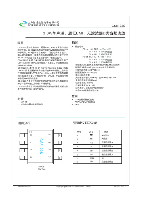
Copyright@Chipstar Microelectronics page 8
www .chipstar -ic .com Mar,2012Rev1.1
效率
输出晶体管的开关工作方式决定了D 类放大器的高效率。
在D类放大器重,输出晶体管就像是一个电流调整开关,切换过程中消耗的额外功率基本可以忽略不计。
输出级相关的功率损耗主要是由MOSFET 导通电阻与电源
CS8122S 无需滤波器的PWM 调制结构减少了外部元件数
目,PCB 面积和系统成本,并且简化了设计。
芯片内置了过流保护,过热保护盒欠压保护功能,这些功能保证了芯片在异常的工作条件下关断芯片,有效地保护了芯片不被损坏,当异常条件消除后,CS8122S 有自恢复功能可以让芯片重新工作。
EMI 测试频谱图
FCC Part 15 Class B。
V8A02解决方案用户手册V2.1

V8A02解决方案用户手册V2.1目录1. 文档说明 (6)1.1版本说明 (6)1.2专有名词 (6)2. 方案简介 (8)2.1方案概述 (8)2.2 功能特点 (8)2.2.1 支持DVI数据源输入 (8)2.2.2 支持宽屏等多种DVI输入分辨率 (8)2.2.3 发送卡超大带载 (8)2.2.4 功能强大的配套软件 (8)2.2.5 智能在线检测 (8)2.2.6 高刷新频率 (8)2.2.7 高灰度等级 (9)2.2.8 支持各种像素类型 (9)2.2.9 灵活支持各种模组 (9)2.2.10 多样的端口设置功能 (9)2.2.11箱体色度调整 (9)2.2.12 逐点校正功能 (9)2.2.13 集成测试功能 (9)2.2.14 联机配置数据 (9)2.2.15 智能维修 (10)2.2.16 环路备份功能 (10)2.2.17 在线升级固件安全可靠 (10)2.2.18 支持低电压输入 (10)2.2.19 配备指示灯及控制面板接口 (10)2.2.20 支持远距离传输 (10)2.2.21 支持音频传输及电源控制 (10)2.2.22 提供完整的二次开发接口 (10)2.2.24 支持内建PWM恒流 (10)2.2.25 支持低亮度高保真 (10)2.3产品清单 (11)3. 应用概述 (12)3.1 典型应用 (12)3.2 环路备份 (13)3.3 多发送卡 (14)4. 功能详解 (15)4.1 模组支持能力 (15)4.1.1 模组行、列数1~128以内任意 (16)4.1.2 模组数据类型 (16)4.1.3 模组内每扫描串移长度 (17)4.1.4 虚拟模组LED灯点位置多种排列方式 (17)4.2 箱体连接设置 (17)4.2.1 箱体内模组级联方式 (17)4.2.2 端口扩展 (18)4.2.3 端口对开 (19)4.2.4 端口逆序 (20)4.2.5 端口偏移 (20)4.2.6 箱体带载高度、宽度 (20)4.2.7 箱体显示起始的行、列位置 (21)4.2.8 箱体无信号输入时显示内容设置 (21)4.2.9 箱体级联数量 (21)4.2.10 箱体色度调整 (21)4.2.11 箱体逐点色度校正 (22)4.2.12 箱体测试功能 (22)4.3 屏体参数调节 (23)4.3.1 多个LED屏设置 (23)4.3.3 虚拟LED屏的实效果 (24)4.3.4 LED屏亮度调节 (25)4.3.5 LED屏对比度调节 (26)4.3.6 LED屏色温调节 (26)4.3.7 关闭LED屏显示 (27)4.3.8 锁定LED屏内容 (27)4.3.9 LED屏环境监控 (27)4.4 显示性能参数说明 (30)4.4.1 灰度等级 (30)4.4.2 刷新频率 (31)4.4.3 亮度效率 (31)4.4.4 最小OE (31)4.5 发送卡带载 (31)4.6 在线检测 (34)4.7 系统升级 (34)4.8 智能维修 (36)4.8.1 接收卡更换 (36)4.8.2模组替换 (37)5. 使用说明 (39)5.1 连接硬件 (39)5.1.1 发送卡安装方法 (39)5.1.2 接收卡安装方法 (39)5.1.3 多功能卡安装方法 (39)5.2 安装软件 (40)5.2.1 配置要求 (40)5.2.2 安装步骤 (40)5.3 系统设置 (40)5.3.1 显卡设置 (40)5.3.2系统设置 (43)6. 附录 (55)6.1 设备推荐型号 (55)6.1.1 DVI复制器 (55)6.2 选用线缆清单 (55)6.2.1 HDMI转DVI线缆 (55)6.2.2 音频线 (56)6.2.3 双绞线 (56)6.2.4 光纤 (56)1. 文档说明1.1版本说明版本日期说明V2.0 2013-01-09 升级自1.71版本V2.1 2013-07-15 新增接收卡产品1.2专有名词以下是本文中使用的专用术语及解释,便于读者更好的理解文章内容。●软件一系列按照特定顺序组织的计算机数据和指令的集合,本文中特指在计算机上运行的应用软件。
泓格科技数据采集卡A812快速指南

5
在启动计算机,进入 Windows 后继续进行下一步骤。
……………………………………………… 新增硬件装置
Windows 2000/XP/2003/Vista32 的使用者需进行此步骤, Windows9x/ME/NT 的使用者请省略此步骤。
7. 新增硬件
7-1 单击“开始 / 设定 / 控制台” 来开启控制台。 7-2 双击“新增/移除硬件”并且按 “下一步>” 按钮。 7-3 选择“是的,我已连接硬件 并且按“下一步 >”按钮。 7-4 选择 “新增硬件装置” 并且按 “下一步 >” 按钮。 7-5 选择 “安装我从清单中手动选取的硬件(高级选项)” 并且按
自我测试
1. 使用 CA-2002(选购) 将 CN4 连接至 CN5。
CN4 CN1 CN5
CN3 CN2
2. 执行 A-812 范例程序。
程序路径(默认):
C:\DAQPro\A812 Win xxx\DEMO
6
ICP DAS A-812PG 用户手册 Version 1.2
3. 确认板卡数量及 DIO 测试。
8. 修改装置属性
2. 1. 选择 Input/Output Range
按下“Change Setting” 改变 I/O Range (此设定值须与 I/O 地 址设定相符)
3. 选择 Interrupt Request
No devices are conflicting
按下 “Change Setting” 改变 Interrupt Request. (此设定值须与 中断资源设定相符)
A7 ON ON ON ON : ON : OFF A6 ON ON ON ON : ON : OFF A5 ON ON OFF OFF : ON : OFF A4 ON OFF ON OFF : ON :
CAN -8123 CAN -8223 CAN -8423 CAN -8823 快速启动用户指南说明
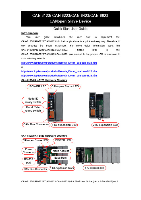
Quick Start User GuideIntroductionThisuserguideintroducestheuserhowtoimplementtheCAN-8123/CAN-8223/CAN-8423 into their applications in a quick and easy way. Therefore, it only provides the basic instructions. For more detail information about the CAN-8123/CAN-8223/CAN-8423/CAN-8823,pleaserefertotheCAN-8123/CAN-8223/CAN-8423/CAN-8823 user manual in the product CD or download it from following web site:/products/Remote_IO/can_bus/can-8123.htm or/products/Remote_IO/can_bus/can-8423.htm /products/Remote_IO/can_bus/can-8823.htm CAN-8123/CAN-8223 Hardware StructurePOWER LED CANopen Status LEDNode ID rotary switch Baud Rate rotary switchCAN Bus Connector 1 IO expansion Slot2 IO expansion SlotCAN-8423/CAN-8823 Hardware StructurePOWER LEDCANopen Status LEDNode Address Baud RateCAN Bus Connector Power Connector RS-232 port4 IO expansion SlotsCAN-8123/ CAN-8223/CAN-8423/CAN-8823CANopen Slave DeviceCAN-8123/ CAN-8223 CAN bus connectors ping assignmentCAN-8423 CAN bus connectors ping assignmentCAN-8823 CAN bus connectors ping assignmentPower and CAN ConnectionThe CAN-8123/CAN-8223/CAN-8423 CAN connector is standard 5-pin screw terminal connector. The CAN-8823 CAN connector is D-Sub 9-pin. User can connect it directly to CAN-8123/CAN-8223/CAN-8423 with any other standard male 5-pin screw terminal and to CAN-8823 with D-Sub 9-pin connector. T ake a note that the CAN-8423 power pin of CAN connector is useless. Therefore, users need to give CAN-8423 power by using power connector. Please refer to the CAN-8423 Hardware Structure described before. Terminal ResistanceIn order to minimize the reflection effects on the CAN bus line, the CAN bus line has to be terminatedatbothendsbytwoterminalresistances.TheCAN-8123/CAN-8223/CAN-8423/CAN-8823 has the 120Ω terminal resistance inside. The JP2 of the CAN-8123/CAN-8223 and the JP1 of the CAN-8423/CAN-8823 is for terminal resistance. Pin Signal Description 2 CAN_L CAN_H bus line (dominant high) 5 CAN_SHLD Optional CAN Shield 7CAN_HCAN_L bus line (dominant low)Pin Signal Description1 CAN_GND Ground (0V)2CAN_LCAN_L bus line (dominant low) 3 CAN_SHLD Optional CAN Shield 4 CAN_H CAN_H bus line(dominant high)5CAN_V+ CAN external positive supplyPin Signal Description 2 CAN_H CAN_H bus line (dominant high) 3 CAN_SHLD Optional CAN Shield 4CAN_LCAN_L bus line (dominant low)Their position and jumper status are shown in the following figure.Install CANopen Slave UtilityStep1:Download the CANopen Slave Utility file from the web site/download/index.htm or CD-ROM disk following the path:“/CANopen/Slave/CAN-8x23/Utility/CANopen_SL.exe”Step 2: Execute the CANopen_SL2.0.exe file to configure the CANopen Slave.CAN-8123/ CAN-8223 Configuration (Off-line mode)Step 1:Select “None” in the “COM Port” area.Step 2: T ake the CAN slave device (CAN-8823 with node ID 1) as an example, Users have to fill in “NODE ID” with 1 and choose “Device Name” with CAN-8823. Then, press “Next” button.Step 3: Then, select a specific device presented in the “Off line Setting” frame, and choose a correct slot module inserted.For example, if the I-87057 and I-8051 modules are inserted in slot 0 and slot 1 respectively, please select 87057 in the list box, and click “Apply Module” to save the configuration.Step 4: After finishing the configuration, users can one-left click on the slot modul e in the “Off Line Setting” frame if need to change the configuration. If the configuration is successful, users can see the correct module name when mouse moving in, for example 87057 on the top of the slot module..Step 5: Then, repeat the step 3~4 to configure the slot 1 to I-8042 module. Then, click “Save Setting” button to finish the off-line parameter settings..Step 6:Then users can press button “Create EDS Module”for create CANopen slave EDS file.Step 7:The two fields, “description” and “create by”, can help users to do some notes in EDS files. If these two fields are empty, the “ICPDAS CANopen I/O Slave Device” and “ICPDAS” will be used as the default value when creating the EDS file.Step 8: Users can select the “PDO Info”, the “Device Info“and the “Module Info” button forpurpose to view the PDO objects, device profile and slot module configuration information. These information dialogs are shown below.If everything is ok, click the “Finish” button to create the EDS file.Note: If users use off-line method to get the EDS file, the objects which are used to record the input/output range of the analog modules will be described to default value in the EDS file. However, the I-87K slot modules hold the input/output range parameter settings in their own EEPROM. It may cause the mismatch between real input/output range setting and EDS file. By the way, II-8KCPSx needs to configure the input/output range settings by using CANopen SDO protocol. For more detail, please refer to the section 5.5 in CAN-8123/CAN-8223/ CAN-8423/CAN-8823 user manual.CAN-8423/CAN-8823 Configuration (On-line mode)Before using the CAN Slave utility, please make sure that you have connected COM1 of the CAN-8423/CAN-8823 with the available COM port on your PC. The architecture is displayed in the following figure. In this example, the CAN-8423 will be used, and slot modules, I-87057, I-8051, I-8024 and I-8017H are plugged in the slot 0, 1, 2, 3 respectively (If users don’t have any slot module, they can also follow this demo to configure their CAN-8423. But some situation or information relative with slot modules will be difference).PCCOM 1 AvailableCOM portRS-232Step 1: Turn off the CAN-8423. Set the “Baud” rotary switch of CAN-8423 to 9 for configuration mode. Then Turn on the CAN-8423.Step 2:Use the “ID” rotary switch and “Baud” rotary switch to set the baud rate of CAN-8423. The node ID is useless when the value exceeds the 7F (127 for decimal format) because of the CANopen spec definition. The relationship between the rotary switch value and practical baud rate is displayed in the following table. Here, use ID 123 and baud rate 1000Kbps for the demo. Therefore, set the “ID” rotary switch to “7B” (7B=7*16+B=112+11=123) and “Baud” rotary switch to 7.Rotary Switch Value Baud rate (K BPS)0 101 202 503 1254 2505 5006 8007 1000Step 3: T o execute the CAN_SL.exe file, and to display the figure, users have to connect a PC COM port and the CAN-8423 or CAN-8823 well. Here, take the PC COM 1 as an example. Click “Connect” button to get the informat ion stored in the CAN-8823.Step 4:Then, users can set the slot information of CAN-8823 in the below of “CAN-8x23 Configure” frame.Step 5: Please select the slot module 3 in the control tab area, and choose the output range inthe channel area. Here, take the selection -5.00V~+5.00V as an example. Because of the feature of I-8017H8 slot module, output range on each channel will be changed in the same way after users select the output range in one of the channels.Step 6:After setting the proper output range, users can click “Set” button to store the configuration. If all of slot module configurations are finished, click “Next” button to next stepStep 7: Then, “EDS File Information” window will pop out. Users can fill the “Description” and “Create by” fields for the EDS file. Also, users can see the CANopen objects information and modules information by clicking the buttons.If User wants to set dynamic PDO COB-ID, input the COB-ID into the field of “PDO setting Result” window.Then press button “ Set Dynamic PDO” to store the dynamic PDO COB-ID.Note1: The CAN-8423/8823 can also create the EDS file by using off-line mode, and set the analog input range or analog output range by using the CANopen SDO protocol. Note2: The function, dynamic PDO setting, is only supported on-line mode.Application ProcedureSetthe CAN-8423/CAN-8823 terminal resistanceConfigure the CAN-8123/CAN-8223/ CAN-8423 by using off-line modeConfigurethe CAN-8423/CAN-8823 byusing on-line mode Set the CAN-8123/CAN-8223/ CAN-8423 terminal resistancePower offthe CAN-8423/CAN-8823Set ID and Baud rate by using rotary switchConnect the CAN-8423/CAN-8823 CAN connector Connect the CAN-8123/CAN-8223/ CAN-8423 CAN connector.Power onthe CAN-8423/CAN-8823Power on the CAN-8123/CAN-8223/ CAN-8423Apply the CAN-8423/CAN-8823 into CANopen network.Apply the CAN-8123/CAN-8223/ CAN-8423 into CANopen network. CAN-8423/CAN-8823 ProcedureCAN-8123/CAN-8223/CAN-8423/CAN-8823 Procedure。
IT8811 IT8812用户手册

用户使用手册
直流可编程电子负载 型号IT8800 系列
IT8811/IT8812
© 版权归属于艾德克斯电子有限公司 Ver1.1 /MAR, 2010/ IT8800-701
1
目录
第一章 验货与安装...............................................................................................................................6 1.1 验货 ............................................................................................................................................6 1.2 清洁....................................................................................................................................................................................................................................................6 1.4 安装位置.....................................................................................................................................6 1.4.1 安装尺寸 ............................................................................................................................6 1.4.2 负载把手的调节 .................................................................................................................7 1.4.3 支架安装 ............................................................................................................................7 1.5 输入连接部分的安装 ...................................................................................................................8
u812.1产品操作手册-需求规划

未经用友优普信息技术有限公司事先书面许可,本手册的任何部分不得以任何形式进行增删、改编、节选、翻译、翻印或仿制。
本手册的全部内容用友优普信息技术有限公司可能随时加以更改,此类更改将不另行通知。
具体应用以软件实际功能为准本手册的著作权属于用友优普信息技术有限公司版权所有·翻制必究2015年5月第一次印刷UFERP、U8、iCRM为用友优普信息技术有限公司的注册商标。
Windows, Windows NT, SQL Server是Microsoft Corporation的注册商标。
本书中涉及的其他产品商标为相应公司所有。
在中华人民共和国印制。
目录目录 (I)第1章系统概述 (1)1.1系统简介 (1)1.2主要功能 (1)1.3名词解释 (2)1.4产品接口 (3)1.5操作流程 (4)第2章应用准备 (6)第3章业务应用 (7)3.1需求预测 (7)3.1.1 建立需求预测 (7)3.1.2 预测展开 (8)3.1.3 预测消抵 (8)3.2重复制造计划 (9)3.2.1 计划供应与需求 (9)3.2.2 重复计划期间 (9)3.2.3 计划生产量 (9)3.2.4 计划日产量 (9)3.2.5 计划日期 (9)3.3直接生产 (10)3.3.1 前提条件 (10)3.3.2 功能特性 (10)3.3.3 直接生产子件入库 (11)第4章基本资料维护 (12)4.1MRP计划参数维护 (12)4.2LRP计划 (14)第5章需求来源资料维护 (15)5.1产品预测订单输入 (15)II目录5.2产品预测订单-展开式 (18)5.3产品预测订单整批处理 (21)5.4产品预测订单明细表 (21)5.5产品预测资料比较表 (22)5.6未关闭销售订单明细表 (23)第6章计划前稽核作业 (24)6.1累计提前天数推算 (24)6.2库存异常状况查询 (24)6.3仓库净算定义查询 (24)6.4订单异常状况查询 (24)6.5销售订单可承诺交期推算 (25)6.6供需平衡分析 (27)第7章计划作业 (28)7.1MRP计划生成 (28)7.2SRP计划生成 (33)7.3BRP计划生成 (34)7.4MRP计划维护 (35)7.5MRP计划维护-展开式 (38)7.6MRP计划整批删除 (40)7.7供需资料查询-订单 (40)7.8供需资料查询-物料 (42)7.9供需资料查询-汇总式 (45)7.10供需资料查询-需求分类 (46)7.11供需追溯资料查询 (49)7.12自动规划错误信息表 (49)第8章LRP计划作业 (50)8.1LRP计划生成 (50)8.2LRP计划维护 (51)8.3LRP计划列表 (54)8.4LRP计划工作台 (54)目录III8.5LRP供需资料整理 (55)8.6LRP计划整批删除 (55)第9章报表 (56)9.1建议计划量明细表 (56)9.2建议计划比较表 (57)9.3预测消抵明细表 (58)9.4供需追溯明细表 (58)9.5待处理订单明细表 (58)9.6替换料处理供需资料表 (59)9.7供需资料表 (59)9.8LRP计划明细表 (60)9.9LRP供需资料明细表 (60)9.10LRP执行状况表 (61)9.11LRP来源资料明细表 (61)9.12自动规划错误信息表(LRP) (61)第1章系统概述1.1 系统简介需求规划(MRP)系统针对MRP件,依客户订单或产品预测订单的需求和MPS计划,通过物料清单展开,并考虑现有库存和未关闭订单,而计算出各采购件、委外件及自制件的需求数量和日期,以供采购管理、委外管理、生产订单系统计划之用。
CS8122_3W单声道D类音频放大器上大科技
Copyright@Chipstar Microelectronics page 8
www .chipstar -ic .com Mar,2012Rev1.1
效率
输出晶体管的开关工作方式决定了D 类放大器的高效率。
在D类放大器重,输出晶体管就像是一个电流调整开关,切换过程中消耗的额外功率基本可以忽略不计。
输出级相关的功率损耗主要是由MOSFET 导通电阻与电源
CS8122S 无需滤波器的PWM 调制结构减少了外部元件数
目,PCB 面积和系统成本,并且简化了设计。
芯片内置了过流保护,过热保护盒欠压保护功能,这些功能保证了芯片在异常的工作条件下关断芯片,有效地保护了芯片不被损坏,当异常条件消除后,CS8122S 有自恢复功能可以让芯片重新工作。
EMI 测试频谱图
FCC Part 15 Class B。
Oracle Enterprise Manager Cloud Control 12c 产品说明书
Copyright © 2014 Oracle and/or its affiliates. All rights reserved. | Oracle Confidential – Restricted
2
Evolution of Datacenter
Changing Dynamics of Database Maintenance
Ever growing database population
Multiple versions and patch levels Compliance challenges Poor resource utilization High cost of deployment and operation
3. Self Service users or Admin can choose to migrate DBs over to the new home
Benefits:
– Scale: Subscription based, automated deployment and at mass scale
Distinct configs.
OHs are Different !!!
X with version and platform 9 Versions, 3 Platforms avg.
Copyright © 2014 Oracle and/or its affiliates. All rights reserved. | Oracle Confidential – Restricted
downtime and rollback/switch back Mass automation - multiple targets with multiple patches
S-81224中文资料
元器件交易网ContentsFeatures (1)Applications (1)Pin Assignment (1)Block Diagram (1)Selection Guide (2)Absolute Maximum Ratings (2)Electrical Characteristics (3)Test Circuits (11)Technical Terms (12)Operation (13)Transient Response (14)Standard Circuit (17)Application Circuits (17)Notes on Design (19)Dimensions (20)Markings (20)Package Power Dissipation (21)Taping Dimensions (22)Characteristics (25)Measuring Circuits (31)Frequently Asked Question s (32)Seiko Instruments Inc.1The S-812XXSG Series is a three-terminal positive voltage regulator made using the CMOS process. Since the S-812XXSG Series has higher precision output voltage and consumes less current than existing three-terminal voltage regulators, battery-powered portable equipment can have a higher performance and a longer service life.ApplicationsConstant voltage power supply of battery-powered equipment, communications equipment, video equipmentand othersPin AssignmentHIGH-PRECISIONVOLTAGE REGULATORS-812XXSG SeriesFeaturesLow power consumption (2.5 A max.) High accuracy of output voltage±2% : V OUT 2.7 V ±2.4% : V OUT 2.6 VSmall input/output voltage difference(S-81250SG: 160 mV typ. I OUT =10 mA) Low temperature coefficient of output voltage(S-81250SG: ±0.625 mV/ C typ.) Wide operating voltage range(S-81250SG: 16 V max.) Good line regulation(S-81250SG: 40 mV typ. I OUT =1 A to 40 mA) T O-92, SOT-89-3 and SOT-23-5 packageBlock DiagramFigure 1R LGNDV INV OUT2+-*Ref.vol.31* Parasitic diodeBottom view123(1)TO-921GND 2V IN 3V OUTTop view1231GND 2V IN 3V OUT(2)SOT-89-3GNDV IN V OUTNC NCTop View (3)SOT-23-5Figure 2HIGH PRECISION VOLTAGE REGULATOR S-812XXSG Series2Seiko Instruments Inc.Selection GuideTable 1Output voltage TO-92 *1SOT-89-3 *2SOT-23-5 *21.1 2.4%S-81211SGY-X S-81211SGUP-DQA-X S-81211SG-QA-X 1.5 2.4%S-81215SGY-XS-81215SGUP-DQK-XS-81215SG-QK-X 1.7 2.4%S-81217SG-QQ-X 1.8 2.4%S-81218SG-QR-X 2.0 2.4%S-81220SGY-X S-81220SGUP-DQS-X S-81220SG-QS-X 2.1 2.4%S-81221SGUP-DQU-X 2.3 2.4%S-81223SGY-X S-81223SG-QW-X 2.4 2.4%S-81224SGY-X S-81224SGUP-DQX-X S-81224SG-QX-X 2.5 2.4%S-81225SGY-X S-81225SGUP-DQH-X S-81225SG-QH-X 2.7 2.0%S-81227SGUP-DQZ-X 3.0 2.0%S-81230SGY-X S-81230SGUP-DQB-X S-81230SG-QB-X 3.3 2.0%S-81233SGY-X S-81233SGUP-DQF-X S-81233SG-QF-X 3.5 2.0%S-81235SGY-X S-81235SGUP-DQI-X S-81235SG-QI-X 3.6 2.0%S-81236SGUP-DQ7-X 3.7 2.0%S-81237SGY-X S-81237SGUP-DQE-X S-81237SG-QE-X 4.0 2.0%S-81240SGY-X S-81240SGUP-DQJ-X S-81240SG-QJ-X 4.2 2.0%S-81242SG-IB-X 4.5 2.0%S-81245SGY-X S-81245SGUP-DQ5-X S-81245SG-Q5-X 4.6 2.0%S-81246SGY-X S-81246SGUP-DQM-X S-81246SG-QM-X 4.7 2.0%S-81247SG-IE-X 5.0 2.0%S-81250SGY-X S-81250SGUP-DQD-X S-81250SG-QD-X 5.2 2.0%S-81252SGY-XS-81252SGUP-DQL-X S-81252SG-QL-X5.3 2.0%S-81253SGUP-DIJ-X 5.4 2.0%S-81254SGUP-DIK-X 5.5 2.0%S-81255SGUP-DIL-X 5.6 2.0%S-81256SGUP-DIM-X*1In the TO-92 package, “x” differs depending upon the packaging form:B : Loose T, Z : Tape*2In the SOT package, “x” differs depending upon the packaging form (in the SOT-23-5 package, on-tape packed products only):S : StickT : Tape (T1 and T2 are available depending upon the direction of the IC)Absolute Maximum RatingsTable 2(Unless otherwise specified: Ta=25 C)ParameterSymbol Conditions Ratings Unit V OUT 2.6 V 12V Input voltage V IN V OUT 2.7 V18Output voltage V OUT V IN +0.3 to V SS -0.3V Output current I OUT 100mA TO-92400Power dissipation P D SOT-89-3500mW SOT-23-5150Operating temperature T opr -40 to +85 C Storage temperatureT stg-40 to +125CCaution: Keep static electricity to a minimum.HIGH-PRECISION VOLTAGE REGULATORS-812XXSG SeriesSeiko Instruments Inc.3Electrical Characteristics1.S-81211SGY-X, S-81211SGUP-DQA-X, S-81211SG-QA-X (1.1-V output type)Parameter Symbol ConditionsMin.Typ.Max.Unit Test cir.Output voltage V OUT V IN =1.5 V, I OUT =0.5 mA 1.073 1.100 1.127V 1I/O voltage difference V dif I OUT =0.5 mA 0.050.2V 1Line regulation 1 V OUT 1V IN =1.5 to 10 V I OUT =0.5 mA 1050mV 1Line regulation 2 V OUT 2V IN =1.5 to 10 V I OUT =10 A1077mV 1Load regulation V OUT 3V IN =1.5 VI OUT =10 A to 0.5 mA 10100mV 1Current consumption I SS V IN =1.5 V, Unloaded1.22.5 A 2Input voltage V IN 10V Temperature charac-teristic of V OUTV OUT TaV IN =1.5 V, I OUT = 0.5 mA Ta=-40 C to 85 C±0.138mV/ C2. S-81215SGY-X, S-81215SGUP-DQK-X, S-81215SG-QK-X (1.5-V output type)Parameter Symbol ConditionsMin.Typ.Max.Unit Test cir.Output voltage V OUT V IN =3.5 V, I OUT =0.5 mA 1.464 1.500 1.536V 1I/O voltage difference V dif I OUT =0.5 mA 0.030.18V 1Line regulation 1 V OUT 1V IN =2.5 to 10 V I OUT =0.5 mA 739mV 1Line regulation 2 V OUT 2V IN =2.5 to 10 V I OUT =1 A7105mV 1Load regulation V OUT 3V IN =3.5 VI OUT =1 A to10 mA 80120mV 1Current consumption I SS V IN =3.5 V, Unloaded1.22.5 A 2Input voltage V IN 10V Temperature charac-teristic of V OUTV OUT TaV IN =3.5 V, I OUT = 0.5 mA Ta=-40 C to 85 C±0.188mV/ C3. S-81217SG-QQ-X (1.7-V output type)Parameter Symbol ConditionsMin.Typ.Max.Unit Test cir.Output voltage V OUT V IN =3.7 V, I OUT =10 mA 1.659 1.700 1.741V 1I/O voltage difference V dif I OUT =10 mA 0.77 1.63V 1Line regulation 1 V OUT 1V IN =2.7 to 10 V I OUT =1 mA 843mV 1Line regulation 2 V OUT 2V IN =2.7 to 10 V I OUT =1 A8119mV 1Load regulation V OUT 3V IN =3.7 VI OUT =1 A to 10 mA 80120mV 1Current consumption I SS V IN =3.7 V, Unloaded1.22.5 A 2Input voltage V IN 10V Temperature charac-teristic of V OUTV OUT TaV IN =3.7 V, I OUT = 10 mA Ta=-40 C to 85 C±0.213mV/ CTable 3(Unless otherwise specified: Ta=25 C)Table 4(Unless otherwise specified: Ta=25 C)Table 5(Unless otherwise specified: Ta=25 C)HIGH PRECISION VOLTAGE REGULATOR S-812XXSG Series4Seiko Instruments Inc.4.S-81218SG-QR-X (1.8-V output type)Parameter Symbol ConditionsMin.Typ.Max.Unit Test cir.Output voltage V OUT V IN =3.8 V, I OUT =10 mA 1.756 1.800 1.843V 1I/O voltage difference V dif I OUT =10 mA 0.72 1.55V 1Line regulation 1 V OUT 1V IN =2.8 to 10 V I OUT =1 mA 845mV 1Line regulation 2 V OUT 2V IN =2.8 to 10 V I OUT =1 A8126mV 1Load regulation V OUT 3V IN =3.8 VI OUT =1 A to 10 mA 80120mV 1Current consumption I SS V IN =3.8 V, Unloaded1.22.5 A 2Input voltage V IN 10V Temperature charac-teristic of V OUTV OUT TaV IN =3.8 V, I OUT = 10 mA Ta=-40 C to 85 C±0.225mV/ C5.S-81220SGY-X, S-81220SGUP-DQS-X, S-81220SG-QS-X (2.0-V output type)Parameter Symbol ConditionsMin.Typ.Max.Unit Test cir.Output voltage V OUT V IN =4.0 V, I OUT =10 mA 1.592 2.000 2.048V 1I/O voltage difference V dif I OUT =10 mA 0.63 1.39V 1Line regulation 1 V OUT 1V IN =3.0 to 10 V I OUT =1 mA 848mV 1Line regulation 2 V OUT 2V IN =3.0 to 10 V I OUT =1 A8140mV 1Load regulation V OUT 3V IN =4.0 VI OUT =1 A to 10 mA 80120mV 1Current consumption I SS V IN =4.0 V, Unloaded1.22.5 A 2Input voltage V IN 10V Temperature charac-teristic of V OUTV OUT TaV IN =4.0 V, I OUT = 10 mA Ta=-40 C to 85 C±0.250mV/ C6.S-81221SGUP-DQU-X (2.1-V output type)Parameter Symbol ConditionsMin.Typ.Max.Unit Test cir.Output voltage V OUT V IN =4.1 V, I OUT =10 mA 2.049 2.100 2.151V 1I/O voltage difference V dif I OUT =10 mA 0.59 1.32V 1Line regulation 1 V OUT 1V IN =3.1 to 10 V I OUT =1 mA 950mV 1Line regulation 2 V OUT 2V IN =3.1 to 10 V I OUT =1 A9147mV 1Load regulation V OUT 3V IN =4.1 VI OUT =1 A to 10 mA 80120mV 1Current consumption I SS V IN =4.1 V, Unloaded1.22.5 A 2Input voltage V IN 10V Temperature charac-teristic of V OUTV OUT TaV IN =4.1 V, I OU T = 10 mA Ta=-40 C to 85 C±0.263mV/ CTable 6(Unless otherwise specified : Ta=25 C)Table 7(Unless otherwise specified : Ta=25 C)Table 8(Unless otherwise specified : Ta=25 C)HIGH-PRECISION VOLTAGE REGULATORS-812XXSG SeriesSeiko Instruments Inc.57.S-81223SGY-X, S-81223SG-QW-X (2.3-V output type)Parameter Symbol ConditionsMin.Typ.Max.Unit Test cir.Output voltage V OUT V IN =4.3 V, I OUT =10 mA2.244 2.300 2.356V 1I/O voltage difference V dif IOUT =10 mA0.53 1.20V 1Line regulation 1 V OUT 1V IN =3.3 to 10 V I OUT =1 mA 954mV 1Line regulation 2 V OUT 2V IN =3.3 to 10 V I OUT =1 A9161mV 1Load regulation V OUT 3V IN =4.3 VI OUT =1 A to 10 mA 80120mV 1Current consumption I SS V IN =4.3 V, Unloaded1.22.5 A 2Input voltage V IN 10V Temperature charac-teristic of V OUTV OUT TaV IN =4.3 V, I OUT = 10 mA Ta=-40 C to 85 C±0.288mV/ C8.S-81224SGY-X, S-81224SGUP-DQX-X, S-81224SG-QX-X (2.4-V output type)Parameter Symbol ConditionsMin.Typ.Max.Unit Test cir.Output voltage V OUT V IN =4.4 V, I OUT =10 mA 2.342 2.400 2.458V 1I/O voltage difference V dif I OUT =10 mA 0.49 1.15V 1Line regulation 1 V OUT 1V IN =3.4 to 10 V I OUT =1 mA 1055mV 1Line regulation 2 V OUT 2V IN =3.4 to 10 V I OUT =1 A10168mV 1Load regulation V OUT 3V IN =4.4 VI OUT =1 A to 10 mA 80120mV 1Current consumption I SS V IN =4.4 V, Unloaded1.22.5 A 2Input voltage V IN 10V Temperature charac-teristic of V OUTV OUT TaV IN =4.4 V, I OUT = 10 mA Ta=-40 C to 85 C±0.300mV/ C9.S-81225SGY-X, S-81225SGUP-DQH-X, S-81225SG-QH-X (2.5-V output type)Parameter Symbol ConditionsMin.Typ.Max.Unit Test cir.Output voltage V OUT V IN =4.5 V, I OUT =10 mA 2.440 2.500 2.560V 1I/O voltage difference V dif I OUT =10 mA 0.59 1.32V 1Line regulation 1 V OUT 1V IN =3.5 to 10 V I OUT =1 mA 1057mV 1Line regulation 2 V OUT 2V IN =3.5 to 10 V I OUT =1 A10175mV 1Load regulation V OUT 3V IN =4.5 VI OUT =1 A to 10 mA 80120mV 1Current consumption I SS V IN =4.5 V, Unloaded1.22.5 A 2Input voltage V IN 10V Temperature charac-teristic of V OUTV OUT TaV IN =4.5 V, I OUT = 10 mA Ta=-40 C to 85 C±0.313mV/ CTable 9(Unless otherwise specified : Ta=25 C)Table 10(Unless otherwise specified : Ta=25 C)Table 11(Unless otherwise specified : Ta=25 C)HIGH-PRECISION VOLTAGE REGULATOR S-812XXSG Series6Seiko Instruments Inc.10.S-81227SGUP-DQZ-X (2.7-V output type)Parameter Symbol ConditionsMin.Typ.Max.Unit Test cir.Output voltage V OUT V IN =4.7 V, I OUT =10 mA 2.646 2.700 2.754V 1I/O voltage difference V dif I OUT =10 mA 0.52 1.20V 1Line regulation 1 V OUT 1V IN =3.7 to 16 V I OUT =1 mA 3672mV 1Line regulation 2 V OUT 2V IN =3.7 to 16 V I OUT =1 A36189mV 1Load regulation V OUT 3V IN =4.7 VI OUT =1 A to 20 mA 80120mV 1Current consumption I SS V IN =4.7 V, Unloaded1.22.5 A 2Input voltage V IN 16V Temperature charac-teristic of V OUTV OUT TaV IN =4.7 V, I OUT = 10 mA Ta=-40 C to 85 C±0.338mV/ C11.S-81230SGY-X, S-81230SGUP-DQB-X, S-81230SG-QB-X (3.0-V output type)Parameter Symbol ConditionsMin.Typ.Max.Unit Test cir.Output voltage V OUT V IN =5.0 V, I OUT =10 mA 2.940 3.000 3.060V 1I/O voltage difference V dif I OUT =10 mA 0.44 1.04V 1Line regulation 1 V OUT 1V IN =4.0 to 16 V I OUT =1 mA 3978mV 1Line regulation 2 V OUT 2V IN =4.0 to 16 V I OUT =1 A39210mV 1Load regulation V OUT 3V IN =5 VI OUT =1 A to 20 mA 60100mV 1Current consumption I SS V IN =5.0 V, Unloaded1.22.5 A 2Input voltage V IN 16V Temperature charac-teristic of V OUTV OUT TaV IN =5.0 V, I OUT = 10 mA Ta=-40 C to 85 C±0.375mV/ C12.S-81233SGY-X, S-81233SGUP-DQF-X, S-81233SG-QF-X (3.3-V output type)Parameter Symbol ConditionsMin.Typ.Max.Unit Test cir.Output voltage V OUT V IN =5.3 V, I OUT =10 mA 3.234 3.300 3.366V 1I/O voltage difference V dif I OUT =10 mA 0.370.91V 1Line regulation 1 V OUT 1V IN =4.3 to 16 V I OUT =1 mA 4284mV 1Line regulation 2 V OUT 2V IN =4.3 to 16 V I OUT =1 A42231mV 1Load regulation V OUT 3V IN =5.3 VI OUT =1 A to 20 mA 60100mV 1Current consumption I SS V IN =5.3 V, Unloaded1.22.5 A 2Input voltage V IN 16V Temperature charac-teristic of V OUTV OUT TaV IN =5.3 V, I OUT = 10 mA Ta=-40 C to 85 C±0.413mV/ CTable 12(Unless otherwise specified : Ta=25 C)Table 13(Unless otherwise specified : Ta=25 C)Table 14(Unless otherwise specified : Ta=25 C)HIGH-PRECISION VOLTAGE REGULATORS-812XXSG SeriesSeiko Instruments Inc.713.S-81235SGY-X, S-81235SGUP-DQI-X, S-81235SG-QI-X (3.5-V output type)Parameter Symbol ConditionsMin.Typ.Max.Unit Test cir.Output voltage V OUT V IN =5.5 V, I OUT =10 mA 3.430 3.500 3.570V 1I/O voltage difference V dif I OUT =10 mA 0.340.84V 1Line regulation 1 V OUT 1V IN =4.5 to 16 V I OUT =1 mA 4488mV 1Line regulation 2 V OUT 2V IN =4.5 to 16 V I OUT =1 A44245mV 1Load regulation V OUT 3V IN =5.5 VI OUT =1 A to 30 mA 60100mV 1Current consumption I SS V IN =5.5 V, Unloaded1.22.5 A 2Input voltage V IN 16V Temperature charac-teristic of V OUTV OUT TaV IN =5.5 V, I OUT = 10 mA Ta=-40 C to 85 C±0.438mV/ C14. S-81236SGUP-DQ7-X (3.6-V output type)Parameter Symbol ConditionsMin.Typ.Max.Unit Test cir.Output voltage V OUT V IN =5.6 V, I OUT =10 mA 3.528 3.600 3.672V 1I/O voltage difference V dif I OUT =16 mA 0.320.81V 1Line regulation 1 V OUT 1V IN =4.6 to 16 V I OUT =1 mA 4590mV 1Line regulation 2 V OUT 2V IN =4.6 to 16 V I OUT =1 A45252mV 1Load regulation V OUT 3V IN =5.6 VI OUT =1 A to 30 mA 60100mV 1Current consumption I SS V IN =5.6 V, Unloaded1.22.5 A 2Input voltage V IN 16V Temperature charac-teristic of V OUTV OUT TaV IN =5.6 V, I OUT = 10 mA Ta=-40 C to 85 C±0.450mV/ C15.S-81237SGY-X, S-81237SGUP-DQE-X, S-81237SG-QE-X (3.7-V output type)Parameter Symbol ConditionsMin.Typ.Max.Unit Test cir.Output voltage V OUT V IN =5.7 V, I OUT =10 mA 3.626 3.700 3.774V 1I/O voltage difference V dif I OUT =10 mA 0.310.78V 1Line regulation 1 V OUT 1V IN =4.7 to 16 V I OUT =1 mA 4692mV 1Line regulation 2 V OUT 2V IN =4.7 to 16 V I OUT =1 A46259mV 1Load regulation V OUT 3V IN =5.7 VI OUT =1 A to 30 mA 60100mV 1Current consumption I SS V IN =5.7 V, Unloaded1.22.5 A 2Input voltage V IN 16V Temperature charac-teristic of V OUTV OUT TaV IN =5.7 V, I OUT = 10 mA Ta=-40 C to 85 C±0.463mV/ CTable 15(Unless otherwise specified : Ta=25 C)Table 17(Unless otherwise specified : Ta=25 C)Table 16(Unless otherwise specified : Ta=25 C)HIGH-PRECISION VOLTAGE REGULATOR S-812XXSG Series8Seiko Instruments Inc.16.S-81240SGY-X, S-81240SGUP-DQJ-X, S-81240SG-QJ-X (4.0-V output type)Parameter Symbol ConditionsMin.Typ.Max.Unit Test cir.Output voltage V OUT V IN =6.0 V, I OUT =10 mA 3.920 4.000 4.080V 1I/O voltage difference V dif I OUT =10 mA 0.270.70V 1Line regulation 1 V OUT 1V IN =5.0 to 16 V I OUT =1 mA 4896mV 1Line regulation 2 V OUT 2V IN =5.0 to 16 V I OUT =1 A48280mV 1Load regulation V OUT 3V IN =6.0 VI OUT =1 A to 30 mA 5090mV 1Current consumption I SS V IN =6.0 V, Unloaded1.22.5 A 2Input voltage V IN 16V Temperature charac-teristic of V OUTV OUT TaV IN =6.0 V, I OUT = 10 mA Ta=-40 C to 85 C±0.500mV/ C17. S-81242SG-IB-X (4.2-V output type)Parameter Symbol ConditionsMin.Typ.Max.Unit Test cir.Output voltage V OUT V IN =6.2V, I OUT =10 mA 4.116 4.200 4.284V 1I/O voltage difference V dif I OUT =10 mA 0.240.65V 1Line regulation 1 V OUT 1V IN =5.2 to 16 V I OUT =1 mA 50100mV 1Line regulation 2 V OUT 2V IN =5.2 to 16 V I OUT =1 A50294mV 1Load regulation V OUT 3V IN =6.2 VI OUT =1 A to 30 mA 5090mV 1Current consumption I SS V IN =6.2 V, Unloaded1.22.5 A 2Input voltage V IN 16V Temperature charac-teristic of V OUTV OUT TaV IN =6.2 V, I OUT = 10 mA Ta=-40 C to 85 C±0.525mV/ C18.S-81245SGY-X, S-81245SGUP-DQ5-X, S-81245SG-Q5-X (4.5-V output type)Parameter Symbol ConditionsMin.Typ.Max.Unit Test cir.Output voltage V OUT V IN =6.5 V, I OUT =10 mA 4.410 4.500 4.590V 1I/O voltage difference V dif I OUT =10 mA 0.210.58V 1Line regulation 1 V OUT 1V IN =5.5 to 16 V I OUT =1 mA 52104mV 1Line regulation 2 V OUT 2V IN =5.5 to 16 V I OUT =1 A52315mV 1Load regulation V OUT 3V IN =6.5 VI OUT =1 A to 30 mA 5090mV 1Current consumption I SS V IN =6.5 V, Unloaded1.22.5 A 2Input voltage V IN 16V Temperature charac-teristic of V OUTV OUT TaV IN =6.5 V, I OUT = 10 mA Ta=-40 C to 85 C±0.563mV/ CTable 18(Unless otherwise specified : Ta=25 C)Table 20(Unless otherwise specified : Ta=25 C)Table 19(Unless otherwise specified : Ta=25 C)HIGH-PRECISION VOLTAGE REGULATORS-812XXSG SeriesSeiko Instruments Inc.919.S-81246SGY-X, S-81246SGUP-DQM-X, S-81246SG-QM-X (4.6-V output type)Parameter Symbol ConditionsMin.Typ.Max.Unit Test cir.Output voltage V OUT V IN =6.6 V, I OUT =10 mA 4.508 4.600 4.692V 1I/O voltage difference V dif I OUT =10 mA 0.200.57V 1Line regulation 1 V OUT 1V IN =5.6 to 16 V I OUT =1 mA 53105mV 1Line regulation 2 V OUT 2V IN =5.6 to 16 V I OUT =1 A53322mV 1Load regulation V OUT 3V IN =6.6 VI OUT =1 A to 30 mA 5090mV 1Current consumption I SS V IN =6.6 V, Unloaded1.22.5 A 2Input voltage V IN 16V Temperature charac-teristic of V OUTV OUT TaV IN =6.6 V, I OUT = 10 mA Ta=-40 C to 85 C±0.575mV/ C20.S-81247SG-IE-X (4.7-V output type)Parameter Symbol ConditionsMin.Typ.Max.Unit Test cir.Output voltage V OUT V IN =6.7 V, I OUT =10 mA 4.606 4.700 4.794V 1I/O voltage difference V dif I OUT =10 mA 0.190.55V 1Line regulation 1 V OUT 1V IN =5.7 to 16 V I OUT =1 mA 54107mV 1Line regulation 2 V OUT 2V IN =5.7 to 16 V I OUT =1 A54329mV 1Load regulation V OUT 3V IN =6.7 VI OUT =1 A to 30 mA 5090mV 1Current consumption I SS V IN =6.7 V, Unloaded1.22.5 A 2Input voltage V IN 16V Temperature charac-teristic of V OUTV OUT TaV IN =6.7 V, I OUT = 10 mA Ta=-40 C to 85 C±0.588mV/ C21.S-81250SGY-X, S-81250SGUP-DQD-X, S-81250SG-QD-X (5.0-V output type)Parameter Symbol ConditionsMin.Typ.Max.Unit Test cir.Output voltage V OUT V IN =7.0 V, I OUT =10 mA 4.900 5.000 5.100V 1I/O voltage difference V dif I OUT =10 mA 0.160.50V 1Line regulation 1 V OUT 1V IN =6.0 to 16 V I OUT =1 mA 55110mV 1Line regulation 2 V OUT 2V IN =6.0 to 16 V I OUT =1 A55350mV 1Load regulation V OUT 3V IN =7.0 VI OUT =1 A to 40 mA 4080mV 1Current consumption I SS V IN =7.0 V, Unloaded1.22.5 A 2Input voltage V IN 16V Temperature charac-teristic of V OUTV OUT TaV IN =7.0 V, I OUT = 10 mA Ta=-40 C to 85 C±0.625mV/ CTable 21(Unless otherwise specified : Ta=25 C)Table 22(Unless otherwise specified : Ta=25 C)Table 23(Unless otherwise specified : Ta=25 C)22.S-81252SGY-X, S-81252SGUP-DQL-X, S-81252SG-QL-X (5.2-V output type)Parameter Symbol Conditions Min.Typ.Max.Unit Testcir.Output voltage V OUT V IN =7.2 V, I OUT =10 mA 5.096 5.200 5.304V1 I/O voltage difference V dif I OUT=10 mA 0.150.47V1 Line regulation 1 V OUT1V IN =6.2 to 16 VI OUT=1 mA57113mV1Line regulation 2 V OUT2V IN =6.2 to 16 VI OUT=1 A57364mV1Load regulation V OUT3V IN =7.2 VI OUT=1 A to 40 mA4080mV1 Current consumption I SS V IN =7.2 V, Unloaded 1.2 2.5 A2 Input voltage V IN 16VTemperature charac-teristic of V OUT V OUTTaV IN=7.2 V, I OUT = 10 mATa=-40 C to 85 C±0.650 mV/ C23.S-81253SGUP-DIJ-X (5.3-V output type)Parameter Symbol Conditions Min.Typ.Max.Unit Testcir.Output voltage V OUT V IN =7.3 V, I OUT =10 mA 5.194 5.300 5.406V1 I/O voltage difference V dif I OUT=10 mA 0.140.45V1 Line regulation 1 V OUT1V IN =6.3 to 16 VI OUT=1 mA57114mV1Line regulation 2 V OUT2V IN =6.3 to 16 VI OUT=1 A57371mV1Load regulation V OUT3V IN =7.3 VI OUT=1 A to 40 mA4080mV1 Current consumption I SS V IN =7.3 V, Unloaded 1.2 2.5 A2 Input voltage V IN 16VTemperature charac-teristic of V OUT V OUTTaV IN=7.3 V, I OUT = 10 mATa=-40 C to 85 C±0.663 mV/ C24.S-81254SGUP-DIK-X (5.4-V output type)Parameter Symbol Conditions Min.Typ.Max.Unit Testcir.Output voltage V OUT V IN =7.4 V, I OUT =10 mA 5.292 5.400 5.508V1 I/O voltage difference V dif I OUT=10 mA 0.130.44V1 Line regulation 1 V OUT1V IN =6.4 to 16 VI OUT=1 mA58115mV1Line regulation 2 V OUT2V IN =6.4 to 16 VI OUT=1 A58378mV1Load regulation V OUT3V IN =7.4 VI OUT=1 A to 40 mA4080mV1 Current consumption I SS V IN =7.4 V, Unloaded 1.2 2.5 A2 Input voltage V IN 16VTemperature charac-teristic of V OUT V OUTTaV IN=7.4 V, I OUT = 10 mATa=-40 C to 85 C±0.675 mV/ CTable 24(Unless otherwise specified: Ta=25 C)Table 25(Unless otherwise specified: Ta=25 C)Table 26(Unless otherwise specified: Ta=25 C)25.S-81255SGUP-DIL-X (5.5-V output type)Parameter Symbol Conditions Min.Typ.Max.Unit Testcir.Output voltage V OUT V IN =7.5 V, I OUT =10 mA 5.390 5.500 5.610V 1 I/O voltage difference V dif I OUT=10 mA 0.130.43V1 Line regulation 1 V OUT1V IN =6.5 to 16 VI OUT=1 mA58116mV1Line regulation 2 V OUT2V IN =6.5 to 16 VI OUT=1 A58385mV1Load regulation V OUT3V IN =7.5 VI OUT=1 A to 40 mA4080mV1 Current consumption I SS V IN =7.5 V, Unloaded 1.2 2.5 A2 Input voltage V IN 16VTemperature charac-teristic of V OUT V OUTTaV IN=7.5 V, I OUT = 10 mATa=-40 C to 85 C±0.688 mV/ C26.S-81256SGUP-DIM-X (5.6-V output type)Parameter Symbol Conditions Min.Typ.Max.Unit Testcir.Output voltage V OUT V IN =7.6 V, I OUT =10 mA 5.488 5.600 5.712V1 I/O voltage difference V dif I OUT=10 mA 0.120.42V1 Line regulation 1 V OUT1V IN =6.6 to 16 VI OUT=1 mA59117mV1Line regulation 2 V OUT2V IN =6.6 to 16 VI OUT=1 A59392mV1Load regulation V OUT3V IN =7.6 VI OUT=1 A to 40 mA4080mV1 Current consumption I SS V IN =7.6 V, Unloaded 1.2 2.5 A2 Input voltage V IN 16VTemperature charac-teristic of V OUT V OUTTaV IN=7.6 V, I OUT = 10 mATa=-40 C to 85 C±0.7 mV/ CTest CircuitsTable 27(Unless otherwise specified: Ta=25 C)Table 28(Unless otherwise specified: Ta=25 C)Figure 3GND GNDV IN V OUTV IN V OUT12S-812XXSGSeriesV V AVA S-812XXSGSeriesTechnical Terms1Output voltage (V OUT)The precision of output voltage is guaranteed at ±2.0% or ±2.4% under the prescribed conditions of input voltage, output voltage, and temperature, which differ with items. If these conditions are varied, output voltage value may change into beyond the scope of precision of output voltage. See electrical characteristics and characteristicsdata for detail.2Line regulations 1 and 2 ( V OUT1, V OUT2)Indicates the input voltage dependencies of output voltage. That is, the values express how the output voltage changes, when input voltage is changed under the condition that output current is fixed.3Load regulation ( V OUT3)Indicates the output current dependencies of output voltage. That is, the values express how the output voltage changes, when output current is changed under the condition that input voltage is fixed.4I/O voltage defference (V dif)98% of V OUT is output when the voltage of V OUT+V dif is applied. When V dif is small, output keeps a constantvoltage in the small side of input voltage and large output current can be obtained.NOTE : V dif is highly dependent on I OUT.Operation1Basic operationFigure 4 shows the block diagram of the S-812XXSG Series.The error amplifier compares a reference voltage V REF with a part of the output voltage fed back by the feedback resistors R A and R B . It supplies the control transistor with the gate current, necessary to keep a stable output voltage range not influenced by input voltage or temperature fluctuation.V INError amplifierR BR ACurrent source-+V OUTGND*Reference voltage circuit* Parasitic diodeFigure 4 Reference block diagram2Internal circuit2.1Reference voltage circuitIn a voltage regulator, the reference voltage circuit plays a very important role because any change will show up directly at an output.The S-812XXSG Series has 0.8 V typical stable voltage circuit as a highly stable reference voltage source.Features:Low power consumptionGood temperature characteristic2.2Error amplifierThe error amplifier consumes very low current because it is a differential amplifier in a stable current circuit.Features:Good matching characteristics Wide operating voltage range Low offset voltage2.3Control transistorThe S-812XXSG Series has a Pch MOS transistor as a current control transistor shown in Figure 6. Therefore an output current I OUT is expressed by the following formula where is only a small difference between input and output voltages:I OUT =KP{2(V GS -V TP ) (V IN -V OUT )-(V IN -V OUT )2}*KP :Conductive coefficiencyV TP :Threshold voltage of a control transistor Setting KP to the large value results in a voltage regulator with 160 mV typical I/O voltage difference.V IN -V IN +GNDV INV OUTFigure 5 Error amplifierBiasV INV OUTGNDV GSV REF -+** Parasitic diodeFigure 6 Control transistorNOTE :A parasitic diode is generated between V IN and V OUT .If the electric potential of V IN is higher than that of V OUT , IC may break because of a reverse current.Keep V OUT less than V IN +0.3 V.3Temperature characteristic of output voltageThe temperature characteristic of the output voltage is expressed by the following formula in the range of -40 C to 85 C.*V REF is 0.7 V min., 0.8 V typ., 0.9 V max.Transient Response1.Line transient responseThe overshoot and undershoot are caused in the output voltage if the input voltage fluctuates while the output current is constant. Figure 7 shows the output voltage fluctuation due to input voltage change between 6.0 V and 10 V in square wave. Table 19 shows the parameter dependency when input voltage fluctuates. For reference,Figure 8 describes the measurement circuit.Table 29 Parameter dependency due to input voltage fluctuationParameterMethod to decreaseovershootMethod to decreaseundershootOutput currentI OUTDecrease Decrease Load capacitance C L Increase Increase Input voltage fluctuation V IN *DecreaseDecrease TemperatureTaHigh temperature*V IN : High voltage value - low voltage valueFor reference, the next page describes the results of measuring the ringing amounts at the V OUT pin using theoutput current (I OUT ), load capacitance (C L ), input voltage fluctuation width ( V IN ), and temperature as parameters.V REFV OUT x (±0.1) mV/ C typ.Figure 7 Output voltage fluctuation due to input voltage fluctuationInput voltage6.010 VUndershootOvershootOutput voltageFigure 8 Measuring circuitFast amplifierP.G.S-812XXSGOscilloscopeC LV OUTV SSV IN+-- 2.Load transient responseThe overshoot and undershoot are caused in the output voltage if the output current fluctuates while the inputvoltage is costant. Figure 9 shows the output voltage fluctuation due to output current change between 10mA and 1 A in square wave. Table 20 shows the parameter dependency when output current fluctuates. For reference,Figure 10 describes the measuring circuit.Line transient response of S-81250SGReference data1.I OUT dependencyC L =10 F Ta=25 C1.21.00.80.60.40.20.0051015202530Ringing amount(V)I OUT (mA)2.C L dependencyUndershoot OvershootI OUT =10mA Ta=25 C1.21.00.80.60.40.20.00Ringing amount(V)1020304050C L ( F)4.Temperature dependencyUndershoot OvershootI OUT =10mA C L =10 F1.21.00.80.60.40.20.0Ringing amount(V)80400-40Ta ( C)3. V IN dependencyV IN shows the difference between the low voltage fixed to 6 V and the high voltage.For example, V IN = 2 V means the difference between 6 V and 8 V. 1.21.00.80.60.40.20.0Ringing amount(V)1245V IN (V)3C L =10 F Ta=25 CI OUT =10mAFigure 9 Output voltage fluctuation due to output current fluctuationOutput current10mA1 AOutput voltageOvershootUndershootFigure 10 Measuring circuitS-812XXSGOscilloscopeC LV OUT V SSV IN。
OCP8162规格书中文版
典型应用电路图一, OCP8162典型应用电路特征z 集成500V 功率MOSFET z 工作在电流临界模式 z 无需辅助绕组检测和供电z 极低的工作电流 (典型值:100uA) z 支持AC85V~264V 全电压范围输入 z 无需环路补偿 z ±5%的批量一致性 z 3%的线性调整率 z 2%的负载调整率 z LED 开路保护 z LED 短路保护 z 原边过流检测 z 芯片过温保护 z 欠压锁定功能z CS 脚电阻开路保护 z 采用SOP-8L 封装应用AC/DC LED 驱动应用 信号和装饰LED 灯 LED 蜡烛灯 LED 球泡灯 其他LED 照明管脚定义管脚描述管脚名称管脚号描述GND 1信号地VCC 3电源端,需就近接旁路电容6SW 5,内部500V MOSFET高压管的漏端8CS 7,限流电阻设置端4NC 2,不连接,建议悬空电路框图图二,OCP8162内部方块电路图绝对最大额定值(注1)符号参数范围单位VCC 电源电压-0.3~24 V ICC 电源电流 5.0 mA SW 开关节点电压-0.3~500 VCS 电流采样端电压-0.3~7 V OUT 内部高压功率管源极电压-0.3~24 V θJA热阻150 °C/W P DMAX(注2) 功耗0.45 W T A工作环境温度−40 ~ 85 °CT J工作结温−40 ~ 150 °CT STO存储温度−55 ~ 150 °C注1:最大极限值是指超出该工作范围,芯片有可能损坏。
注2:温度升高最大功耗一定会减小,这也是由T JMAX, θJA,和环境温度T A所决定的。
最大允许功耗为P DMAX = (T JMAX -T A)/ θJA 或是极限范围给出的数字中比较低的那个值。
推荐工作范围符号参数范围单位VCC 电源电压10.0~15.0 VP LED输出功率85 ~ 265VAC ≤ 7W 220VAC±15% ≤ 18F OP工作频率50 kHz T A工作环境温度−40 ~ 85 °C电气参数(测试条件:如无特殊说明,T A =25℃,V CC=15V)符号参数条件最小值典型值最大值单位电源电压V CC_TH芯片启动电压V CC 升高12.0 13.5 15.0 V V UVLO欠压保护阈值7.5 8.5 9.5 V V CC_CLAMP V CC 钳位电压 2.5mA - 15.017.0 V 电流采样V CS_TH电流检测阈值490 500 510mV T ONMIN最小导通时间 - 350 - nS T DELAY芯片关断延迟 - 200 - nS 工作电流I ST启动电流V CC=V CC_TH -1V- 45 100 uAI OP典型工作电流F OP=50KHz- 100 150 uA内部时间控制T OFF_MIN最小退磁时间 6 uS T OFF_MAM最大退磁时间200 uS 过温保护T SD热关断温度 - 150 - ℃T SD_HYS过热保护迟滞 - 25 - ℃驱动级R DS(ON)NMOS导通阻抗V GS=12V, I D=1.0A- - 16 Ω=1uA 500 - - V BV DSS功率管击穿电压 V GS=0V, I DI DSS功率管漏电 V DS=500V, V GS=0V- - 2 uA典型参数特征(测试条件:如无特殊说明,T A =25℃,V CC =15V )效率 VS 输入电压效率 VS 温度静态电流 VS 电源电压 (上升)静态电流 VS 电源电压 (下降)电源电流 VS 钳位电压电流检测电压 vs. 温度10203040506070809010085105125145165185205225245265E f f i c i e n c y (%)Input Voltage(V)Efficiency VS. Input VoltageIo=150mA,3PCS LED OUTPUT Io=150mA,9PCS LED OUTPUT Io=150mA,15PCS LED OUTPUT10 20 30 40 50 60 70 80 90 100 ‐40℃‐20℃0℃25℃50℃85℃E f f i c i e n c y (%)Temperature(℃)Effciency Vs. TemperatureVIN=85VAC 15PCS LED OUTPUT VIN=265VAC 15PCS LED OUTPUT15 30 45 60 75 90 105 120 135 150 678 9 10 11 12 13 14 15 16 Q u e i s c e n t C u r r e n t (u A )Input Rsing Voltage(V)Queiscent Current Vs. Input Rsing Voltage15 30 45 60 75 90 105 120 135 150 678 9 10 11 12 13 14 15 16 Q u e i s c e n t C u r r e n t (u A )Input Turn ‐off Voltage(V)Queiscent Current Vs. Input Turn ‐offVoltage0.00.5 1.0 1.5 2.0 2.5 3.0 3.5 4.0 4.5 5.0 12 13 14 15 16 17 18 19 20 21 22Q u e i s c e n t C u r r e n t (m A )Queiscent Current Vs. Input Clamp Voltage0.450.46 0.47 0.48 0.49 0.50 0.51 0.52 0.53 0.54 0.55 ‐40℃‐20℃0℃25℃50℃85℃V C S _T H (V )VCS_TH vs. TemperatureVCC=14.5V典型参数特征(测试条件:如无特殊说明,T A =25℃,V CC =15V )电流检测电压 vs. 电源电压LED 电流 vs. 温度LED 电流 VS 电源电压LED 电流 VS 输出电压最小退磁时间 VS 电源电压最小退磁时间 VS 温度0.450 0.460 0.470 0.480 0.490 0.500 0.510 0.520 0.530 0.540 0.550 8910 11 12 13 14 15 16 V C S _T H (V )Input Voltage(V)VCS_TH Vs. Input Voltage140142 144 146 148 150 152 154 156 158 160 ‐40℃‐20℃0℃25℃50℃85℃L E D C u r r e n t (m A )Temperature(℃)LED Current vs. TemperatureVIN=220V12012613213814415015616216817418085105125145165185205225245265L E D C u r r e n t (m A )Input Voltage(V)LED Current VS. Input Voltage 3PCS LED OUTPUT 9PCS LED OUTPUT120126 132 138 144 150 156 162 168 174 180 10 15 20 25 30 35 40 45 50L E D C u r r e n t (m A )Input Voltage(V)LED Current Vs. Output VoltageVIN=110VAC VIN=220VAC0.0 1.0 2.0 3.0 4.0 5.0 6.0 7.0 8.0 9.0 10.0 85105125145165185205225245265M i n D e m a g n e t i z a t i o n T o f f (u S )Min DemagnetizationToff Vs. Input Voltage0.01.02.03.04.05.06.07.08.09.0 10.0 ‐40℃‐20℃0℃25℃50℃85℃L E D O p e n P r o t e c t i o n T o f f (u S )LED Open Protection Toff Vs. TemperatureVIN=265VAC典型参数特征(测试条件:如无特殊说明,T A =25℃,V CC =15V )占空比和CS 工作波形 (CH1=V SW , CH2=V CS )LED 开路保护波形 (CH1=V CC , CH2=V SW )应用信息OCP8162是一款集成了500V MOSFET 高精度非隔离LED 恒流驱动芯片,工作在电流临界连续模式,支持全电压输入AC85V~265V 。
- 1、下载文档前请自行甄别文档内容的完整性,平台不提供额外的编辑、内容补充、找答案等附加服务。
- 2、"仅部分预览"的文档,不可在线预览部分如存在完整性等问题,可反馈申请退款(可完整预览的文档不适用该条件!)。
- 3、如文档侵犯您的权益,请联系客服反馈,我们会尽快为您处理(人工客服工作时间:9:00-18:30)。
Orient-chip Semiconductor (SH) Co.LtdOCP8122应用信息V1.1Orient-chip Semiconductor (SH) Co.Ltd描一、描述OCP8122是一款双通道大功率LED恒流驱动控制器,适合大尺寸LCDTV背光LED驱动。
OCP8122集成了两个实现最佳效率独产控制的LED驱动器。
驱动器集成了两个实现最佳效率独产控制的驱动器驱动器输出相移180度,使得芯片在大功率应用时有较小的纹波电流。
OCP8122支持PWM信号对每个通道进行独立的调光,模拟调光同时控制两个通道。
它提供系统灵活设计适合LCDTV局部调光或3D显示模式。
OCP8122S支持配置适合主从操作的多通道应用。
同步实现一个独立单线界面的最小化系统组件。
立单线界面的最小化系统组件OCP8122有完整的保护功能,例如:MOSFET的过流保护(OCP)、输出对地短路保护(SCP)、输入欠压保护(UVLO)、输出过压保护(OVP)、限流保护。
Orient-chip Semiconductor (SH) Co.Ltd、典型应用原理图(供电)二、典型应用原理图(VCC12VOrient-chip Semiconductor (SH) Co.Ltd典型应用原理图(供电)VCC24VOrient-chip Semiconductor (SH) Co.Ltd三、管脚定义及实现的功能1、UVLS 为VIN电源供应欠压保护脚,当此脚的电压低于2.7V时,IC的VIN欠压保护功能起作用,输出关闭,只有当电压愎复到高于3V时,IC恢复正常输出。
2、VCC为电源供应输入脚,输入电压范围8V~25V。
当此脚电压低于6.8V时,IC的VCC欠压保护功能起作用,输出关闭,只有当VCC电压恢复到高于7V时,IC恢复正常输出。
(注:当供电电压为24V时,建用输出关闭只有当电压恢复到高于时恢复正常输出(注当供电电压为时建议在芯片的VCC与供电24V电源之间串一个12V/1W的稳压二极管,以降低升压开关管的VGS耐压的要求,降低系统成本)3、EN为IC的使能脚,通常用两个电阻对VCC电压进行分压,或者额外提供电压2V-5V,IC启动,EN脚电平小于0.4V,IC关闭。
4、VREG为IC内部5V稳压器输出脚。
当此脚电压低于3.6V时,IC的VREG欠压保护功能起作用,输出关闭,只有当VREG电压恢复到高于3.8V时,IC恢复正常输出。
5、RSET为IC的工作频率及多芯片应用主从模式设置脚,通常单芯片应用时,接个18K的电阻到GND,RSET为IC的工作频率及多芯片应用主从模式设置脚,通常单芯片应用时,接一个18K的电阻到GND,工作频率为365K;多芯片主从应用时,主芯片的RSET脚连接电阻到GND,从芯片的RSET脚通过一个与主芯片阻值相同的电阻连接到VREG脚。
6、SYNC为同步工作频率输入/输出引脚,通过一个4.7K电阻连接到VREG脚;多芯片应用时,将从芯片的SYNC脚与主芯片的SYNC脚短接。
实际应用中,为防止SWOUT输出开关对同步信号的干扰,必须在片的SYNC脚短接实际应用中为防止SWOUT输出开关对同步信号的干扰必须在从芯片的SYNC脚与主芯片的SYNC脚之间串接一个22uH的绕线贴片电感(参考图4)。
7、PWM1为1通道PWM调光信号输入脚,应用时,调光信号幅度需大于2V,PWM信号占空比由0~100%变化,即可控制LED灯由暗变成最亮。
8、PWM2为2通道PWM调光信号输入脚,应用时,调光信号幅度需大于2V,PWM信号占空比由0~100%变化,即可控制LED灯由暗变成最亮。
Orient-chip Semiconductor (SH) Co.Ltd三、管脚定义及实现的功能9、ADIM为IC模拟调光控制脚,改变V从0.5V至1.5V时,LED电流会逐渐增大。
当该值小于0.5V时IC内部会调ADIM整IFB脚到0.1V,当大于1.5V时IC内部会调整IFB脚到0.3V。
建议应用时,ADIM脚设置为2.5V。
10、Timer为故障关断延迟时间设置脚,应用时,需外接个电容。
10、Timer为故障关断延迟时间设置脚,应用时,需外接一个电容。
11、CMP1为外接电容、电阻设置1通道软启动及补偿脚。
12、CMP2为外接电容、电阻设置2通道软启动及补偿脚。
13、IFB2为2通道LED电流采样输入脚,LED电流为(ILED=VIFB/R32)。
14、GATE2为2通道外接MOSFET驱动控制脚。
14GATE2为2通道外接MOSFET驱动控制脚15、OVP2为2通道输出过压保护采样输入脚。
16、CS2为2通道Power MOSFET 开关电流采样输入脚。
17、IFB1为1通道LED电流采样输入脚,LED电流为(ILED=VIFB/R32)。
18、GATE1为1通道外接MOSFET驱动控制脚。
19、OVP1为1通道输出过压保护采样输入脚。
20、CS1为1通道Power MOSFET 开关电流采样输入脚。
21、GND为接地脚。
21GND为接地脚22、SWOUT2为2通道外接升压开关Power MOSFET驱动控制脚。
23、SWOUT1为1通道外接升压开关Power MOSFET驱动控制脚。
24、STATUS为故障状态输出脚。
Orient-chip Semiconductor (SH) Co.Ltd四、工作原理及应用分析1、环路及恒流原理1)电路拓扑为BOOST结构,如图3所示,在一个工作周期内,当输出高电平时功率导通SWOUT1输出高电平时,功率MOS管Q2导通,VIN通过升压电感L1和Q2,L1进入储能过程,此时续流二极管D1截止,LED由滤波电容C12供电;当SWOUT1输出低电平时,Q2截止,这时在L1两端产生一个反向电动势VL,VL与VIN叠加并通过D1给LED供电并对C12充电。
2)恒流原理:如图2所示,芯片对IFB1脚电压V IFB1进行采样,将V IFB1与芯片内部基准VADJ 值进行比较,如果高于VADJ值,功率管Q2导通时间会缩短,传递到输出的能量减少;如果低于该值,功率管Q2导通时间会加长,传递到输出的能量增多,经过内部多个周期的调整后,芯片会处于一个动态平衡状态处于个动态平衡状态。
注:以上仅以1通道来做分析,2通道原理与1通道相同。
Orient-chip Semiconductor (SH) Co.LtdD1L1VINOrient-chip Semiconductor (SH) Co.Ltd2、工作频率IC在一个恒定的频率下工作,这个恒定的频率是通过一个连接在RSET 与GND之间的外部电阻R5来设定,其值由以下公式近似得出(KHz)=6380/R5(Kf OP(KHz)6380/R5(KΩ)3、LED电流调整及模拟调光控制模拟调光是通过在引脚ADIM输入大约0.5V~1.5V的电压来实现,当调整VADIM 时,内部基准ADJ相应的在0.1V~0.3V范围调整。
LED电流由与引脚IFB相连的电阻RIFB(R26/R32)设定,由以下公式近似得出:(mA)=VI LED(mA)V ADIM(mV)/5/R IFB (Ω)如果ADIM脚的电压超过1.5V,引脚IFB电压被调整到固定的0.3V。
这时LED电流近似等于:I LED(mA)=300/R IFB (Ω)如果ADIM脚电压低于0.5V,引脚IFB的内部基准ADJ的电压被调整到固定的大约0.1V,这时LED电流近似等于:I LED(mA)=100/R IFB (Ω)Orient-chip Semiconductor (SH) Co.Ltd4、PWM调光控制PWM调光的实现是将一个频率范围在100Hz‐20KHz、高电平高于2V、低电平低光的实将个频率范围在高电高低电低于1V的外部PWM信号加在引脚PWM上。
当PWM脚电压高于2V时,MOSFET Q3/Q5通断,进入正常调光;当低于1V时,MOSFET Q3/Q5关断,调光不起作用LED无亮度。
无亮度5、保护功能1)输出过压保护(OVP)IC正常工作期间,当OVP1/OVP2脚的电压高于3V时,输出过压保护功能被激活,驱动输出立即关断,而CMP脚电压保持浮空为维持驱动输出的占空比。
连接在TIMER脚的电容C4开始由内部电流大约8uA的电流源充电。
如果C4上的电压在上升到3V前OVP1/OVP2故障解除,那么驱动输出恢复正常工作,C4开始放电。
上升到3V前OVP1/OVP2故障解除那么驱动输出恢复正常工作C4开始放电如果故障一直持续到C4上的电压超过3V,IC关断并锁定,只有重新使能才能启动IC。
2)输出对地短路保护IC正常工作期间,当OVP1/OVP2脚电压低于0.2V时,IC进入锁定模式,并且STATUS脚上拉成高电平,从而关断PMOSFET Q1。
当OVP1/OVP2脚电压高于0.2V 时,故障解除,IC正常工作。
时故障解除IC正常工作Orient-chip Semiconductor (SH) Co.Ltd3)输出回路短路保护在正常工作期间,当LED电流回路发生短路,即VIFB>1.5*ADJ时,LED 电流开关Q3/Q5立即关断限制电流涌入,此时连接在TIMER脚的电容C4开始由8uA的电流源对它充电。
在C4充电期间,IC定期的打开LED电流开关Q3/Q5检测故障是否还在,如果C4上电压在上升到3V之前故障解除,那么IC恢复正常工作,C4开始放电。
当C4上电压超过3V时故障仍没解除,IC关断并锁定,需重新启动IC进入正常工作。
4)功率MOSFET过流保护功率MOSFET Q1的开关电流通过连接在CS脚的电阻R22/R28反馈到CS1/CS2脚。
当CS1/CS2脚电压超过近似0.5V的典型阈值时,过流保护功CS1/CS2脚当CS1/CS2脚电压超过近似05V的典型阈值时过流保护功能启动,Q1立即被关断并且持续到下一个开关周期的到来。
5)输出过载保护在IC正常工作期间,当IFB1/IFB2脚电压低于ADIM设定电压值的75%时,输出过载保护启动,此时连接在TIMER脚的电容C4开始由8uA的电流源对它充电。
当C4上电压超过3V时故障仍没解除,IC关断并锁定,需重新启动IC进入正常工作。
Orient-chip Semiconductor (SH) Co.Ltd五、电感的选择OCP8122可以使用在包括升压(boost)、降压(buck)、单端初级电感转换器(SEPIC)、反激式(flyback)等各种拓扑结构的DC/DC转换器应用。
但在大尺寸LED背光应用中,boost拓扑使用率是最高的,为此以下的讨论就基于boost转换器。
boost转换器存在两种转换模式,即连续与非连续转换模式(CCM 和DCM)。