超大规模集成电路第八次作业2016秋,段成华
段成华————第一次作业

第1题
解:20世纪60年代,英特尔公司的创始人摩尔预测集成电路中单位面积集成的晶体管数目大约每十八个月翻一番。
此后的三十多年,半导体工艺技术基本上按照摩尔定律的预测发展。
根据世界半导体行业共同制定的2005年国际半导体技术发展路线,2020年以前集成电路仍将按照摩尔定律持续高速发展。
根据世界半导体行业共同制定的2005年国际半导体技术发展路线图(ITRS)及其更新,2014年将采用22nm工艺,2017年将采用16nm工艺,2020年将采用11nm 工艺。
2013年高性能芯片上可集成的集体管数量突破8.8G,片上局部时钟频率达到22GHz;预计2020年将这些数据会分别突破超过35.3G和73GHz。
工艺的实现也存在很多制约的因素:晶体管特征尺寸达到nm量级,这使得物理设计的难度大大增加;微处理器芯片的功耗将超过封装功耗极限200W/mm2的5倍即1KW/mm2,功耗问题仍是一个不可规避的问题;而信号在一个时钟周期内传输的距离之相当于芯片尺寸的十分之一左右,导线延迟将会成为处理器主频提高的瓶颈;片内处理能力的进一步加强对封装能力提出了新的挑战,封装能力会成为系统性能提升的瓶颈。
在更遥远的未来,碳纳米管因其超常的能量及半导体性能而被认为是最有可能取代硅,成为未来信息革命的导火索。
第2题
解:表2-1所示。
表2-1 三极管数量和时钟频率
年代三极管数量时钟频率典型处理器(Inter) 70年代2300~60000.5MHz~2MHz 4004、8008、8080 80年代20000~134000 4MHz~20MHz 8086、8088、80286 00年代9500000~55000000 100MHz~1.6GHz Pentium II、III、4。
最新电大《高新技术基础》教学考一体化网考形考作业试题及答案

最新电大《高新技术基础》教学考一体化网考形考作业试题及答案100%通过2015年秋期河南电大把《高新技术基础》纳入到“教学考一体化”平台进行网考,针对这个平台,本人汇总了该科所有的题,形成一个完整的题库,内容包含了单选题、判断题,并且以后会不断更新,对考生的复习、作业和考试起着非常重要的作用,会给您节省大量的时间。
做考题时,利用本文档中的查找工具,把考题中的关键字输到查找工具的查找内容框内,就可迅速查找到该题答案。
本文库还有其他教学考一体化答案,敬请查看。
一单选题1.第二次技术革命是以()的应用为特征的技术革命。
A.电力2.高电子迁移率晶体管缩写是()。
D. HEMT3.现代通信技术是从20世纪()年代以来开始应用的。
A. 604.控制论的创始人是美国数学家()。
A.维纳5.第一次技术革命是以()为先导的。
B.纺织机6.信息处理技术的第一次飞跃是()的产生与使用。
D.文字7.双极型晶体管缩写是()。
D. HBT8.现代计算机系统结构被称为()结构。
B.冯.诺依曼9.算术逻辑运算单元的缩写是()。
D. ALU10.信息论的创始人是美国数学家()。
A.申农11.第一台电子数字计算机问世于()年。
C. 194612.第一次技术革命的代表是()。
D.蒸汽机13.运算器和控制器和在一起称为()。
C. CPU 14.微电子技术的核心是()。
B.集成电路技术15.()是所有高新技术的基础和核心。
A.信息技术16.计算机辅助设计的缩写是()。
B. CAD17.集成电路的缩写是()。
D. IC18.下列哪个不是按规模对计算机分类的类型()。
D.通用计算机19.集成电路封装技术中的四列扁平封装缩写是()。
B. QFP20.第一台电子数字计算机被命名为()。
A. ENIAC21.计算机网络使人们共享网络中的计算机硬件、软件和()等资源。
C.数据22. 1888年赫兹用气体火花放电实现了电磁波发射,意味着()的诞生。
B.电子学23.系统软件的核心是()。
超大规模集成电路秋段成华老师第三次作业精编版
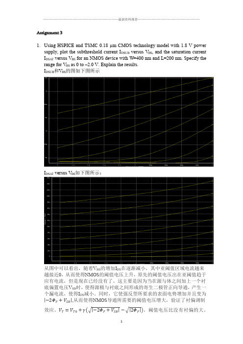
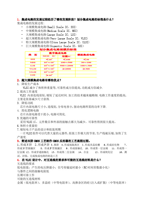
Assignment 3ing HSPICE and TSMC 0.18 µm CMOS technology model with 1.8 V powersupply, plot the subthreshold current I DSUB versus V BS, and the saturation currentI DSAT versus V BS for an NMOS device with W=400 nm and L=200 nm. Specify therange for V BS as 0 to –2.0 V. Explain the results.I DSUB和V BS的图如下图所示I DSAT versus V BS如下图所示:从图中可以看出,随着V BS的增加I DS在逐渐减小,其中亚阈值区域电流越来越接近0,从而使得NMOS的阈值电压上升,原先的阈值电压出在亚阈值趋于应有电流,但是现在已经没有了。
这主要是因为当在源与体之间加上一个衬底偏置电压V SB时,使得源极与衬底之间形成的寄生二极管正向导通,产生一个漏电流,使得I DS减小。
同时,它使强反型所要求的表面电势增加并且变为,从而使得NMOS导通所需要的阈值电压增大,验证了衬偏调制效应。
阈值电压比没有衬偏的大。
* SPICE INPUT FILE: problem.sp ID-VBS.param Supply=1.8 * Set value of Vdd.lib 'C:\synopsys\Hspice_A-2007.09\tsmc018\mm018.l' TT * Set 0.18um library .opt scale=0.1u * Set lambda*.model pch PMOS level=49 version=3.1*.model nch NMOS level=49 version=3.1mn Vdd gaten Gnd bn nch l=2 w=4 ad=20 pd=4 as=20 ps=4Vdd Vdd 0 'Supply'Vgsn gaten Gnd d cVbsn bn Gnd d c.dc Vbsn 0 -2 -0.05 Vgsn 0.6 1.8 0.2.print dc I1(mn).ending HSPICE and TSMC 0.18 um CMOS technology model with 1.8 V powersupply, plot log I DS versus V GS while varying V DS for an NMOS device withL=200 nm, W=800 nm and a PMOS with L=200 nm, W= 2 µm. Explain theresults.图中红线表示NMOS的I DS对V GS的曲线,从图中可以看出,随着V GS的增大I DS 的电流先为0,到后来逐渐增大,最后I DS对V GS的关系接近一个线性变化,且NMOS的导通电压约为0.43V,当V GS=0.43V的时候NMOS导通。
《超大规模集成电路设计》考试习题(含答案)完整版分析
1.集成电路的发展过程经历了哪些发展阶段?划分集成电路的标准是什么?集成电路的发展过程:•小规模集成电路(Small Scale IC,SSI)•中规模集成电路(Medium Scale IC,MSI)•大规模集成电路(Large Scale IC,LSI)•超大规模集成电路(Very Large Scale IC,VLSI)•特大规模集成电路(Ultra Large Scale IC,ULSI)•巨大规模集成电路(Gigantic Scale IC,GSI)划分集成电路规模的标准2.超大规模集成电路有哪些优点?1. 降低生产成本VLSI减少了体积和重量等,可靠性成万倍提高,功耗成万倍减少.2.提高工作速度VLSI内部连线很短,缩短了延迟时间.加工的技术越来越精细.电路工作速度的提高,主要是依靠减少尺寸获得.3. 降低功耗芯片内部电路尺寸小,连线短,分布电容小,驱动电路所需的功率下降.4. 简化逻辑电路芯片内部电路受干扰小,电路可简化.5.优越的可靠性采用VLSI后,元件数目和外部的接触点都大为减少,可靠性得到很大提高。
6.体积小重量轻7.缩短电子产品的设计和组装周期一片VLSI组件可以代替大量的元器件,组装工作极大的节省,生产线被压缩,加快了生产速度.3.简述双阱CMOS工艺制作CMOS反相器的工艺流程过程。
1、形成N阱2、形成P阱3、推阱4、形成场隔离区5、形成多晶硅栅6、形成硅化物7、形成N管源漏区8、形成P管源漏区9、形成接触孔10、形成第一层金属11、形成第一层金属12、形成穿通接触孔13、形成第二层金属14、合金15、形成钝化层16、测试、封装,完成集成电路的制造工艺4.在VLSI设计中,对互连线的要求和可能的互连线材料是什么?互连线的要求低电阻值:产生的电压降最小;信号传输延时最小(RC时间常数最小化)与器件之间的接触电阻低长期可靠工作可能的互连线材料金属(低电阻率),多晶硅(中等电阻率),高掺杂区的硅(注入或扩散)(中等电阻率)5.在进行版图设计时为什么要制定版图设计规则?—片集成电路上有成千上万个晶体管和电阻等元件以及大量的连线。
中科院数字集成系统设计(段成华)作业答案
Assignment 1:1.ITRS:International Technology Roadmap for Semiconductors 中文:国际半导体技术蓝图Gate-Equivalent:gate equivalent (GE) stands for a unit of measure which allows to specify manufacturing-technology-independent complexity of digital electronic circuitsTechnology Nodes:A technology node is defined as the ground rules of a process governed by the smallest feature printed in a repetitive arrayFeature size: The size of the elements on a chip, which is designated by the DRAM half pitch(动态随机存取存储器半间距). The smallest feature size is generally smaller than the feature size for a technology generation (technology node).Behavioral representation: representing a design as a Black Box and describe its outputs in term of its input and time行为表示:表示一种设计,这个设计只描述它们的输入和输出以及具体的时序结构。
Structural representation: A Black Box is represented as a set of components and connections结构表示:表示一种设计结构,其中的结构是由一系列的组件和连线构成Geometrical representation: it ignores what the design is supposed to do and binds its structure in space or to silicon.It entails the specification of all geometric patterns defining the physical layout of the chip, as well as their position几何表示:在这个结构中,不注意设计的目的是什么,只关心具体的几何实现,这种设计结构通过定义在芯片上的所有器件的物理布局甚至是具体位置来实现所有的几何设计。
中国科学院大学 段成华 VLSI 超大规模集成电路 期末复习笔记(1到10章)

MOS 管 耗尽区电荷以及宽度
阈值电压的定义,饱和区线性区等阶段的电流
阈值电压:强反型发生时
饱和区: 与 Vgs-Vt 平方成正比
线性区:
ID
n
(VGS
VT
)VDS
VDS 2
2
Vds 较小时忽略平方项,就是线性关系
沟调效应
增加 Vds 会使漏结的耗尽区变大,缩小了有效沟道长度。 影响为:Vds 会增大 ID
Vdd Vdd 0 'Supply' VgspVdd gatep dc='Supply' Vgsngaten Gnd dc='Supply'
.dc Vgsp0 'Supply' 'Supply/20' .dc Vgsn0 'Supply' 'Supply/20'
.print dc I1(mp) .print dc I1(mn)
* Set TSMC 0.18um library
*.model pch PMOS level=49 version = 3.1 *.model nch NMOS level=49 version = 3.1
.options list node post measout * Option List: Prints a list of netlist elements, node connections, and values for components, voltage and current sources, parameters, and more. * Option Node: Prints a node cross-reference table. * Option Post: Saves simulation results for viewing by an interactive waveform viewer. * Option Measout: Outputs .MEASURE statement values and sweep parameters into an ASCII file.
超大规模集成电路秋段成华老师第三次作业

超大规模集成电路2017年秋段成华老师第三次作业work Information Technology Company.2020YEARAssignment 3ing HSPICE and TSMC 0.18 µm CMOS technology model with 1.8 V powersupply, plot the subthreshold current I DSUB versus V BS, and the saturation currentI DSAT versus V BS for an NMOS device with W=400 nm and L=200 nm. Specify therange for V BS as 0 to –2.0 V. Explain the results.I DSUB和V BS的图如下图所示I DSAT versus V BS如下图所示:从图中可以看出,随着V BS的增加I DS在逐渐减小,其中亚阈值区域电流越来越接近0,从而使得NMOS的阈值电压上升,原先的阈值电压出在亚阈值趋于应有电流,但是现在已经没有了。
这主要是因为当在源与体之间加上一个衬底偏置电压V SB时,使得源极与衬底之间形成的寄生二极管正向导通,产生一个漏电流,使得I DS减小。
同时,它使强反型所要求的表面电势增加并且变为|−2ΦF+V SB|,从而使得NMOS导通所需要的阈值电压增大,验证了衬偏调制效应。
V T=V T0+γ(√|−2ΦF+V SB|−√|2ΦF|)。
阈值电压比没有衬偏的大。
* SPICE INPUT FILE: problem.sp ID-VBS.param Supply=1.8 * Set value of Vdd.lib 'C:\synopsys\Hspice_A-2007.09\tsmc018\mm018.l' TT * Set 0.18umlibrary.opt scale=0.1u * Set lambda*.model pch PMOS level=49 version=3.1*.model nch NMOS level=49 version=3.1mn Vdd gaten Gnd bn nch l=2 w=4 ad=20 pd=4 as=20 ps=4Vdd Vdd 0 'Supply'Vgsn gaten Gnd dcVbsn bn Gnd dc.dc Vbsn 0 -2 -0.05 Vgsn 0.6 1.8 0.2.print dc I1(mn).ending HSPICE and TSMC 0.18 um CMOS technology model with 1.8 V powersupply, plot log I DS versus V GS while varying V DS for an NMOS device withL=200 nm, W=800 nm and a PMOS with L=200 nm, W= 2 µm. Explain the results.图中红线表示NMOS的I DS对V GS的曲线,从图中可以看出,随着V GS的增大I DS的电流先为0,到后来逐渐增大,最后I DS对V GS的关系接近一个线性变化,且NMOS的导通电压约为0.43V,当V GS=0.43V的时候NMOS导通。
超大规模集成电路第四次作业2016秋_段成华
1. Shown below are buffer-chain designs.(1) Calculate the minimum delay of a chain of inverters for the overalleffective fan-out of 64/1.Solution :由题可知:64=F 根据经验6.3=opt f 为最合适的值,所以6.364===N N F f ,所以24.3=N ,但是级数必须为整数所以取3=N ,又因为1=γ,所以:15)641(3,464303=+⨯===p p t t f ,所以时最合适4=f 。
(2) Using HSPICE and TSMC 0.18 um CMOS technology model with1.8 V power supply, design a circuit simulation scheme to verify themwith their correspondent parameters of N, f, and t p .Solution:根据(1)中计算知道三级最合适,所以验证如下:A )、一级无负载测本征延时代码如下:.title buffer-chain 1.lib 'C:\synopsys\Hspice_D-2010.03-SP1\tsmc018\mm018.l' TT * set0.18um library.opt scale=0.1u * set lambda.options post=2 list.temp 27.global vddVdd vdd gnd 1.8vin vin 0 0.9 pulse 0 1.8 25n 5p 5p 49.99n 100n $频率为10MhzCl vout gnd 0f $Cg1=2.46fF,负载为CL=157.44fF.subckt inv in out wn=3.5 wp=10 t=7.5mn out in gnd gnd NCH l=2 w=wn ad='wn*t' pd='wn+2*t' as='wn*t' ps='wn+2*t'mp out in vdd vdd PCH l=2 w=wp ad='wp*t' pd='wp+2*t' as='wp*t' ps='wp+2*t'.endsX1 vin vout inv wn=3.5 wp=10 t=7.5.op.tran 5p 5n.meas tran voutmax max v(vout) from=5p to=5n.meas tran voutmin min v(vout) from=5p to=5n$一级.meas tran tphl1+trig v(vin)+val=0.9+rise=1+targ v(vout)+val='0.5*(voutmax-voutmin)+voutmin'+fall=1.meas tran tplh1+trig v(vin)+val=0.9+fall=1+targ v(vout)+val='0.5*(voutmax-voutmin)+voutmin'+rise=1.end1)一级无负载测得本征延时约为17ps;2)带上64倍Cg1大小的负载测得延时为750.35ps,是本征延时的44倍B)、三级带负载测延时代码如下:.title buffer-chain 3.lib 'C:\synopsys\Hspice_D-2010.03-SP1\tsmc018\mm018.l' TT * set 0.18um library.opt scale=0.1u * set lambda.options post=2 list.temp 27.global vdd.param fan=4Vdd vdd gnd 1.8vin vin 0 0.9 pulse 0 1.8 25n 5p 5p 49.99n 100nCl vout gnd 0f $Cg1=2.46fF,负载为CL=157.44fF.subckt inv in out wn=3.5 wp=10 t=7.5mn out in gnd gnd NCH l=2 w=wn ad='wn*t' pd='wn+2*t' as='wn*t' ps='wn+2*t'mp out in vdd vdd PCH l=2 w=wp ad='wp*t' pd='wp+2*t' as='wp*t' ps='wp+2*t'.endsX1 vin 2 inv wn=3.5 wp=10 t=7.5X2 2 3 inv wn='fan*3.5' wp='fan*10' t=5X3 3 vout inv wn='fan*fan*3.5' wp='fan*fan*10' t=5.op.tran 50p 500n.meas tran voutmax max v(vout) from=50p to=500n.meas tran voutmin min v(vout) from=50p to=500n$三级.meas tran tphl3+trig v(vin)+val=0.9+rise=1+targ v(vout)+val='0.5*(voutmax-voutmin)+voutmin'+fall=1.meas tran tplh3+trig v(vin)+val=0.9+fall=1+targ v(vout)+val='0.5*(voutmax-voutmin)+voutmin'+rise=11)带上64倍Cg1大小的负载测得延时为174.6ps ,是本征延时的10.27倍总结如下:经过调整参数近似时每一级的1=γ,所以经过手工计算得到一级带负载和三级带负载的延时比值为:2344.065151300==p p t t tp tp ,而仿真得到的结果为2327.035.7506.174=,所以符合手工计算的比值,同理其他级的延时代码也是如上的写法,经过仿真得到三级延时最小。
- 1、下载文档前请自行甄别文档内容的完整性,平台不提供额外的编辑、内容补充、找答案等附加服务。
- 2、"仅部分预览"的文档,不可在线预览部分如存在完整性等问题,可反馈申请退款(可完整预览的文档不适用该条件!)。
- 3、如文档侵犯您的权益,请联系客服反馈,我们会尽快为您处理(人工客服工作时间:9:00-18:30)。
Assignment 81.Access relevant reference books or technical data books and give accuratedefinitions for the following timing parameters:(1)design entity,(2)signal driver,(3)transaction,(4)event,(5)time queue,(6)delta delay,(7)simulation time,(8)simulation cycle,(9)inertial time,(10)transport time.(1)design entity: In VHDL a given logic circuit represented as a design entity. Adesign entity, in return , consists of two different types of description: the interface description and one or more architectural bodies. The interface description declares the entity and describes its inputs and outputs.(2)signal driver: If a process contains one or more signal assignment statementthat schedule future values for some signal X, the VHDL simulator creates a single value holder called a signal driver.(3)transaction:A pair consisting of a value and time. The value part represents afuture value of the driver; the time part represents the time at which the value part becomes the current value of driver.(4)event: It’s a kind of signal property and presents signal jump. Such asif(clk'event and clk='1).(5)time queue: It’s used to keep some signal transactions in the simulator. Timequeue entries are represented as a two-tuple of the form(SN,V), where SN is a signal name and V is the value the signal is scheduled to assume at the scheduled time. Each time queue entry is called a signal transaction.(6)delta delay: A period of time greater than 0, but less than any standard time unitno number of delta delay added together can cause simulation time to advance.(7)simulation time: The elapsed time in standard time units during simulation.(8)simulation cycle: Every time simulation time advances, a simulation cycleoccurs, which we now define more formally. The execution of a model consists of an initialization phase followed by the repetitive execution of processes in the process network. Each repetition is said to be a simulation cycle.(9)inertial time: Example: Z <= I after 10ns; The signal propagation will takeplace if and only if input I persists at a given level for 10ns-the amount of time specified in the after clause.(10)transport time: Z <= transport I after 10ns; All changes on I will propagate toZ, regardless of how long the value of I stays at the new level.2.Construct VHDL models for 74-139 dual 2-to-4-line decoders using threedescription types, i.e., behavioral, dataflow and structural descriptions. Synthesize and simulate these models respectively in the environment of Xilinx ISE with the ModelSim simulator integrated. When simulating these models, test vector(s) are required to stimulate the units under test (UUT). Reasonable test vectors are designed and created by your own as sources added to your VHDL project.Logic schematic of 74-139:Function table of one decoder of 74-139:(1-- Company:-- Engineer:-- Create Date: 21:14:09 12/02/2016-- Design Name:-- Module Name: deceoder_beh - Behavioral -- Project Name:-- Target Devices:-- Tool versions:-- Description:-- Dependencies:-- Revision:-- Revision 0.01 - File Created-- Additional Comments:library IEEE;use IEEE.STD_LOGIC_1164.ALL;use IEEE.STD_LOGIC_ARITH.ALL;use IEEE.STD_LOGIC_UNSIGNED.ALL;---- Uncomment the following library declaration if instantiating ---- any Xilinx primitives in this code.--library UNISIM;--use UNISIM.VComponents.all;entity deceoder_beh isPort ( G1,G2 : in std_logic;A : in std_logic_vector(1 downto 0);B : in std_logic_vector(1 downto 0);Y1 : out std_logic_vector(3 downto 0);Y2 : out std_logic_vector(3 downto 0));end deceoder_beh;architecture Behavioral of deceoder_beh isbeginde1: process (A, G1)beginif G1 = '1' theny1 <= "1111"; -- sequential statementelsecase A iswhen "00" => Y1 <= "1110";when "01" => Y1 <= "1101";when "10" => Y1 <= "1011";when "11" => Y1 <= "0111";when others => Y1 <= "1111";end case;end if;end process;de2: process (B, G2)beginif G2 = '1' thenY2 <= "1111"; -- sequential statementelsecase B iswhen "00" => Y2 <= "1110";when "01" => Y2 <= "1101";when "10" => Y2 <= "1011";when "11" => Y2 <= "0111";when others => Y2 <= "1111";end case;end if;end process;end Behavioral;TestBench代码如下:-- Company:-- Engineer:-- Create Date: 22:25:59 12/02/2016-- Design Name:-- Module Name: D:/ISE11.1_example/decoder/deconder_beh_tb.vhd-- Project Name: decoder-- Target Device:-- Tool versions:-- Description:-- VHDL Test Bench Created by ISE for module: deceoder_beh-- Dependencies:-- Revision:-- Revision 0.01 - File Created-- Additional Comments:-- Notes:-- This testbench has been automatically generated using types std_logic and -- std_logic_vector for the ports of the unit under test. Xilinx recommends-- that these types always be used for the top-level I/O of a design in order-- to guarantee that the testbench will bind correctly to the post-implementation -- simulation model.LIBRARY ieee;USE ieee.std_logic_1164.ALL;USE ieee.std_logic_unsigned.all;USE ieee.numeric_std.ALL;ENTITY deconder_beh_tb ISEND deconder_beh_tb;ARCHITECTURE behavior OF deconder_beh_tb IS-- Component Declaration for the Unit Under Test (UUT)COMPONENT deceoder_behPORT(G1 : IN std_logic;G2 : IN std_logic;A : IN std_logic_vector(1 downto 0);B : IN std_logic_vector(1 downto 0);Y1 : OUT std_logic_vector(3 downto 0);Y2 : OUT std_logic_vector(3 downto 0));END COMPONENT;--Inputssignal G1 : std_logic := '0';signal G2 : std_logic := '0';signal A : std_logic_vector(1 downto 0) := (others => '0');signal B : std_logic_vector(1 downto 0) := (others => '0');--Outputssignal Y1 : std_logic_vector(3 downto 0);signal Y2 : std_logic_vector(3 downto 0);BEGIN-- Instantiate the Unit Under Test (UUT)uut: deceoder_beh PORT MAP (G1 => G1,G2 => G2,A => A,B => B,Y1 => Y1,Y2 => Y2);-- Stimulus processstim_proc: processbegin-- insert stimulus hereG1 <='1';WAIT FOR 100 ns;G1 <='0';A <= "00";B <= "00";-- --------------------------------------- ------------- Current Time: 200nsWAIT FOR 100 ns;G1 <='0';A <= "01";B <= "01";-- --------------------------------------- ------------- Current Time: 300nsWAIT FOR 100 ns;G1 <='0';A <= "10";B <= "10";-- --------------------------------------- ------------- Current Time: 400nsWAIT FOR 100 ns;G1 <='0';a <= "11";b <= "11";WAIT FOR 100 ns;end process;END;测试波形如下:可以看到当G1=0和G2=0可以正常的译码,当G1=1和G2=1,则Y1和Y2都输出”1111”。