24c02中文官方资料手册pdf
24c02中文官方资料手册pdf

CAT24WC01/02/04/08/16 是 一 个 1K/2K/4K/8K/16K 位 串 行 CMOS E2PROM 内 部 含 有 128/256/512/1024/2048 个 8 位字节 CATALYST 公司的先进 CMOS 技术实质上减少了器件的功耗 CAT24WC01 有一个 8 字节页写缓冲器 CAT24WC02/04/08/16 有一个 16 字节页写缓冲器 该器件通过 I2C 总线接口进行操作 有一个专门的写保护功能
管脚描述
SCL 串行时钟 CAT24WC01/02/04/08/16 串行时钟输入管脚用于产生器件所有数据发送或接收的时钟 这是一个输 入管脚 SDA 串行数据/地址 CAT24WC01/02/04/08/16 双向串行数据/地址管脚用于器件所有数据的发送或接收 SDA 是一个开漏 输出管脚 可与其它开漏输出或集电极开路输出进行线或 wire-OR A0 A1 A2 器件地址输入端 这些输入脚用于多个器件级联时设置器件地址 当这些脚悬空时默认值为 0 24WC01 除外 当使用 24WC01 或 24WC02 时最大可级联 8 个器件 如果只有一个 24WC02 被总线寻址 这三个地 址输入脚 A0 A1 A2 可悬空或连接到 Vss 如果只有一个 24WC01 被总线寻址 这三个地址输入 脚 A0 A1 A2 必须连接到 Vss 当使用 24WC04 时最多可连接 4 个器件 该器件仅使用 A1 A2 地址管脚 A0 管脚未用 可以连 接到 Vss 或悬空 如果只有一个 24WC04 被总线寻址 A1 和 A2 地址管脚可悬空或连接到 Vss 当使用 24WC08 时最多可连接 2 个器件 且仅使用地址管脚 A2 A0 A1 管脚未用 可以连接到 Vss 或悬空 如果只有一个 24WC08 被总线寻址 A2 管脚可悬空或连接到 Vss 当使用 24WC16 时最多只可连接 1 个器件 所有地址管脚 A0 A1 A2 都未用 管脚可以连接到 Vss 或悬空 WP 写保护 如果 WP 管脚连接到 Vcc 所有的内容都被写保护 只能读 当 WP 管脚连接到 Vss 或悬空 允许 器件进行正常的读/写操作
24C02

© 1996 Microchip Technology Inc.PreliminaryDS21170A-page 1FEATURES•ISO Standard 7816 pad locations •Low power CMOS technology - 1 mA active current typical-10 µ A standby current typical at 5.5V•Organized as a single block of 128 bytes (128 x 8) or 256 bytes (256 x 8)•Two-wire serial interface bus, I 2 C ™compatible •100 kHz and 400 kHz compatibility•Self-timed write cycle (including auto-erase)•Page-write buffer for up to 8 bytes• 2 ms typical write cycle time for page-write •ESD protection > 4 kV•1,000,000 E/W cycles guaranteed •Data retention > 200 years•Available for extended temperature ranges DESCRIPTIONThe Microchip Technology Inc. 24C01SC and 24C02SC are 1K-bit and 2K-bit Electrically Erasable PROMs with bondpad positions optimized for smart card applications. The devices are organized as a sin-gle block of 128 x 8-bit or 256 x 8-bit memory with a two-wire serial interface. The 24C01SC and 24C02SC also have page-write capability for up to 8 bytes of data.-Commercial (C):0 ° C to +70 ° CDIE LAYOUTBLOCK DIAGRAMSDA DCV CCSCLV SSHV GENERATOREEPROM ARRAY PAGE LATCHESYDECXDECSENSE AMP R/W CONTROLMEMORY CONTROL LOGICI/O CONTROL LOGIC SDA SCLV CC V SS1K/2K 5.0V I 2C Serial EEPROMs for Smart Cards24C01SC/02SCI 2C is a trademark of Philips Corporation.This document was created with FrameMaker 40424C01SC/02SCDS21170A-page 2 ©1996 Microchip Technology Inc.1.0ELECTRICAL CHARACTERISTICSMaximum Ratings*V CC ..............................................................7.0VAll inputs and outputs w.r.t. V SS ......-0.6V to VCC +1.0V Storage temperature..........................-65˚C to +150˚C Ambient temp. with power applied.......-65˚C to +125˚C ESD protection on all pads ....................................≥ 4 kV*Notice: Stresses above those listed under “Maximum ratings”may cause permanent damage to the device. This is a stress rat-ing only and functional operation of the device at those or any other conditions above those indicated in the operational listings of this specification is not implied. Exposure to maximum rating conditions for extended periods may affect device reliability.TABLE 1-1:PAD FUNCTION TABLEName Function V SS SDA SCL V CC DCGroundSerial Address/Data I/O Serial Clock+4.5V to 5.5V Power Supply Don’t connectTABLE 1-2:DC CHARACTERISTICSFIGURE 1-1:BUS TIMING START/STOPV CC = +4.5V to +5.5VCommercial (C):Tamb = 0˚C to +70˚C ParameterSymbol Min.Max.Units ConditionsSCL and SDA pads:High level input voltageV IH .7 V CC ——Low level input voltageV IL —.3 V CC V Hysteresis of Schmidt trigger inputs V HYS .05 V CC—V (Note)Low level output voltage V OL —.40V I OL = 3.0 mA, V CC = 4.5V Input leakage current (SCL)I LI -1010 µ A V IN = .1V to 5.5V Output leakage current (SDA)I LO -1010 µ A V OUT = .1V to 5.5V Pin capacitance (all inputs/outputs)C IN , C OUT —10pF V CC = 5.0V (Note 1)Tamb = 25˚C, F CLK = 1 MHz Operating currentI CC Write —3mA V CC = 5.5VI CC Read—1mA Vcc = 5.5V , SCL = 400 KHz Standby current I CCS—100µ AV CC = 5.5V , SDA = SCL = VCCNote:This parameter is periodically sampled and not 100% tested.SCLSDAT SU :STAT HD :STASTART STOPV HYST SU :STO© 1996 Microchip Technology Inc.Preliminary24C01SC/02SCTABLE 1-3:AC CHARACTERISTICSFIGURE 1-2:BUS TIMING DATAParameterSymbol Min.Max.Units RemarksClock frequency F CLK —400kHz Clock high time T HIGH 600—ns Clock low time T LOW 1300—ns SDA and SCL rise time T R —300ns (Note 1)SDA and SCL fall time T F —300ns (Note 1)START condition hold time T HD : STA 600—ns After this period the first clock pulse is generated START condition setup time T SU : STA 600—ns Only relevant for repeated START condition Data input hold time T HD : DAT 0—ns (Note 2)Data input setup time T SU : DAT 100—ns STOP condition setup time T SU : STO 600—ns Output valid from clock T AA —900ns (Note 2)Bus free timeT BUF1300—nsTime the bus must be free before a new transmission can startOutput fall time from V IH minimum to V IL maximum TOF 20 +0.1 CB 250ns (Note 1), CB ≤ 100 pF Input filter spike suppression (SDA and SCL pins)T SP —50ns (Note 3)Write cycle time T WR —10ms Byte or Page modeEndurance—106—cycles25 ° C, Vcc = 5V , Block Mode (Note 4)Note 1:Not 100% tested. CB = total capacitance of one bus line in pF .2:As a transmitter, the device must provide an internal minimum delay time to bridge the undefined region(minimum 300 ns) of the falling edge of SCL to avoid unintended generation of START or STOP conditions.3:The combined T SP and VHYSspecifications are due to new Schmitt trigger inputs which provide improvednoise spike suppression. This eliminates the need for a TI specification for standard operation.4:This parameter is not tested but guaranteed by characterization. For endurance estimates in a specific appli-cation, please consult the Total Endurance Model which can be obtained on our BBS or website.SCLSDA INSDA OUTT HD :STAT SU :STAT FT HIGHT RT SU :STOT SU :DATT HD :DATT BUFT AA T HD :STAT AAT SPT LOW24C01SC/02SCDS21170A-page 4 ©1996 Microchip Technology Inc.2.0FUNCTIONAL DESCRIPTIONThe 24C01SC/02SC supports a bi-directional two-wire bus and data transmission protocol. A device that sends data onto the bus is defined as transmitter, and a device receiving data as receiver. The bus has to be controlled by a master device which generates the serial clock (SCL), controls the bus access, and gener-ates the START and STOP conditions, while the 24C01SC/02SC works as slave. Both master and slave can operate as transmitter or receiver, but the master device determines which mode is activated.3.0BUS CHARACTERISTICSThe following bus protocol has been defined:•Data transfer may be initiated only when the bus is not busy.•During data transfer, the data line must remain stable whenever the clock line is HIGH. Changes in the data line while the clock line is HIGH will be interpreted as a START or STOP condition.Accordingly, the following bus conditions have been defined (Figure 3-1).3.1Bus not Busy (A)Both data and clock lines remain HIGH.3.2Start Data Transfer (B)A HIGH to LOW transition of the SDA line while the clock (SCL) is HIGH determines a START condition. All commands must be preceded by a START condition.3.3Stop Data Transfer (C)A LOW to HIGH transition of the SDA line while the clock (SCL) is HIGH determines a STOP condition. All operations must be ended with a STOP condition.3.4Data Valid (D)The state of the data line represents valid data when,after a START condition, the data line is stable for the duration of the HIGH period of the clock signal.The data on the line must be changed during the LOW period of the clock signal. There is one clock pulse per bit of data.Each data transfer is initiated with a START condition and terminated with a STOP condition. The number of the data bytes transferred between the START and STOP conditions is determined by the master device and is theoretically unlimited, although only the last 16will be stored when doing a write operation. When an overwrite does occur, it will replace data in a first in first out fashion.3.5AcknowledgeEach receiving device, when addressed, is obliged to generate an acknowledge after the reception of each byte. The master device must generate an extra clock pulse which is associated with this acknowledge bit.The device that acknowledges has to pull down the SDA line during the acknowledge clock pulse in such a way that the SDA line is stable LOW during the HIGH period of the acknowledge related clock pulse. Of course, setup and hold times must be taken into account. A master must signal an end of data to the slave by not generating an acknowledge bit on the last byte that has been clocked out of the slave. In this case,the slave must leave the data line HIGH to enable the master to generate the STOP condition.Note:The 24C01SC/02SC does not generate any acknowledge bits if an internal pro-gramming cycle is in progress.FIGURE 3-1:DATA TRANSFER SEQUENCE ON THE SERIAL BUSSCLSDA(A )(B)(D)(D)(C)(A )START CONDITIONADDRESS OR ACKNOWLEDGEVALID DATA ALLOWED TO CHANGESTOP CONDITION© 1996 Microchip Technology Inc.PreliminaryDS21170A-page 524C01SC/02SC4.0BUS CHARACTERISTICS4.1Slave AddressAfter generating a START condition, the bus master transmits the slave address consisting of a 4-bit device code (1010) for the 24C01SC/02SC, followed by three don't care bits.The eighth bit of slave address determines if the master device wants to read or write to the 24C01SC/02SC (Figure 4-1).The 24C01SC/02SC monitors the bus for its corre-sponding slave address all the time. It generates an acknowledge bit if the slave address was true, and it is not in a programming mode.FIGURE 4-1:CONTROL BYTE ALLOCATIONOperation Control Code Chip Select R/W Read Write10101010XX XXX10X = Don’t careR/W A1010X X XREAD/WRITESTARTSLAVE ADDRESS 5.0WRITE OPERATION5.1Byte WriteFollowing the start signal from the master, the device code (4 bits), the don't care bits (3 bits), and the R/W bit, which is a logic low, is placed onto the bus by the master transmitter. This indicates to the addressed slave receiver that a byte with a word address will follow after it has generated an acknowledge bit during the ninth clock cycle. Therefore, the next byte transmitted by the master is the word address and will be written into the address pointer of the 24C01SC/02SC. After receiving another acknowledge signal from the 24C01SC/02SC, the master device will transmit the data word to be written into the addressed memory location. The 24C01SC/02SC acknowledges again and the master generates a stop condition. This initiates the internal write cycle, and during this time the 24C01SC/02SC will not generate acknowledge signals (Figure 5-1).5.2Page WriteThe write control byte, word address, and the first data byte are transmitted to the 24C01SC/02SC in the same way as in a byte write. But instead of generating a stop condition, the master transmits up to eight data bytes to the 24C01SC/02SC, which are temporarily stored in the on-chip page buffer and will be written into the memory after the master has transmitted a stop condi-tion. After the receipt of each word, the three lower order address pointer bits are internally incremented by one. The higher order five bits of the word address remains constant. If the master should transmit more than eight words prior to generating the stop condition,the address counter will roll over and the previously received data will be overwritten. As with the byte write operation, once the stop condition is received an inter-nal write cycle will begin (Figure 5-2).FIGURE 5-1:BYTE WRITEFIGURE 5-2:PAGE WRITESPS T A R TS T O PBUS ACTIVITY MASTERSDA LINEBUS ACTIVITYA C KA C KA C KCONTROL BYTEWORD ADDRESSDATASPBUS ACTIVITY MASTERSDA LINEBUS ACTIVITYS T A R TS T O PCONTROL BYTEWORD ADDRESS (n)DATA nDATAn + 7DATAn + 1A C KA C KA C KA C KA C K24C01SC/02SCDS21170A-page 6Preliminary© 1996 Microchip Technology Inc.6.0ACKNOWLEDGE POLLINGSince the device will not acknowledge during a write cycle, this can be used to determine when the cycle is complete (this feature can be used to maximize bus throughput). Once the stop condition for a write com-mand has been issued from the master, the device ini-tiates the internally timed write cycle. ACK polling can be initiated immediately. This involves the master send-ing a start condition followed by the control byte for a write command (R/W = 0). If the device is still busy with the write cycle, then NO ACK will be returned. If the cycle is complete, then the device will return the ACK,and the master can then proceed with the next read or write command. See Figure 6-1 for flow diagram.FIGURE 6-1:ACKNOWLEDGE POLLING FLOWSendWrite CommandSend Stop Condition to Initiate Write CycleSend StartSend Control Byte with R/W = 0Did Device Acknowledge (ACK = 0)?Next OperationNOYES7.0READ OPERATIONRead operations are initiated in the same way as write operations with the exception that the R/W bit of the slave address is set to one. There are three basic types of read operations: current address read, random read,and sequential read.7.1Current Address ReadThe 24C01SC/02SC contains an address counter that maintains the address of the last word accessed, inter-nally incremented by one. Therefore, if the previous access (either a read or write operation) was to address n, the next current address read operation would access data from address n + 1. Upon receipt of the slave address with R/W bit set to one, the 24C01SC/02SC issues an acknowledge and transmits the 8-bit data word. The master will not acknowledge the transfer but does generate a stop condition and the 24C01SC/02SC discontinues transmission (Figure 8-2).7.2Random ReadRandom read operations allow the master to access any memory location in a random manner. To perform this type of read operation, first the word address must be set. This is done by sending the word address to the 24C01SC/02SC as part of a write operation. After the word address is sent, the master generates a start con-dition following the acknowledge. This terminates the write operation, but not before the internal address pointer is set. Then, the master issues the control byte again but with the R/W bit set to a one. The 24C01SC/02SC will then issue an acknowledge and transmits the 8-bit data word. The master will not acknowledge the transfer but does generate a stop con-dition and the 24C01SC/02SC discontinues transmis-sion (Figure 8-3).7.3Sequential ReadSequential reads are initiated in the same way as a ran-dom read except that after the 24C01SC/02SC trans-mits the first data byte, the master issues an acknowledge as opposed to a stop condition in a ran-dom read. This directs the 24C01SC/02SC to transmit the next sequentially addressed 8-bit word (Figure 9-1).To provide sequential reads the 24C01SC/02SC con-tains an internal address pointer which is incremented by one at the completion of each operation. This address pointer allows the entire memory contents to be serially read during one operation.© 1996 Microchip Technology Inc.PreliminaryDS21170A-page 724C01SC/02SC7.4Noise ProtectionThe 24C01SC/02SC employs a V CC threshold detector circuit which disables the internal erase/write logic if the V CC is below 1.5 volts at nominal conditions.The SCL and SDA inputs have Schmitt trigger and filter circuits which suppress noise spikes to assure proper device operation even on a noisy bus.FIGURE 7-1:CURRENT ADDRESS READFIGURE 7-2:RANDOM READFIGURE 7-3:SEQUENTIAL READSPBUS ACTIVITY MASTERSDA LINEBUS ACTIVITYS T A R TCONTROL BYTEDATA nA C KN OA C KS T O PSPSBUS ACTIVITY MASTER SDA LINEBUS ACTIVITYS TA RT S T O PCONTROL BYTEWORD ADDRESS (n)DATA nA C KA C KN OA C KCONTROL BYTEA C KS T A R TPBUS ACTIVITYS T O PCONTROL BYTEDATA nA C KN OA C KA C KA C KA C KDATA n + 1DATA n + 2DATA n + XBUS ACTIVITY MASTER24C01SC/02SCDS21170A-page 8Preliminary© 1996 Microchip Technology Inc.8.0PAD DESCRIPTIONS8.1SDA Serial Address/Data Input/OutputThis is a bi-directional pad used to transfer addresses and data into and data out of the device. It is an open drain terminal, therefore the SDA bus requires a pull-up resistor to V CC (typical 10K Ω for 100 kHz, 1K Ω for 400kHz).For normal data transfer SDA is allowed to change only during SCL low. Changes during SCL high are reserved for indicating the START and STOP conditions.8.2SCL Serial ClockThis input is used to synchronize the data transfer from and to the device.8.3DC Don’t ConnectThis pad is used for test purposes and should not be bonded out. It will be pulled to V SS through an internal resistor.9.0DIE CHARACTERISTICSFigure 9-1 shows the die layout of the 24C01SC/02SC,including bondpad positions. Table 9-1 shows the actual coordinates of the bondpad midpoints with respect to the center of the die.FIGURE 9-1:DIE LAYOUTTABLE 9-1:BONDPAD COORDINATESPad NamePad Midpoint,X dir.Pad Midpoint,Y dir.V SS-495.000749.130SDA -605.875-271.875SCL 479.875-746.625V CC 605.875-261.375Note 1:Dimensions are in microns.2:Center of die is at the 0,0 point.DIPSDA DCV CCSCLV SS24C01SC/02SC NOTES:© 1996 Microchip Technology Inc.Preliminary DS21170A-page 924C01SC/02SCNOTES:DS21170A-page 10Preliminary© 1996 Microchip Technology Inc.24C01SC/02SC24C01SC/02SC Product Identification SystemTo order or to obtain information (e.g., on pricing or delivery), please use the listed part numbers, and refer to the factory or the listed sales offices.24C01SC/02SC—/S XXDie Thickness Blank=11 mils08=8 milsOther die thicknesses available, pleaseconsult factory.Package:S=Die in Wafer PakW=WaferWF=Sawed Wafer on FrameTemperature Blank=0°C to +70°CRange:Device:24C01SC1K 12C ISO Smart Card die24C02SC2K 12C ISO Smart Card die© 1996 Microchip Technology Inc.Preliminary DS21170A-page 11DS21170A-page 12Preliminary© 1996 Microchip Technology Inc.WORLDWIDE S ALES & S ERVICEAMERICAS (continued)New YorkMicrochip T echnology Inc.150 Motor Parkway, Suite 416Hauppauge, NY 11788T el: 516 273-5305 Fax: 516 273-5335San JoseMicrochip T echnology Inc.2107 North First Street, Suite 590San Jose, CA 95131T el: 408 436-7950 Fax: 408 436-7955TorontoMicrochip T echnology Inc.5925 Airport Road, Suite 200Mississauga, Ontario L4V 1W1, Canada T el: 905 405-6279Fax: 905 405-6253ASIA/PACIFICHong KongMicrochip T echnology Rm 3801B, T ower T wo Metroplaza,223 Hing Fong Road,Kwai Fong, N.T ., Hong KongT el: 852 2 401 1200 Fax: 852 2 401 3431KoreaMicrochip T echnology168-1, Y oungbo Bldg. 3 Floor Samsung-Dong, Kangnam-Ku,Seoul, KoreaT el: 82 2 554 7200 Fax: 82 2 558 5934SingaporeMicrochip T echnology 200 Middle Road #10-03 Prime Centre Singapore 188980T el: 65 334 8870 Fax: 65 334 8850TaiwanMicrochip T echnology 10F-1C 207T ung Hua North Road T aipei, T aiwan, ROCT el: 886 2 717 7175 Fax: 886 2 545 0139EUROPEUnited KingdomArizona Microchip T echnology Ltd.Unit 6, The CourtyardMeadow Bank, Furlong RoadBourne End, Buckinghamshire SL8 5AJT el: 44 1 628 850303 Fax: 44 1 628 850178FranceArizona Microchip T echnology SARL Zone Industrielle de la Bonde 2 Rue du Buisson aux Fraises 91300 Massy - FranceT el: 33 1 69 53 63 20 Fax: 33 1 69 30 90 79GermanyArizona Microchip T echnology GmbH Gustav-Heinemann-Ring 125D-81739 Muenchen, GermanyT el: 49 89 627 144 0 Fax: 49 89 627 144 44ItalyArizona Microchip T echnology SRL Centro Direzionale ColleoniPalazzo T aurus 1 V . Le Colleoni 120041, Agrate Brianza, Milan ItalyT el: 39 39 689 9939 Fax: 39 39 689 9883JAPANMicrochip T echnology Intl. Inc.Benex S-1 6F3-18-20, Shin Y okohama Kohoku-Ku, Y okohama Kanagawa 222 JapanT el: 81 45 471 6166 Fax: 81 45 471 61225/10/96AMERICASCorporate OfficeMicrochip T echnology Inc.2355 West Chandler Blvd.Chandler, AZ 85224-6199T el: 602 786-7200 Fax: 602 786-7277Technical Support: 602 786-7627Web: /AtlantaMicrochip T echnology Inc.500 Sugar Mill Road, Suite 200B Atlanta, GA 30350T el: 770 640-0034Fax: 770 640-0307BostonMicrochip T echnology Inc.5 Mount Royal Avenue Marlborough, MA 01752T el: 508 480-9990Fax: 508 480-8575ChicagoMicrochip T echnology Inc.333 Pierce Road, Suite 180Itasca, IL 60143T el: 708 285-0071 Fax: 708 285-0075DallasMicrochip T echnology Inc.14651 Dallas Parkway, Suite 816Dallas, TX 75240-8809T el: 214 991-7177 Fax: 214 991-8588DaytonMicrochip T echnology Inc.Suite 150T wo Prestige PlaceMiamisburg, OH 45342T el: 513 291-1654 Fax: 513 291-9175Los AngelesMicrochip T echnology Inc.18201 Von Karman, Suite 1090Irvine, CA 92715T el: 714 263-1888 Fax: 714 263-1338Information contained in this publication regarding device applications and the like is intended through suggestion only and may be superseded by updates. No repre-sentation or warranty is given and no liability is assumed by Microchip Technology Incorporated with respect to the accuracy or use of such information, or infringement of patents or other intellectual property rights arising from such use or otherwise. Use of Microchip’s products as critical components in life support systems is not autho-rized except with express written approval by Microchip. No licenses are conveyed, implicitly or otherwise, under any intellectual property rights. The Microchip logo and name are registered trademarks of Microchip Technology Inc. All rights reserved. All other trademarks mentioned herein are the property of their respective companies.All rights reserved. © 1996, Microchip Technology Incorporated, USA. 5/96。
at24c02中文资料_数据手册_参数

FM24C02中文资料
元器件交易网
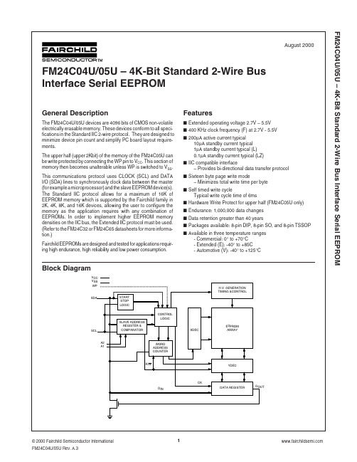
FM24C04U/05U – 4K-Bit Standard 2-Wire Bus Interface Serial EEPROM
Ordering Information FM 24 C XX U F LZ E XXX
Operating Conditions
Ambient Operating Temperature FM24C04U/05U FM24C04UE/05UE FM24C04UV/05UV Positive Power Supply FM24C04U/05U FM24C04UL/05UL FM24C04ULZ/05ULZ 0°C to +70°C -40°C to +85°C -40°C to +125°C 4.5V to 5.5V 2.7V to 5.5V 2.7V to 5.5V
FM24C04U/05U – 4K-Bit Standard 2-Wire Bus Interface Serial EEPROM
Product Specifications Absolute Maximum Ratings
Ambient Storage Temperature All Input or Output Voltages with Respect to Ground Lead Temperature (Soldering, 10 seconds) ESD Rating –65°C to +150°C –0.3V to 6.5V +300°C 2000V min.
元器件交易网
FM24C04U/05U – 4K-Bit Standard 2-Wire Bus Interface Serial EEPROM
24C02资料 (2)
一、EPROM与EEPROM:EPROM(Erasable Programmable Read Only Memory),中文含意为“可擦除可编程只读存储器”。
它是一种可重写的存储器芯片,并且其内容在掉电的时候也不会丢失;换句话说,它是非易失性的。
它通过EPROM编程器进行编程,EPROM编程器能够提供比正常工作电压更高的电压对EPROM编程。
一旦经过编程,EPROM只有在强紫外线的照射下才能够进行擦除。
为了进行擦除,EPROM的陶瓷封装上具有一个小的石英窗口,这个石英窗口一般情况下使用不透明的粘带覆盖,当擦除时将这个粘带揭掉,然后放置在强紫外线下大约20分钟。
主要IC有27XX系列和27CXX系列。
EEPROM(electrically erasable, programmable, read-only )是一种电可擦除可编程只读存储器,并且其内容在掉电的时候也不会丢失。
在平常情况下,EEPROM与EPROM一样是只读的,需要写入时,在指定的引脚加上一个高电压即可写入或擦除,而且其擦除的速度极快!通常EEPROM芯片又分为串行EEPROM和并行EEPROM两种,串行EEPROM在读写时数据的输入/输出是通过2线、3线、4线或SPI 总线等接口方式进行的,而并行EEPROM的数据输入/输出则是通过并行总线进行的。
主要IC有28XX系列。
二、24c02芯片硬件介绍:1、引脚说明:A0,A1,A2——地址输入引脚,走位硬件寻址的依据,同种芯片可同时连接8片(2^3);Vcc,Gnd——电源,接地引脚,1.8-5.5vWp——写保护,当Wp接地时,允许对器件的正常读写操作;当Wp接高电平时,写保护,只能进行读操作。
SDA——串行地址/数据输入/输出端口,双向传输,漏极开路,需外接上拉电阻到Vcc(典型阻值为10k)。
SCL——串行时钟输入,高低电平不同状态与SDA配合,执行不同的命令。
2、存储结构:24c02的容量是2k,256字节。
24C02C-EP中文资料

•Single supply with operation from 4.5 to 5.5V •Low power CMOS technology - 1 mA active current typical-10 µ A standby current typical at 5.5V•Organized as a single block of 256 bytes (256 x 8)•Hardware write protection for upper half of array •2-wire serial interface bus, I 2 C compatible •100 kHz and 400 kHz compatibility •Page-write buffer for up to 16 bytes•Self-timed write cycle (including auto-erase)•Fast 1 mS write cycle time for byte or page mode •Address lines allow up to eight devices on bus •1,000,000 erase/write cycles guaranteed •ESD protection > 4,000V •Data retention > 200 years•8-pin PDIP , SOIC or TSSOP packages •Available for extended temperature ranges DESCRIPTIONThe Microchip T echnology Inc. 24C02C is a 2K bit Serial Electrically Erasable PROM with a voltage range of 4.5V to 5.5V . The device is organized as a single block of 256 x 8-bit memory with a 2-wire serial inter-face. Low current design permits operation with typical standby and active currents of only 10 µ A and 1 mA respectively. The device has a page-write capability for up to 16 bytes of data and has fast write cycle times of only 1 mS for both byte and page writes. Functional address lines allow the connection of up to eight 24C02C devices on the same bus for up to 16K bits of contiguous EEPROM memory. The device is available in the standard 8-pin PDIP , 8-pin SOIC (150 mil), and TSSOP packages.-Commercial (C):0 ° C to +70 ° C -Industrial (I): -40 ° C to +85 ° C -Automotive (E): -40 ° C to +125 °C元器件交易网24C02C1.0ELECTRICALCHARACTERISTICS1.1Maximum Ratings*V CC ........................................................................7.0V All inputs and outputs w.r.t. V SS ......-0.6V to V CC +1.0V Storage temperature...........................-65˚C to +150˚C Ambient temp. with power applied.......-65˚C to +125˚C Soldering temperature of leads (10 seconds)...+300˚C ESD protection on all pins ......................................≥ 4 kV*Notice:Stresses above those listed under “Maximum ratings” may cause permanent damage to the device. This is a stress rating only and functional operation of the device at those or any other conditions above those indicated in the operational listings of this specification is not implied. Exposure to maximum rating conditions for extended peri-ods may affect device reliability.TABLE 1-1:PIN FUNCTION TABLEName Function V SS SDA SCL VCC A0, A1, A2WPGround Serial Data Serial Clock+4.5V to 5.5V Power Supply Chip SelectsHardware Write ProtectTABLE 1-2:DC CHARACTERISTICSAll parameters apply across the speci-fied operating ranges unless otherwise noted.VCC = +4.5V to +5.5V Commercial (C):T amb = 0 ° C to +70 ° C Industrial (I):Tamb = -40 ° C to +85 ° C Automotive (E):T amb = -40 ° C to +125 ° C ParameterSymbol Min.Max.Units ConditionsSCL and SDA pins:High level input voltageV IH 0.7 V CC—V Low level input voltageV IL —0.3 V CCV Hysteresis of Schmitt trigger inputs V HYS 0.05 V CC—V (Note)Low level output voltage V OL —0.40V I OL = 3.0 mA, Vcc = 4.5V Input leakage current ILI -1010 µ A V IN = 0.1V to 5.5V , WP = Vss Output leakage currentILO -1010 µ A V OUT = 0.1V to 5.5V Pin capacitance (all inputs/outputs)C IN , C OUT —10pF VCC = 5.0V (Note)T amb = 25 ° C, f = 1 MHz Operating current I CC Read —1mA V CC = 5.5V , SCL = 400 kHz I CC Write —3mA V CC = 5.5VStandby currentICCS—50µ AV CC = 5.5V , SDA = SCL = VCCNote: This parameter is periodically sampled and not 100% tested.元器件交易网24C02CTABLE 1-3:AC CHARACTERISTICSAll parameters apply across the specified oper-ating ranges unless otherwise noted.Vcc = 4.5V to 5.5V Commercial (C):Tamb = 0 ° C to +70 ° C Industrial (I):T amb = -40 ° C to +85 ° C Automotive (E):Tamb = -40 ° C to +125 ° C ParameterSymbol Tamb > +85 ° C -40 ° C ≤ Tamb ≤+85 ° CUnits RemarksMin.Max.Min.Max. Clock frequency F CLK —100—400kHz Clock high time T HIGH 4000—600—ns Clock low timeT LOW 4700—1300—ns SDA and SCL rise time T R —1000—300ns (Note 1)SDA and SCL fall time T F —300—300ns (Note 1)START condition hold time T HD : STA 4000—600—ns After this period the first clock pulse is generated START condition setup time T SU : STA 4700—600—ns Only relevant for repeated ST ART condition Data input hold time T HD : DAT 0—0—ns (Note 2)Data input setup timeT SU : DAT 250—100—ns STOP condition setup time T SU : STO 4000—600—ns Output valid from clock T AA —3500—900ns (Note 2)Bus free timeT BUF4700—1300—nsTime the bus must be free before a new transmission can startOutput fall time from V IH minimum to V IL maximum T OF —25020 + 0.1 C B250ns (Note 1), C B ≤ 100 pF Input filter spike suppression (SDA and SCL pins)T SP —50—50ns(Note 3)Write cycle time TWR— 1.5—1ms Byte or Page modeEndurance1M—1M—cycles 25 ° C, V CC = 5.0V , BlockMode (Note 4)Note 1: Not 100% tested. CB = total capacitance of one bus line in pF .2: As a transmitter, the device must provide an internal minimum delay time to bridge the undefined region (minimum 300 ns) of the falling edge of SCL to avoid unintended generation of ST ART or STOP conditions. 3:The combined T SP and V HYS specifications are due to Schmitt trigger inputs which provide improved noise spike suppression. This eliminates the need for a TI specification for standard operation.4:This parameter is not tested but guaranteed by characterization. For endurance estimates in a specific appli-cation, please consult the T otal Endurance Model which can be obtained on our BBS or website.元器件交易网24C02C2.0PIN DESCRIPTIONS2.1SDA Serial DataThis is a bi-directional pin used to transfer addresses and data into and data out of the device. It is an open drain terminal, therefore the SDA bus requires a pull-up resistor to V CC (typical 10 k Ω for 100 kHz, 2 k Ω for 400 kHz).For normal data transfer SDA is allowed to change only during SCL low. Changes during SCL high are reserved for indicating the ST ART and STOP conditions.2.2SCL Serial ClockThis input is used to synchronize the data transfer from and to the device.2.3A0, A1, A2The levels on these inputs are compared with the cor-responding bits in the slave address. The chip is selected if the compare is true.Up to eight 24C02C devices may be connected to the same bus by using different chip select bit combina-tions. These inputs must be connected to either V CC or V SS .2.4WPThis is the hardware write protect pin. It must be tied to V CC or V SS . If tied to Vcc, the hardware write protection is enabled. If the WP pin is tied to Vss the hardware write protection is disabled.2.5Noise ProtectionThe 24C02C employs a V CC threshold detector circuit which disables the internal erase/write logic if the V CC is below 3.8 volts at nominal conditions.The SCL and SDA inputs have Schmitt trigger and filter circuits which suppress noise spikes to assure proper device operation even on a noisy bus.3.0FUNCTIONAL DESCRIPTIONThe 24C02C supports a bi-directional 2-wire bus and data transmission protocol. A device that sends data onto the bus is defined as transmitter, and a device receiving data as receiver. The bus has to be controlled by a master device which generates the serial clock (SCL), controls the bus access, and generates the ST ART and STOP conditions, while the 24C02C works as slave. Both master and slave can operate as trans-mitter or receiver but the master device determines which mode is activated.元器件交易网24C02C4.0BUS CHARACTERISTICSThe following bus protocol has been defined:•Data transfer may be initiated only when the bus is not busy.•During data transfer, the data line must remain stable whenever the clock line is HIGH. Changes in the data line while the clock line is HIGH will be interpreted as a ST ART or STOP condition.Accordingly, the following bus conditions have been defined (Figure 4-1).4.1Bus not Busy (A)Both data and clock lines remain HIGH.4.2Start Data Transfer (B)A HIGH to LOW transition of the SDA line while the clock (SCL) is HIGH determines a START condition. All commands must be preceded by a ST ART condition.4.3Stop Data Transfer (C)A LOW to HIGH transition of the SDA line while the clock (SCL) is HIGH determines a STOP condition. All operations must be ended with a STOP condition.4.4Data Valid (D)The state of the data line represents valid data when,after a ST ART condition, the data line is stable for the duration of the HIGH period of the clock signal.The data on the line must be changed during the LOW period of the clock signal. There is one bit of data per clock pulse.Each data transfer is initiated with a START condition and terminated with a STOP condition. The number of the data bytes transferred between the ST ART and STOP conditions is determined by the master device and is theoretically unlimited, although only the last six-teen will be stored when doing a write operation. When an overwrite does occur it will replace data in a first in first out fashion.4.5AcknowledgeEach receiving device, when addressed, is required to generate an acknowledge after the reception of each byte. The master device must generate an extra clock pulse which is associated with this acknowledge bit.The device that acknowledges has to pull down the SDA line during the acknowledge clock pulse in such a way that the SDA line is stable LOW during the HIGH period of the acknowledge related clock pulse. Of course, setup and hold times must be taken into account. A master must signal an end of data to the slave by not generating an acknowledge bit on the last byte that has been clocked out of the slave. In this case,the slave must leave the data line HIGH to enable the master to generate the STOP condition (Figure 4-2).元器件交易网24C02C5.0DEVICE ADDRESSINGA control byte is the first byte received following the start condition from the master device (Figure 5-1). The control byte consists of a four bit control code; for the 24C02C this is set as 1010 binary for read and write operations. The next three bits of the control byte are the chip select bits (A2, A1, A0). The chip select bits allow the use of up to eight 24C02C devices on the same bus and are used to select which device is accessed. The chip select bits in the control byte must correspond to the logic levels on the corresponding A2,A1, and A0 pins for the device to respond. These bits are in effect the three most significant bits of the word address.The last bit of the control byte defines the operation to be performed. When set to a one a read operation is selected, and when set to a zero a write operation is selected. Following the start condition, the 24C02C monitors the SDA bus checking the control byte being transmitted. Upon receiving a 1010 code and appropri-ate chip select bits, the slave device outputs an acknowledge signal on the SDA line. Depending on the state of the R/W bit, the 24C02C will select a read or write operation.5.1Contiguous Addressing Across Multiple DevicesThe chip select bits A2, A1, A0 can be used to expand the contiguous address space for up to 16K bits by add-ing up to eight 24C02C devices on the same bus. In this case, software can use A0 of the control byte as address bit A8, A1 as address bit A9, and A2 as address bit A10. It is not possible to write or read across device boundaries.元器件交易网24C02C6.0WRITE OPERATIONS6.1Byte WriteFollowing the start signal from the master, the device code(4 bits), the chip select bits (3 bits), and the R/W bit which is a logic low is placed onto the bus by the master transmitter. The device will acknowledge this control byte during the ninth clock pulse. The next byte transmitted by the master is the word address and will be written into the address pointer of the 24C02C. After receiving another acknowledge signal from the 24C02C the master device will transmit the data word to be written into the addressed memory location. The 24C02C acknowledges again and the master gener-ates a stop condition. This initiates the internal write cycle, and during this time the 24C02C will not generate acknowledge signals (Figure 6-1). If an attempt is made to write to the protected portion of the array when the hardware write protection has been enabled, the device will acknowledge the command but no data will be writ-ten. The write cycle time must be observed even if the write protection is enabled.6.2Page WriteThe write control byte, word address and the first data byte are transmitted to the 24C02C in the same way as in a byte write. But instead of generating a stop condi-tion, the master transmits up to 15 additional data bytes to the 24C02C which are temporarily stored in the on-chip page buffer and will be written into the memory after the master has transmitted a stop condition. After the receipt of each word, the four lower order address pointer bits are internally incremented by one. The higher order four bits of the word address remains con-stant. If the master should transmit more than 16 bytes prior to generating the stop condition, the address counter will roll over and the previously received data will be overwritten. As with the byte write operation,once the stop condition is received an internal write cycle will begin (Figure 6-2). If an attempt is made to write to the protected portion of the array when the hardware write protection has been enabled, the device will acknowledge the command but no data will be writ-ten. The write cycle time must be observed even if the write protection is enabled.6.3WRITE PROTECTIONThe WP pin must be tied to V CC or V SS . If tied to V CC ,the upper half of the array (080-0FF) will be write pro-tected. If the WP pin is tied to V SS , then write operations to all address locations are allowed.元器件交易网24C02C7.0ACKNOWLEDGE POLLINGSince the device will not acknowledge during a write cycle, this can be used to determine when the cycle is complete (this feature can be used to maximize bus throughput). Once the stop condition for a write com-mand has been issued from the master, the device ini-tiates the internally timed write cycle. ACK polling can be initiated immediately. This involves the master send-ing a start condition followed by the control byte for a write command (R/W = 0). If the device is still busy with the write cycle, then no ACK will be returned. If no ACK is returned, then the start bit and control byte must be re-sent. If the cycle is complete, then the device will return the ACK and the master can then proceed with the next read or write command. See Figure 7-1 for flow diagram.FIGURE 7-1:ACKNOWLEDGE POLLING元器件交易网24C02C8.0READ OPERATIONSRead operations are initiated in the same way as write operations with the exception that the R/W bit of the slave address is set to one. There are three basic types of read operations: current address read, random read,and sequential read.8.1Current Address ReadThe 24C02C contains an address counter that main-tains the address of the last word accessed, internally incremented by one. Therefore, if the previous read access was to address n, the next current address read operation would access data from address n + 1. Upon receipt of the slave address with the R/W bit set to one,the 24C02C issues an acknowledge and transmits the eight bit data word. The master will not acknowledge the transfer but does generate a stop condition and the 24C02C discontinues transmission (Figure 8-1).8.2Random ReadRandom read operations allow the master to access any memory location in a random manner. To perform this type of read operation, first the word address must be set. This is done by sending the word address to the 24C02C as part of a write operation. After the wordaddress is sent, the master generates a start condition following the acknowledge. This terminates the write operation, but not before the internal address pointer is set. Then the master issues the control byte again but with the R/W bit set to a one. The 24C02C will then issue an acknowledge and transmits the eight bit data word. The master will not acknowledge the transfer but does generate a stop condition and the 24C02C dis-continues transmission (Figure 8-2). After this com-mand, the internal address counter will point to the address location following the one that was just read.8.3Sequential ReadSequential reads are initiated in the same way as a ran-dom read except that after the 24C02C transmits the first data byte, the master issues an acknowledge as opposed to a stop condition in a random read. This directs the 24C02C to transmit the next sequentially addressed 8-bit word (Figure 8-3).To provide sequential reads the 24C02C contains an internal address pointer which is incremented by one at the completion of each operation. This address pointer allows the entire memory contents to be serially read during one operation. The internal address pointer will automatically roll over from address FF to address 00.元器件交易网24C02CNOTES:元器件交易网24C02C24C02C PRODUCT IDENTIFICATION SYSTEMT o order or obtain information, e.g., on pricing or delivery, refer to the factory or the listed sales office.Sales and SupportData SheetsProducts supported by a preliminary Data Sheet may have an errata sheet describing minor operational differences and recom-mended workarounds. To determine if an errata sheet exists for a particular device, please contact one of the following:1.Y our local Microchip sales office (see last page).2.The Microchip Corporate Literature Center U.S. FAX: (602) 786-7277.3.The Microchip’s Bulletin Board, via your local CompuServe number (CompuServe membership NOT required).Please specify which device, revision of silicon and Data Sheet (include Literature #) you are using.元器件交易网AMERICASCorporate OfficeMicrochip Technology Inc.2355 West Chandler Blvd.Chandler, AZ 85224-6199Tel: 602-786-7200 Fax: 602-786-7277 Technical Support: 602 786-7627 Web: AtlantaMicrochip T echnology Inc.500 Sugar Mill Road, Suite 200B Atlanta, GA 30350Tel: 770-640-0034 Fax: 770-640-0307 BostonMicrochip Technology Inc.5 Mount Royal AvenueMarlborough, MA 01752T el: 508-480-9990 Fax: 508-480-8575 ChicagoMicrochip Technology Inc.333 Pierce Road, Suite 180Itasca, IL 60143Tel: 630-285-0071 Fax: 630-285-0075 DallasMicrochip T echnology Inc.14651 Dallas Parkway, Suite 816 Dallas, TX 75240-8809Tel: 972-991-7177 Fax: 972-991-8588 DaytonMicrochip T echnology Inc.Two Prestige Place, Suite 150 Miamisburg, OH 45342Tel: 937-291-1654 Fax: 937-291-9175 Los AngelesMicrochip Technology Inc.18201 Von Karman, Suite 1090Irvine, CA 92612Tel: 714-263-1888 Fax: 714-263-1338 New YorkMicrochip T echnology Inc.150 Motor Parkway, Suite 416 Hauppauge, NY 11788T el: 516-273-5305 Fax: 516-273-5335 San JoseMicrochip Technology Inc.2107 North First Street, Suite 590San Jose, CA 95131T el: 408-436-7950 Fax: 408-436-7955 TorontoMicrochip Technology Inc.5925 Airport Road, Suite 200 Mississauga, Ontario L4V 1W1, Canada Tel: 905-405-6279 Fax: 905-405-6253ASIA/PACIFICHong KongMicrochip Asia PacificRM 3801B, Tower T woMetroplaza223 Hing Fong RoadKwai Fong, N.T., Hong KongTel: 852-2-401-1200 Fax: 852-2-401-3431IndiaMicrochip Technology IndiaNo. 6, Legacy, Convent RoadBangalore 560 025, IndiaT el: 91-80-229-0061 Fax: 91-80-229-0062KoreaMicrochip Technology Korea168-1, Y oungbo Bldg. 3 FloorSamsung-Dong, Kangnam-KuSeoul, KoreaTel: 82-2-554-7200 Fax: 82-2-558-5934ShanghaiMicrochip TechnologyRM 406 Shanghai Golden Bridge Bldg.2077 Y an’an Road West, Hongiao DistrictShanghai, PRC 200335T el: 86-21-6275-5700Fax: 86 21-6275-5060SingaporeMicrochip T echnology TaiwanSingapore Branch200 Middle Road#10-03 Prime CentreSingapore 188980T el: 65-334-8870 Fax: 65-334-8850Taiwan, R.O.CMicrochip Technology Taiwan10F-1C 207Tung Hua North RoadTaipei, Taiwan, ROCT el: 886 2-717-7175 Fax: 886-2-545-0139EUROPEUnited KingdomArizona Microchip Technology Ltd.Unit 6, The CourtyardMeadow Bank, Furlong RoadBourne End, Buckinghamshire SL8 5AJTel: 44-1628-851077 Fax: 44-1628-850259FranceArizona Microchip Technology SARLZone Industrielle de la Bonde2 Rue du Buisson aux Fraises91300 Massy, FranceTel: 33-1-69-53-63-20 Fax: 33-1-69-30-90-79GermanyArizona Microchip Technology GmbHGustav-Heinemann-Ring 125D-81739 Müchen, GermanyTel: 49-89-627-144 0 Fax: 49-89-627-144-44ItalyArizona Microchip Technology SRLCentro Direzionale ColleonePalazzo Taurus 1 V. Le Colleoni 120041 Agrate BrianzaMilan, ItalyTel: 39-39-6899939 Fax: 39-39-6899883JAPANMicrochip Technology Intl. Inc.Benex S-1 6F3-18-20, Shin Y okohamaKohoku-Ku, Y okohamaKanagawa 222 JapanTel: 81-4-5471- 6166 Fax: 81-4-5471-61225/8/97 Printed on recycled paper.元器件交易网。
CAV24C02WE-GT3;CAV24C02YE-GT3;中文规格书,Datasheet资料

CAV24C02, CAV24C04,CAV24C08, CAV24C162-Kb, 4-Kb, 8-Kb and 16-Kb I 2C CMOS Serial EEPROMDescriptionThe CA V24C02/04/08/16 are 2−Kb, 4−Kb, 8−Kb and 16−Kb respectively CMOS Serial EEPROM devices organized internally as 8/16/32/64 and 128 pages respectively of 16 bytes each. All devices support both the Standard (100 kHz) as well as Fast (400 kHz) I 2C protocol.Data is written by providing a starting address, then loading 1 to 16contiguous bytes into a Page Write Buffer, and then writing all data to non −volatile memory in one internal write cycle. Data is read by providing a starting address and then shifting out data serially while automatically incrementing the internal address count.External address pins make it possible to address up to eight CA V24C02, four CA V24C04, two CA V24C08 and one CA V24C16device on the same bus.Features•Automotive Temperature Grade 1 (−40°C to +125°C)•Supports Standard and Fast I 2C Protocol •2.5 V to 5.5 V Supply V oltage Range •16−Byte Page Write Buffer•Hardware Write Protection for Entire Memory•CA V Prefix for Automotive and Other Applications Requiring Site and Change Control•Schmitt Triggers and Noise Suppression Filters on I 2C Bus Inputs (SCL and SDA)•Low power CMOS Technology •1,000,000 Program/Erase Cycles •100 Year Data Retention•These Devices are Pb −Free, Halogen Free/BFR Free and are RoHS CompliantFigure 1. Functional SymbolV SSSDAA 2, A 1, A 0See detailed ordering and shipping information in the package dimensions section on page 11 of this data sheet.ORDERING INFORMATIONSOIC −8W SUFFIXCASE 751BDTSSOP −8Y SUFFIXCASE 948AL PIN CONFIGURATIONS(Top View)SDASCL WP V CC V SS12348765SOIC (W), TSSOP (Y)PIN FUNCTIONPin Name A0, A1, A2FunctionDevice Address Input SDA Serial Data Input/Output SCL Serial Clock Input WP Write Protect Input V CC Power Supply V SS Ground NCNo ConnectCAV24C__16 / 08 / 04 / 02NC ///NC NC NC NC NC A 0A 1A 1A 2A 2A 2//////Table 1. ABSOLUTE MAXIMUM RATINGSParameters Ratings Units Storage Temperature−65 to +150°C Voltage on any pin with respect to Ground (Note 1)−0.5 to +6.5V Stresses exceeding Maximum Ratings may damage the device. Maximum Ratings are stress ratings only. Functional operation above the Recommended Operating Conditions is not implied. Extended exposure to stresses above the Recommended Operating Conditions may affect device reliability.1.During input transitions, voltage undershoot on any pin should not exceed −1 V for more than 20 ns. Voltage overshoot on pins A0, A1, A2and WP should not exceed V CC + 1 V for more than 20 ns, while voltage on the I2C bus pins, SCL and SDA, should not exceed the absolute maximum ratings, irrespective of V CC.Table 2. RELIABILITY CHARACTERISTICS (Note 2)Symbol Parameter Min Units N END (Note 3)Endurance1,000,000Program / Erase Cycles T DR Data Retention100Years2.These parameters are tested initially and after a design or process change that affects the parameter according to appropriate AEC−Q100and JEDEC test methods.3.Page Mode, V CC = 5 V, 25°C.Table 3. D.C. OPERATING CHARACTERISTICS(V CC = 2.5 V to 5.5 V, T A = −40°C to +125°C, unless otherwise specified.)Symbol Parameter Test Conditions Min Max UnitsI CCR Read Current Read, f SCL = 400 kHz1mAI CCW Write Current Write, f SCL = 400 kHz2mAI SB Standby Current All I/O Pins at GND or V CC T A = −40°C to +125°C5m AI L I/O Pin Leakage Pin at GND or V CC2m AV IL Input Low Voltage−0.50.3 x V CC V V IH Input High Voltage A0, A1, A2 and WP0.7 x V CC V CC + 0.5VSCL and SDA0.7 x V CC 5.5V V OL Output Low Voltage V CC > 2.5 V, I OL = 3 mA0.4V Table 4. PIN IMPEDANCE CHARACTERISTICS(V CC = 2.5 V to 5.5 V, T A = −40°C to +125°C, unless otherwise specified.)Symbol Parameter Conditions Max UnitsC IN(Note 4) SDA Pin Capacitance V IN = 0 V, f = 1.0 MHz, V CC = 5.0 V8pFOther Pins6pFI WP (Note 5) WP Input Current V IN < V IH, V CC = 5.5 V130m AV IN < V IH, V CC = 3.6 V120V IN < V IH, V CC = 2.5 V80V IN > V IH2I A (Note 5) Address Input Current(A0, A1, A2)Product Rev H V IN < V IH, V CC = 5.5 V50m A V IN < V IH, V CC = 3.6 V35V IN < V IH, V CC = 2.5 V25V IN > V IH24.These parameters are tested initially and after a design or process change that affects the parameter according to appropriate AEC−Q100and JEDEC test methods.5.When not driven, the WP, A0, A1 and A2 pins are pulled down to GND internally. For improved noise immunity, the internal pull−down is relativelystrong; therefore the external driver must be able to supply the pull−down current when attempting to drive the input HIGH. T o conserve power, as the input level exceeds the trip point of the CMOS input buffer (~ 0.5 x V CC), the strong pull−down reverts to a weak current source.Table 5. A.C. CHARACTERISTICS(Note 6) (V CC = 2.5 V to 5.5 V, T A = −40°C to +125°C, unless otherwise specified.)Symbol ParameterStandard FastUnits Min Max Min MaxF SCL Clock Frequency100400kHzt HD:STA START Condition Hold Time40.6m s t LOW Low Period of SCL Clock 4.7 1.3m s t HIGH High Period of SCL Clock40.6m s t SU:STA START Condition Setup Time 4.70.6m s t HD:DAT Data In Hold Time00m s t SU:DAT Data In Setup Time250100ns t R SDA and SCL Rise Time1000300ns t F (Note 6)SDA and SCL Fall Time300300ns t SU:STO STOP Condition Setup Time40.6m s t BUF Bus Free Time Between STOP and START 4.7 1.3m s t AA SCL Low to Data Out Valid 3.50.9m s t DH Data Out Hold Time100100ns T i (Note 6)Noise Pulse Filtered at SCL and SDA Inputs100100ns t SU:WP WP Setup Time00m s t HD:WP WP Hold Time 2.5 2.5m s t WR Write Cycle Time55ms t PU (Notes 7, 8)Power−up to Ready Mode11ms6.Test conditions according to “AC Test Conditions” table.7.Tested initially and after a design or process change that affects this parameter.8.t PU is the delay between the time V CC is stable and the device is ready to accept commands.Table 6. A.C. TEST CONDITIONSInput Drive Levels0.2 x V CC to 0.8 x V CCInput Rise and Fall Time v 50 nsInput Reference Levels0.3 x V CC, 0.7 x V CCOutput Reference Level0.5 x V CCOutput Test Load Current Source I OL = 3 mA; C L = 100 pFPower−On Reset (POR)Each CA V24Cxx* incorporates Power−On Reset (POR) circuitry which protects the internal logic against powering up in the wrong state.A CA V24Cxx device will power up into Standby mode after V CC exceeds the POR trigger level and will power down into Reset mode when V CC drops below the POR trigger level. This bi−directional POR feature protects the device against ‘brown−out’ failure following a temporary loss of power.*For common features, the CAV24C02/04/08/16 will be referred to as CAV24Cxx.Pin DescriptionSCL: The Serial Clock input pin accepts the Serial Clock generated by the Master.SDA: The Serial Data I/O pin receives input data and transmits data stored in EEPROM. In transmit mode, this pin is open drain. Data is acquired on the positive edge, and is delivered on the negative edge of SCL.A0, A1 and A2: The Address inputs set the device address when cascading multiple devices. When not driven, these pins are pulled LOW internally.WP: The Write Protect input pin inhibits all write operations, when pulled HIGH. When not driven, this pin is pulled LOW internally.Functional DescriptionThe CA V24Cxx supports the Inter−Integrated Circuit (I2C) Bus data transmission protocol, which defines a device that sends data to the bus as a transmitter and a device receiving data as a receiver. Data flow is controlled by a Master device, which generates the serial clock and all START and STOP conditions. The CA V24Cxx acts as a Slave device. Master and Slave alternate as either transmitter or receiver.I2C Bus ProtocolThe I2C bus consists of two ‘wires’, SCL and SDA. The two wires are connected to the V CC supply via pull−up resistors. Master and Slave devices connect to the 2−wire bus via their respective SCL and SDA pins. The transmitting device pulls down the SDA line to ‘transmit’ a ‘0’ and releases it to ‘transmit’ a ‘1’.Data transfer may be initiated only when the bus is not busy (see AC Characteristics).During data transfer, the SDA line must remain stable while the SCL line is high. An SDA transition while SCL is high will be interpreted as a START or STOP condition (Figure 2). The START condition precedes all commands. It consists of a HIGH to LOW transition on SDA while SCL is HIGH. The START acts as a ‘wake−up’ call to all receivers. Absent a START, a Slave will not respond to commands. The STOP condition completes all commands. It consists of a LOW to HIGH transition on SDA while SCL is HIGH.Device AddressingThe Master initiates data transfer by creating a START condition on the bus. The Master then broadcasts an 8−bit serial Slave address. For normal Read/Write operations, the first 4 bits of the Slave address are fixed at 1010 (Ah). The next 3 bits are used as programmable address bits when cascading multiple devices and/or as internal address bits. The last bit of the slave address, R/W, specifies whether a Read (1) or Write (0) operation is to be performed. The 3 address space extension bits are assigned as illustrated in Figure 3. A2, A1 and A0 must match the state of the external address pins, and a10, a9 and a8 are internal address bits. AcknowledgeAfter processing the Slave address, the Slave responds with an acknowledge (ACK) by pulling down the SDA line during the 9th clock cycle (Figure 4). The Slave will also acknowledge the address byte and every data byte presented in Write mode. In Read mode the Slave shifts out a data byte, and then releases the SDA line during the 9th clock cycle. As long as the Master acknowledges the data, the Slave will continue transmitting. The Master terminates the session by not acknowledging the last data byte (NoACK) and by issuing a STOP condition. Bus timing is illustrated in Figure 5.START CONDITIONSTOP CONDITIONSDASCLFigure 2. Start/Stop TimingCAV24C16CAV24C08CAV24C04CAV24C02Figure 3. Slave Address BitsSCL FROM MASTERFROM RECEIVERw t SU:DAT )Figure 4. Acknowledge TimingSCLSDA INSDA OUTFigure 5. Bus TimingWRITE OPERATIONSByte WriteIn Byte Write mode, the Master sends the START condition and the Slave address with the R/W bit set to zero to the Slave. After the Slave generates an acknowledge, the Master sends the byte address that is to be written into the address pointer of the CA V24Cxx. After receiving another acknowledge from the Slave, the Master transmits the data byte to be written into the addressed memory location. The CA V24Cxx device will acknowledge the data byte and the Master generates the STOP condition, at which time the device begins its internal Write cycle to nonvolatile memory (Figure 6). While this internal cycle is in progress (t WR ), the SDA output will be tri −stated and the CA V24Cxx will not respond to any request from the Master device (Figure 7).Page WriteThe CA V24Cxx writes up to 16 bytes of data in a single write cycle, using the Page Write operation (Figure 8). The Page Write operation is initiated in the same manner as the Byte Write operation, however instead of terminating after the data byte is transmitted, the Master is allowed to send up to fifteen additional bytes. After each byte has been transmitted the CA V24Cxx will respond with an acknowledge and internally increments the four low order address bits. The high order bits that define the page address remain unchanged. If the Master transmits more than sixteen bytes prior to sending the STOP condition, the address counter ‘wraps around’ to the beginning of page and previously transmitted data will be overwritten. Once allsixteen bytes are received and the STOP condition has been sent by the Master, the internal Write cycle begins. At this point all received data is written to the CA V24Cxx in a single write cycle.Acknowledge PollingThe acknowledge (ACK) polling routine can be used to take advantage of the typical write cycle time. Once the stop condition is issued to indicate the end of the host’s write operation, the CA V24Cxx initiates the internal write cycle.The ACK polling can be initiated immediately. This involves issuing the start condition followed by the slave address for a write operation. If the CA V24Cxx is still busy with the write operation, NoACK will be returned. If the CA V24Cxx has completed the internal write operation, an ACK will be returned and the host can then proceed with the next read or write operation.Hardware Write ProtectionWith the WP pin held HIGH, the entire memory is protected against Write operations. If the WP pin is left floating or is grounded, it has no impact on the operation of the CA V24Cxx. The state of the WP pin is strobed on the last falling edge of SCL immediately preceding the first data byte (Figure 9). If the WP pin is HIGH during the strobe interval, the CA V24Cxx will not acknowledge the data byte and the Write request will be rejected.Delivery StateThe CA V24Cxx is shipped erased, i.e., all bytes are FFh.ADDRESS BYTE DATA BYTE SLAVE ADDRESSSA C KA C KA C KS T O P PS T A R T BUS ACTIVITY:MASTERSLAVEa 7− a 0d 7− d 0Figure 6. Byte Write SequenceSTOPCONDITIONSTARTCONDITIONADDRESSSCLSDA Figure 7. Write Cycle TimingC K C K C K S T O C KC K S T AR SLAVE n = 1P v 15ADDRESS BUS ACTIVITY:MASTERSLAVEDATA BYTE DATA BYTE DATA BYTE Figure 8. Page Write SequenceADDRESS BYTEDATA BYTESCLSDAWPFigure 9. WP TimingREAD OPERATIONSImmediate ReadUpon receiving a Slave address with the R/W bit set to ‘1’,the CA V24Cxx will interpret this as a request for data residing at the current byte address in memory. The CA V24Cxx will acknowledge the Slave address, will immediately shift out the data residing at the current address,and will then wait for the Master to respond. If the Master does not acknowledge the data (NoACK) and then follows up with a STOP condition (Figure 10), the CA V24Cxx returns to Standby mode.Selective ReadSelective Read operations allow the Master device to select at random any memory location for a read operation.The Master device first performs a ‘dummy’ write operation by sending the START condition, slave address and byteaddress of the location it wishes to read. After the CA V24Cxx acknowledges the byte address, the Master device resends the START condition and the slave address,this time with the R/W bit set to one. The CA V24Cxx then responds with its acknowledge and sends the requested data byte. The Master device does not acknowledge the data (NoACK) but will generate a STOP condition (Figure 11).Sequential ReadIf during a Read session, the Master acknowledges the 1st data byte, then the CA V24Cxx will continue transmitting data residing at subsequent locations until the Master responds with a NoACK, followed by a STOP (Figure 12).In contrast to Page Write, during Sequential Read the address count will automatically increment to and then wrap −around at end of memory (rather than end of page).SCL SDA 8th Bit NO ACKDATA OUT89SLAVE ADDRESSSA C KD ATA BYTEN O A C K S T O P PS T A R T BUS ACTIVITY:MASTERSLAVEFigure 10. Immediate Read Sequence and TimingSLAVE SA C KN OA C K S T O P PS T A R T SA C KSLAVE ADDRESSA C K S T A R T D ATA BYTEADDRESS BYTEADDRESSBUS ACTIVITY:MASTERSLAVEFigure 11. SelectiveRead SequenceS T O SLAVE C KA C A C N OA C A C BYTE nBYTE n+1BYTE n+2BYTE n+xBUS ACTIVITY:MASTERSLAVEFigure 12. Sequential Read SequenceSOIC 8, 150 mils CASE 751BD −01ISSUE OIDENTIFICATIONTOP VIEWSIDE VIEWEND VIEWNotes:(1) All dimensions are in millimeters. Angles in degrees.(2) Complies with JEDEC MS-012.SYMBOLMIN NOM MAX θA A1b cD E E1e h 0º8º0.100.330.190.254.805.803.801.27 BSC1.750.250.510.250.505.006.204.00L0.401.271.35TSSOP8, 4.4x3CASE 948AL −01ISSUE OA1TOP VIEWSIDE VIEWEND VIEWNotes:(1) All dimensions are in millimeters. Angles in degrees.(2) Complies with JEDEC MO-153.SYMBOLθMINNOM MAXA A1A2bc D E E1e L10º8ºL 0.050.800.190.090.502.906.304.300.65 BSC 1.00 REF1.200.151.050.300.200.753.106.504.500.900.603.006.404.40分销商库存信息:ONSEMICAV24C02WE-GT3CAV24C02YE-GT3。
24C02中文资料
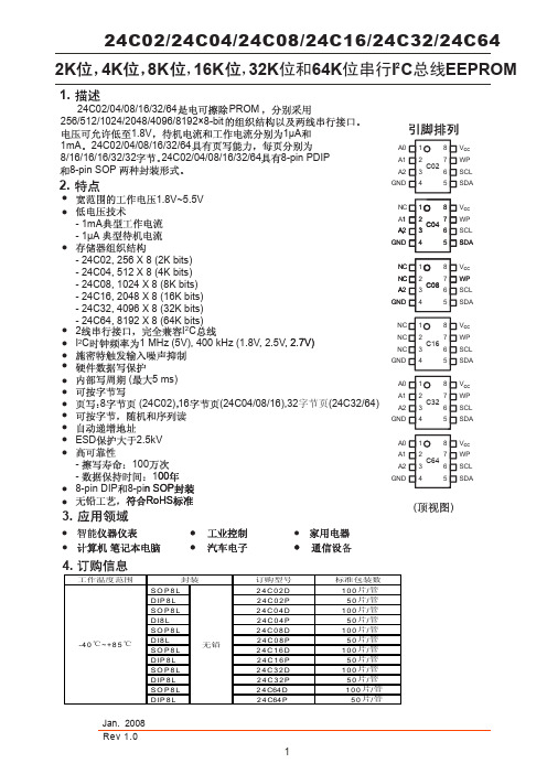
24C02/24C04/24C08/24C16/24C32/24C641.2.2K4K 8K ,16K ,32K 位和64K 位串行I C 总线EEPROM3.24C02/04/08/16/32/64PROM256/512/1024/2048/4096/8192×8-bit1.8V1μA1mA 24C02/04/08/16/32/648/16/16/16/32/3224C02/04/08/16/32/648-pin PDIP8-pin SOP ●●●●●●●●●●●●SD SCL WP V CC NC A SD A SCL WP V CC 12348765NC NC NC GND SD A SCL WP V CC 12348765 ()SD A SCL WP V CC 12348765A 0A 1A 2GND C02C1621.8V~5.5V- 1mA- 1μA- 24C02, 256 X 8 (2K bits)- 24C04, 512 X 8 (4K bits) - 24C08, 1024 X 8 (8K bits) - 24C16, 2048 X 8 (16K bits)- 24C32, 4096 X 8 (32K bits)- 24C64, 8192 X 8 (64K bits)2I CI C 1 MHz (5V), 400 kHz (1.8V, 2.5V, 2.7V) ( 5 ms)8 (24C02)16(24C04/08/16),32字节页(24C32/64)ESD 2.5kV - 100- 100 8-pin DIP 8-pin SOP RoHS ●●●●●●●22●S D A 123487651A 2GND NC NC C A 2GND C04C082.7V)00n SOP●●SD A SCL WP V CC 12348765A 0A 1A 2GND C32SD ASCL WP V CC 12348765A 0A 1A 2GNDC6424C02/24C04/24C08/24C16/24C32/24C645. Ḛ1 ḚV 6. 乱 ヺ ԡⳈ⌕կ⬉⬉ Ⳉ⌕䕧 ⬉ ⏽V CC Ⳉ⌕䕧 ⬉ V IN V OUT T STG -0.3 ~ V CC +0.3-0.3 ~ V CC +0.3-0.3 ~ +6.5°C -65 ~ +150V °C7. 㤤 ӊヺ ԡⳈ⌕կ⬉⬉ V CC ⏽T A+855.5 1.8-40(䍙 乱 㛑Ӯ 㟈 ӊ )V V ( 㤤 ӊϟ ⦄ 㛑)SDASCL WP V CCNC /NC /NC /A0NC /NC /A1/A1NC /A2/A2/A2C16/C08/C04/C02GNDSTART STOPLOGICSERIAL CONTROLLOGICDEVICE ADDRESS COMPARATORDATA WORD ADDRESS COUNTER LOADCOMPLOADINCY DECODER HIGH VOLTAGE PUMP/TIMING ENDATA RECOVERYEEPROMSERIAL MUXX D E C O D E RDOUT/ACKNOWLEDGEDINESD ⬉ (Ҏԧ )ESD ⬉ ( )V ESD2500200V V乱⬉ 䕧 ⬉ 乱 㛑Ӯ 㟈 ӊ DOUTmA 9. Ⳉ⌕⬉⇨⡍ヺ ԡ ⬉⌕կ⬉⬉⌕I CC V CC =5V⌟䆩 ӊ100kHz 3.0䕧 Ԣ⬉ ⬉μA 3.01.0-0.6V 0.4V IN = V CC GND 0.05( ӊ˖T A = 0°C ̚ +70°C, V CC = +1.8V ̚ +5.5V ˈ䰸䴲 ⊼䞞)䕧 Ԣ⬉ ⬉ μA V IL 0.4V CC0.20.4100kHz V V CC ×0.3I SB V IN = V CC GND V OUT = V CC GND μA 䕧 ⓣ⬉⌕䕧 ⓣ⬉⌕I LI I LO V IH 䕧 催⬉ ⬉ V CC +0.5V V V VV OL3V OL2V = 2.1 mA V 10. Ѹ⌕⬉⇨⡍ ( ӊ˖T A = 0°C ̚ +70°C, V = +1.8V +5.5V, C L = 100 pF ˈ䰸䴲 ⊼䞞)ヺ ԡ䩳催⬉䩳乥⥛, SCL ⌟䆩 ӊ400V CC =1.8V 1000ns 0.050.050.60.90.6 μskHz 1.20.5540V CC =5V 0.4t LOW μs ⍜䰸 䯈 䩳ϟ䰡⊓ 䕧 䯈䱨 䯈t I t AA50t HIGH䩳Ԣ⬉ μsV CC =1.8V V CC =5V V CC =1.8V V CC =5V V CC =1.8V V CC =5V V CC =1.8V V CC =5V8. 㛮⬉( ӊ˖T A = 25°C, f = 1.0 MHz, V CC = +1.8V)pFヺ ԡ䕧 /䕧 ⬉ (SDA)C I/O 䕧 ⬉ (A0, A1, A2, SCL)C IN68 pF⌟䆩 ӊV I/O = 0V V IN = 0V1.2 㒓䞞 䯈t BUF0.5μs V CC =1.8V V CC =5V䇏1.03.0 mA m 042.0C =5.0V, I OL = 3.0 mA CC ×0.7GNDOL1V CC =3.0V, I OL =2.1mA CC =1.8V, I OL = 0.15 mA =C CC = +1.8V ̚+5.5f SCL10. Ѹ⌕⬉⇨⡍ (㓁)䕧 Ϟ 䯈 䕧 䯈0ns500.650.25ns t WRns 100ns ℶ ӊ ゟ 䯈 䕧 䯈t R t DH t F 䕧 ゟ 䯈μs ms䕧 ϟ䰡 䯈t SU.STOV CC =1.8V V CC =5V V CC =1.8V V CC =5Vμs 300100300t HD.DAT t SU.DAT 2 㒓3SCLSDA_INSDA _OUTt F t LOWt SU .STAt HD.STAt AA t DHt BUFt SU.STOt Rt HD.DAT t SU.DAT t HIGH t LOW8th BIT SCLSDAACKSTOPCONDITIONSTART CONDITIONt WR (1)t HD.STAμs 䍋 ӊ 䯈䍋 ӊ ゟ 䯈t SU.STA V CC =1.8V V CC =5V V CC =1.8V V CC =5Vμs 0.60.250.60.25ヺ ԡ ⌟䆩 ӊ ⊼ 䯈W :5 ҢϔϾ ⱘ ℶ ӊ 㟇 䚼 㒧 ⱘ 䯈DŽn 08V μ3001AHIG11.3156247A0A1A2SDA SCL WP GND V CCA2A1A024C02/32/64A2A1A0824C02/32/6424C04A2A1424C04A024C08A2224C08A0A124C1616KA2A1A0/SDA V CC10kΩSCL8WP WPWPV CC12.13. 䆺㒚 䇈24CXX I C 㒓Ӵ䕧 䆂DŽI C ϔ⾡ ǃϸ㒓І㸠䗮䆃 ˈ І㸠 㒓SDA І㸠 䩳㒓SCL DŽϸḍ㒓䛑 乏䗮䖛ϔϾϞ ⬉䰏 ⬉⑤DŽ ⱘ 㒓䜡㕂 4 ⼎4 ϸ㒓 㒓䜡㕂㒓Ϟ 䗕 ⱘ ӊ㹿⿄ 䗕 ˈ ⱘ ӊ㹿⿄ DŽ Ѹ ⱘ ӊ㹿⿄Џ ӊˈ Џ ӊ ⱘ ӊ 㹿⿄Ң ӊDŽЏ ӊѻ⫳І㸠 䩳SCL ˈ㒓ⱘ䆓䯂⢊ ǃѻ⫳START STOP ӊDŽ24CXX I C 㒓ЁЎҢ ӊ DŽ㒓 Ѣぎ䯆⢊ ҹ Ӵ䕧DŽ↣ Ӵ䕧 ѢSTART ӊˈ㒧 ѢSTOP ӊˈѠ㗙П䯈ⱘ 㡖 ≵ 䰤 ⱘˈ⬅ 㒓ϞⱘЏ ӊ DŽ ҹ 㡖˄8ԡ˅Ў ԡӴ䕧ˈ9ԡ ⬅ ѻ⫳ ㄨDŽ䍋 ℶ ӊ䩳㒓䛑Ў催 ⿄ 㒓 ぎ䯆⢊ DŽ SCL Ў催⬉ SDA ⱘϟ䰡⊓˄催 Ԣ 䍋 ӊ˄START ˈㅔ ЎS ˅ˈSDA ⱘϞ ⊓˄Ԣ 催˅ ℶ ӊ˄STOP ˈㅔ ЎP ˅DŽ 㾕 5DŽ5 䍋 ӊ ℶ ӊⱘ НV CCҪ24Cxx MPU SDASCLR PR Pϸ㒓І㸠S Ў催ㅔ ЎⱘϞ ⊓˄Ԣ 㒓І㸠 㒓SS 䍋 ӊ222ԡӴ䕧↣Ͼ 䩳㛝 Ӵ䗕ϔԡ DŽSCL Ў催 SDA 乏 〇 ˈ Ўℸ SDA ⱘ 㹿䅸Ў DŽԡӴ䕧 㾕 6DŽ6 ԡӴ䕧ㄨ㒓Ϟⱘ ↣ ϔϾ 㡖 ѻ⫳ϔϾ ㄨˈЏ ӊ 乏ѻ⫳ϔϾ ⱘ乱 ⱘ 䩳㛝 ˈ㾕 7DŽ7 I C㒓ⱘ ㄨ ԢSDA 㒓㸼⼎ ㄨˈ ㄨ㛝 䯈 〇 ⱘԢ⬉ DŽ Џ ӊ ˈ 乏 Ӵ䕧㒧 ⱘ 㒭 䗕 ˈ ϔϾ 㡖П ⱘ ㄨ㛝 䯈ϡӮѻ⫳ ㄨ ˄ϡ ԢSDA ˅DŽ䖭⾡ ϟˈ 䗕 乏䞞 SDA 㒓Ў催ҹ Џ ӊѻ⫳ ℶ ӊDŽ䗕 䕧 ⱘ䕧 ⱘЏ ӊ ⱘ䍋 ӊ289䴲 ㄨㄨㄨ 䩳㛝㒓〇䆌SDASCL2ѻ⫳ϔϾ ㄨˈЏ ӊ 乏ѻ⫳ϔԢ㒓Ӵӊ ⱘSCL 䍋 ӊS1ӊ䍋 ӊՓ㛑㢃⠛䇏 ˈEEPROM 䛑㽕∖ 8ԡⱘ ӊ ˄㾕 8˅DŽӊ ⬅"1"ǃ"0" 㒘 ˈ 4ԡ Ё ⼎ˈ Ѣ І㸠EEPROM 䛑 ϔḋⱘ Ѣ24C02/32/64ˈ䱣 3ԡA2ǃA1 A0Ў ӊ ԡˈ 乏Ϣ⹀ӊ䕧 㛮 ϔ㟈DŽ Ѣ24C04ˈ䱣 2ԡA2 A1Ў ӊ ԡˈ 1ԡЎ义 ԡDŽA2 A1 乏Ϣ⹀ӊ䕧 㛮 ϔ㟈ˈ㗠A0 ぎ㛮DŽѢ24C08ˈ䱣 1ԡA2Ў ӊ ԡˈ 2ԡЎ义 ԡDŽA2 乏Ϣ⹀ӊ䕧 㛮 ϔ㟈ˈ㗠A1 A0 ぎ㛮DŽѢ24C16ˈ ӊ ԡˈ3ԡ䛑Ў义 ԡˈ㗠A2ǃA1 A0 ぎ㛮DŽ ӊ ⱘLSB Ў䇏/ 䗝 ԡˈ催Ў䇏 ˈԢЎ DŽ㢹↨䕗 ӊ ϔ㟈ˈEEPROM 䕧 ㄨ"0"DŽ ϡϔ㟈ˈ 䖨 ⢊ DŽ8 ӊ 1010A2A1A0R/W MSBLSB1010A2A1P0R/W1010A2P1P0R/W1010P2P1P0R/Wӊ EEPROM Ԣ 㗫 ⱘ⡍⚍ˈ ӊЎ˖˄1˅⬉⑤Ϟ⬉˗˄2˅ ℶ ӊ ӏԩ 䚼 DŽ24C0424C0824C16DŽ ԡ䆂Ёѻ⫳Ё ǃ ⬉ ㋏㒳 ԡ ˈI C 㒓 䗮䖛ҹϟℹ偸 ԡ˖ ˄1˅ѻ⫳9Ͼ 䩳 DŽ˄2˅ SCL Ў催 ˈSDA гЎ催DŽ ˄3˅ѻ⫳ϔϾ䍋 ӊDŽ21. 㡖㽕∖ ӊ ACK ㄨ ˈ 8ԡⱘ DŽ 䖭Ͼ EEPROM ㄨ"0"ˈ✊ ϔϾ8ԡ DŽ 8ԡ ˈEEPROM ㄨ"0"ˈ ⴔ 乏⬅Џ ӊ 䗕 ℶ ӊ 㒜ℶ DŽℸ EEPROM 䖯 䚼 t WR ˈ 䴲 Ёˈ ℸ 䯈 䕧 䛑 Ⳉ ˈEEPROM Ӯ ㄨ˄㾕 9˅DŽ9 㡖SDA 㒓䍋 ӊM S BL S B R /W A C K M S BL S B A C KA C Kӊℶ ӊDŽ24C02/32/6413.2.图10页写24C02器件按8字节/页执行页写,24C04/08/16器件按16字节/页执行页写,24C32/64器件按32字节/页执行页写。
- 1、下载文档前请自行甄别文档内容的完整性,平台不提供额外的编辑、内容补充、找答案等附加服务。
- 2、"仅部分预览"的文档,不可在线预览部分如存在完整性等问题,可反馈申请退款(可完整预览的文档不适用该条件!)。
- 3、如文档侵犯您的权益,请联系客服反馈,我们会尽快为您处理(人工客服工作时间:9:00-18:30)。
w 址输入脚 A0 A1 A2 可悬空或连接到 Vss 如果只有一个 24WC01 被总线寻址 这三个地址输入
脚 A0 A1 A2 必须连接到 Vss
当使用 24WC04 时最多可连接 4 个器件 该器件仅使用 A1 A2 地址管脚 A0 管脚未用 可以连
符号
参数
最小
典型
最大 单位
测试条件
ICC 电源电流
3
mA
FSCL=100KHz
ISB ILI ILO VIL VIH VOL1 VOL2
备用电流(Vcc=5.0V) 输入漏电流 输出漏电流 输入低电压 输入高电压 输出低电压 输出低电压
1 Vcc 0.7
0
A
10
A
10
A
Vcc 0.3 V
Vcc+0.5 V
s
tHD: DAT
数据输入保持时间
0
0
ns
tSUl: DAT
数据输入建立时间
50
50
ns
tR
SDA 及 SCL 上升时间
1
0.3
s
tF
SDA 及 SCL 下降时间
300
300
ns
tSU: STO
停止信号建立时间
4
0.6
s
tDH
数据输出保持时间
100
100
ns4Biblioteka 海纳电子资讯网: www.fpga-arm.com
上电时序
符号
参数
最大
单位
tPUR
上电到读操作
1
ms
tPUW
上电到写操作
1
ms
写周期限制
.
间
符号
参数
最小
典型
最大
单位
m tWR
写周期时间
10
ms
写周期时间是指从一个写时序的有效停止信号到内部编程/擦除周期结束的这一段时间 在写周期期
r 总线接口电路禁能 SDA 保持为高电平 器件不响应外部操作
功能描述
写保护
写保护操作特性可使用户避免由于不当操作而造成对存储区域内部数据的改写 当 WP 管脚接高时 整个寄存器区全部被保护起来而变为只可读取 CAT24WC01/02/04/08/16 可以接收从器件地址和字节地 址 但是装置在接收到第一个数据字节后不发送应答信号从而避免寄存器区域被编程改写
.
图 6 字节写时序
m
r
a
-
a 页写
用页写 CAT24WC01 可一次写入 8 个字节数据 CAT24WC02/04/08/16 可以一次写入 16 个字节的
g 数据 页写操作的启动和字节写一样 不同在于传送了一字节数据后并不产生停止信号 主器件被允许
发送 P CAT24WC01 P=7 CAT24WC02/04/08/16 P=15 个额外的字节 每发送一个字节数据后
128/256/512/1024/2048 个 8 位字节 CATALYST 公司的先进 CMOS 技术实质上减少了器件的功耗
f CAT24WC01 有一个 8 字节页写缓冲器 CAT24WC02/04/08/16 有一个 16 字节页写缓冲器
I2C 总线接口进行操作 有一个专门的写保护功能
该器件通过
CAT24WC01/02/04/08/16 再根据读写控制位 R/W 的状态进行读或写操作
应答信号
I2C 总线数据传送时 每成功地传送一个字节数据后 接收器都必须产生一个应答信号 应答的器 件在第 9 个时钟周期时将 SDA 线拉低 表示其已收到一个 8 位数据
.
m CAT24WC01/02/04/08/16 在接收到起始信号和从器件地址之后响应一个应答信号 如果器件已选择
收 的模式 通过器件地址输入端 A0 A1 和 A2 可以实现将最多 8 个 24WC01 和 24WC02 器件 4 个
g 242C04 器件,2 个 24WC08 器件和 1 个 24WC16 器件连接到总线上
管脚描述
SCL 串行时钟
p
f CAT24WC01/02/04/08/16 串行时钟输入管脚用于产生器件所有数据发送或接收的时钟 这是一个输
0.4
V
0.5
V
VIN=0 ~Vcc VIN=0 ~Vcc VOUT=0 ~Vcc
m.
r IOL=3 mA a IOL=1.5 mA
分布电容
TA=25 , f =1.0MHz, Vcc =5V
符号
测试项
CI/O
I/O 电容 SDA 脚
CIN
输出电容 A0 A1 A2 SCL WP
-
最大
a 8 g 6
当使用 24WC16 时最多只可连接 1 个器件 所有地址管脚 A0 A1 A2 都未用 管脚可以连接到
Vss 或悬空
WP 写保护
如果 WP 管脚连接到 Vcc 所有的内容都被写保护 只能读 当 WP 管脚连接到 Vss 或悬空 允许
器件进行正常的读/写操作
I2C 总线协议
I2C 总线协议定义如下
5
w 各管脚承受电压 -2.0 Vcc+2.0V
Vcc 管脚承受电压 -2.0 +7.0V
封装功率损耗 Ta=25
1.0W
焊接温度(10 秒) 300
输出短路电流 100mA
可靠性参数
符号
参数
NEND TDR VZAP ILTH
耐久性 数据保存时间 ESD 上拉电流
最小 1,000,000
100 2000 100
应答信号后 主器件发送 CAT24WC01/02/04/08/16 的字节地址 主器件在收到从器件的另一个应答信号
后 再发送数据到被寻址的存储单元 CAT24WC01/02/04/08/16 再次应答 并在主器件产生停止信号后 开始内部数据的擦写 在内部擦写过程中 CAT24WC01/02/04/08/16 不再应答主器件的任何请求
a
- CAT24WC01/02/04/08/16 支持 I2C 总线数据传送协议 I2C 总线协议规定 任何将数据传送到总线的
器件作为发送器 任何从总线接收数据的器件为接收器 数据传送是由产生串行时钟和所有起始停止信
a 号的主器件控制的 主器件和从器件都可以作为发送器或接收器 但由主器件控制传送数据 发送或接
a
图 4 应答时序
-
a
g
p
f
图 5 从器件地址位
w.
w
w
1. A0 A1 和 A2 对应器件的管脚 1 2 和 3 2. a8 a9 和 a10 对应存储阵列地址字地址
7
海纳电子资讯网: www.fpga-arm.com
写操作
字节写
在字节写模式下 主器件发送起始命令和从器件地址信息 R/W 位置零 给从器件 在从器件产生
入管脚
. SDA 串行数据/地址
CAT24WC01/02/04/08/16 双向串行数据/地址管脚用于器件所有数据的发送或接收 SDA 是一个开漏
w 输出管脚 可与其它开漏输出或集电极开路输出进行线或 wire-OR A0 A1 A2 器件地址输入端
w 这些输入脚用于多个器件级联时设置器件地址 当这些脚悬空时默认值为 0 24WC01 除外
a
-
a
g
p
f
.
w
w
w
1
海纳电子资讯网: www.fpga-arm.com
CAT24WC01/02/04/08/16 1K/2K/4K/8K/16K 位串行 E2PROM
特性
.
与 400KHz I2C 总线兼容 1.8 到 6.0 伏工作电压范围
m
低功耗 CMOS 技术 写保护功能 当 WP 为高电平时进入写保护状态
6
海纳电子资讯网: www.fpga-arm.com
1 个 CAT24WC16 可单独被系统寻址 从器件 8 位地址的最低位 作为读写控制位 1 表示对从器件
进行读操作 0 表示对从器件进行写操作 在主器件发送起始信号和从器件地址字节后
CAT24WC01/02/04/08/16 监视总线并当其地址与发送的从地址相符时响应一个应答信号 通过 SDA 线
r
页写缓冲器 自定时擦写周期
a
1,000,000 编程/擦除周期 可保存数据 100 年
-
8 脚 DIP SOIC 或 TSSOP 封装 温度范围 商业级 工业级和汽车级
a
概述
g
p CAT24WC01/02/04/08/16 是 一 个 1K/2K/4K/8K/16K 位 串 行 CMOS E2PROM 内 部 含 有
100
400
KHz
200
200
ns
tAA tBUF
w SCL 变低至 SDA 数据输出及应答信号
新的发送开始前总线空闲时间
4.7
3.5
1.2
1
s s
tHD: STA
起始信号保持时间
4
0.6
s
tLOW
时钟低电平周期
4.7
1.2
s
tHIGH
时钟高电平周期
4
0.6
s
tSU: STA
起始信号建立时间
4.7
0.6
管脚配置
.
w
w
管脚描述
管脚名称
w功能
A0 A1 A2
器件地址选择
SDA
串行数据/地址
SCL
串行时钟
WP
写保护
Vcc