英飞凌模块的并联使用
英飞凌IGBT模块安装说明应用笔记

若需获得关于技术、交付条款和价格的更多信息,敬请联系距离您最近的英飞凌办事处()
警告
由于技术要求,组件可能包含有害物质。若需了解相关物质的类型,请联系距离您最近的英飞凌办事处。如果 可以合理地预计英飞凌的某个组件可能会导致生命支持设备或系统失效,或者影响该等设备或系统的安全性或 有效性,那么在将该等组件用于生命支持设备或系统之前,必须获得英飞凌的明确书面同意。生命支持设备或 系统意指用于植入人体内部,或者支持和/或维持、维系和/或保护人类生命的设备或系统。如果这些设备或系 统失效,可以合理地假设其用户或其他人的健康将受到威胁。 AN 2006-05 修订记录:2011 年 1 月 31 日 V2.0 先前版本:2006 年 7 月 1 日 V1.0 在上一版本的基础上作出的主要更改:一般修订;采用 PressFIT 技术安装 PCB 电路板:第二章第 5-11 页 全部:第二次发布 作者:Martin Knecht(IFAG IMM INP MP)
1.2 静电敏感元件的处理
IGBT 模块是静电敏感元件。静电放电(ESD)可能导致这些模块被过早损坏甚至毁坏。 为了防止静电放电造成元件毁坏或过早损坏,所交付的元件均采用了适当的静电防护封装,符合公认的 ESD 法规要求。 要拆卸静电防护装置,处理未受保护的模块,必须在符合 ESD 法规要求的工作场所中执行。如需了解 更多信息,请参考诸如 IEC 61340-5-1 和 ANSI/ESD S2020 等 ESD 安装准则。
图 2: EconoDUAL™ 3 模块上的 PCB 电路板安装支脚(红圈)
-5-
N 2010-03 2009
应用笔记 AN 2006-05 V2.0,2011年1月
取决于所安装的具体 PCB 电路板的厚度和重量,拧入 PCB 电路板安装支脚内的有效螺纹长度应当至少 为 lmin 4 毫米,且最长不超过 lmax 10 毫米。
手把手教你学会模块电源并联均流主从设置法

手把手教你学会模块电源并联均流主从设置法在昨天的技术文章介绍中,我们详细的分析了如何利用输出阻抗法实现模块电源并联均流。
然而,这种方法在实际工作中存在很多缺陷,这就需要工程师合理进行选择。
今天要为大家介绍的是利用主从设置法完成电源模块并联并实现均流的方式,希望能够通过本文的介绍,帮助工程师更好的完成多电源模块并联工作。
所谓的主从设置法,指的是在并联的n个变换器模块中,通过人为的程序制定,将这些电源其中的一个指定为主模块,而其余各模块跟从主模块分配电流,称为从模块。
该方法适用于有电流型控制的并联开关电源系统中,电流型控制是指开关电源模块中有电压控制和电流控制,电流环为内环,电压环为外环。
下图为n个变换器模块并联的主从控制原理图。
图为主从模块设置法均流控制原理图 从上图中我们可以很清楚的看到,图中每个电源模块珺为双环控制系统,在这种控制系统中,工程师将模块l设定为主模块并使其按电压控制规律工作,其余的n一1个模块按电流型控制方式工作。
vr为主模块的基准电压,Vf为输出电压反馈信号。
经过电压误差放大器,得到误差电压Ve,它是主模块的电流基准,与Vll(该参数反映主模块电流Il大小)比较后,产生控制电压Vc,控制调制器和驱动器工作。
主模块电流将按电流基准vc调制,即模块电流近似与ve成正比。
在完成并联设置后,各个从模块的电压误差放大器接成跟随器的形式,主模块的电压误差ve输入各跟随器,跟随器输出均为Ve,为从模块的电流基准,因此各个从模块的电流均按同一Vc值调制,与主模块电流基本一致,从而实现模块间的均流。
总结 在模块电源的并联均流设计中,采用主从模块设置法能够较好的保障机体实现稳定高效工作,且不会出现电流分配特性差等问题。
但是它也有一些缺点,那就是该均流法要求主从模块间必须有通讯联系,所以整个系统比较复杂。
且如果主模块失效,则整个电源系统不能工作,因此可靠性取决于主模块,只能均流,不适用于构成冗余并联系统。
IGBT模块的并联使用技术指南

Paralleling of modules or paralleling of inverters becomes necessary, if a desired inverter rating or output current can not be achieved with a single IGBT module as switch.From an economic point of view paral-leling of modules is in many cases the solution of choice. On the other hand it is a technical challenging task to ensure proper current sharing between the parallel connected modules.This application note shades light on the technical measures which help to ensure a homogenous current sharing within the parallel connected power modules. Homogenous current sharing is also the key to maintain high ruggedness of the whole converter and it allows an optimal utilisation of the power modules with minimal de-rating.Paralleling of IGBT modules IGBT模块的并联应用ContentsPage1 Introduction 32 Static current sharing 32.1 Influence of the module parameter spread 32.2 External influence on current sharing 43 Dynamic current sharing 43.1 Common Gate-Driver 43.2 Common Gate-Driver with common mode chokes 53.3 Individual Gate-Driver 63.4 Stray Inductance and Clamping 73.5 Phase connection 8 3.6 Influence of the junction Temperature 83.7 Influence of the device parameters 94 General recommendations / Summary 94.1 De-rating 95 References 91 IntroductionIn an ideal case the current capability of IGBT modules scales with the number of modules connected in parallel. Due to a never completely matched impedance of each module connection and due to parameter variations between the different modules a per-fect current sharing is not realistic. In addition unequal cooling of the semiconductor devices can lead to further current imbalance in and between the modules since the semi-conductor on-state and switching characteristics are temperature dependent. This application note deals with the influence parameters for static and dynamic current sharing and shows the impact on current imbalance between the parallel connected modules and con-sequential influence on the junction temperature.2 Static current sharingThe static current sharing is influenced mainly by the difference of the connection resistance and the on-state characteristics of the parallel connected modules.Figure 1 shows the simplified electrical circuit for two parallel connected modules assuming a linear approximation of the on-state characteristics of the modules. The connection resistance for each module is lumped in a simple resistor. The value of this resistor is strongly customer application specific.2.1 Influence of the module parameter spreadFigure 2 shows the IGBT -on state voltage distribution of a produc-tion time of roughly one year for one product. The median V CEsat of the population is at 5.4 V and the standard deviation is 0.065 V .In order to statistically evaluate the current sharing of two parallel connected modules the V CEsat of roughly 4000 measured modules was randomly grouped into a total of 200 pairs.Figure 3 shows the probability plot of the V CEsat difference of the paralleled IGBT modules. The random grouping of the modules out of the population shown in Figure 2, yields in a median V CEsat difference of 65 mV and a maximum difference of 265 mV .More important than the voltage difference, is the resulting current imbalance between the paralleled modules.In order to calculate the current in the modules a linear approxi-mation of V CEsat versus I C was assumed between nominal current (600 A) and 1/3 of the nominal current (see also Figure 1).Eqn. 1As a simplification the threshold on-state voltage (V TO ) at zero amps was set to 2.5 V . This is quite close to the reality since most of the process variations influence more the resistive part of the characteristics and only minor the V TO . Evaluating only the current imbalance due to the module variation, (assuming the worst case of zero connection resistance) both paralleled modules must see the same voltage drop. Running two paralleled modules at twice the nominal rating of a single module will cause a common voltage drop of the average V CEsat of the two modules at its nominal current (in the example 600 A per module). Thus the resulting module current in each module can be calculatedFigure 1: On-state modelFigure 2: Statistics of the IGBT on-state (6500 V / 600 A module)Figure 3: Statistics of VCEsat difference between paralleled modules (6500 V / 600 A module)delta_VCEsatP r o b a b i l i t yVCEsat @ 600A, 125 °CP r o b a b i l i t y+1s-1s +2s-2s +3s-3s m e d i a nEqn. 2Figure 4: Current imbalance (6500 V / 600 A module)based on its on-resistance (r CE ):The current imbalance between the paired modules from Figure 3 is expressed as the maximum collector current minus theaverage current, divided by the average current (in this example 600 A). The probability plot of the current imbalance of two paralleled modules is shown in Figure 4. The median current imbalance is 1.1 % and the maximum observed current imbalance was 4.5 %.The current sharing shown in Figure 4 is what can be expected if modules from a large production period (one year) are randomly grouped in to pairs, excluding the influence of possibleinhomogenous cooling and connection resistance. A furtherimprovement in static current sharing can be achieved if the mod-ules for parallel connection are specifically selected based on its on-state voltage (V CEsat / V F ) or if modules from the same produc-tion lot (narrower parameter spread) are used. Figure 5 shows the current imbalance as a function of the on-state voltage difference.2.2 External influence on current sharingThe influence of the connection resistance can be calculated straight forward based on the model shown in Figure 1.Especially for semiconductors with low on-state voltage and thusFigure 5: Current imbalance vs. VCEsat (6500 V / 600 A module)(Ic,max-Ic,av)/Ic,avP r o b a b i l i ty0.050.10.150.20.250.3delta_VCEsat(I c ,m a x -I c ,a v )/I c ,a vlow on-resistance the connection resistance can have a signifi -cant influence on current sharing which is at least in the same range as the module characteristic influence.Beside the connection resistance also the cooling has aninfluence on current sharing. Since the semiconductor on-state characteristics are more or less temperature dependent.Figure 6 shows the on-state characteristics for 25 and 125 °C of a 6500 V 600 A IGBT. Obviously if one module would be oper-ated at 25 °C and the other module at 125 °C, the cooler module would take a much larger share of the total current. Though thanks to the positive temperature coefficient the currentsharing in reality would improve since the higher current in the cold module would cause a higher temperature and vice versa for the hotter module. So in short time the current sharing would stabilise. Nevertheless homogenous cooling with the same in-let temperature of the cooling medium for both module heat-sinks is crucial. Especially for the diode operation mode, since the diode on-state characteristic does not offer necessarily a positive tem-perature coefficient over the full current and temperature st but not least also the gate voltage supplied by the gate-unit has an influence on the on-state char-acteristics of the IGBT. It is thus important that the gate-voltages are narrowly matched for all parallel connected IGBTs or that the same gate-voltage supply is used.3 Dynamic current sharingDynamic current sharing depends largely on the external power circuit design. Especially during the turn-on process different emitter impedance values to the common point of the commuta-tion loop have a strong influence since the gate-voltages of the paralleled IGBTs are directly affected if a common gate-driver for all modules is used. If individual gate drivers are used, proper matching and narrow parameter spread between the drivers is crucial.3.1 Common Gate-DriverFigure 7 shows a simplified schematic of a parallel connection of two IGBT modules with a common Gate-Unit and with slightly different connection inductance values which resemble a not ideal but realistic difference to the virtual common connection point for this consideration. Through this configuration a loop between theFigure 6: IGBT on-state characteristics (6500 V / 600 A module)Figure 7: Simplified schematic of a parallel connectionunavoidable.Especially during turn-on this has a significant influence on the dynamic current sharing. Assuming an identical initial turn-on di C/ dt we get a proportional voltage drop across the stray inductance between the auxiliary emitter potential and the common point (marked as earth symbol in Figure 7):Eqn. 3 This unequal potential of the two auxiliary emitters forces a current through the auxiliary emitter connection to the gate-unit. Consequently we get a voltage drop across the impedance of this connection (Z E) which changes the effective gate voltage as shown in Figure 7. In the example the gate voltage for the left IGBT with lower emitter inductance will be lifted and the gate voltages for the right IGBT will be damped. Thus the left IGBT takes most of the initial current and thus also produces signifi-cantly higher turn-on losses. Figure 8 shows a simulated turn-on behaviour with two 3300 V / 1200 A IGBTs and unequal connec-tion as shown in Figure 7. Obviously the current mismatch is quite significant which causes roughly 20 .. 25 % higher turn-on losses for the left switch compared to the expected losses with ideal current sharing.Needless to say that this severe current mismatch is far from being ideal, thus the current and losses mis-match needs to be translated into a proper de-rating if the design of the power circuit can not be improved.Interestingly the effect on turn-off is nearly invisible since the gate-voltage has practically no influence on the turn-off current characteristics and the theoretical influence on the collector voltage is irrelevant since the voltages are forced to be identical by definition. Figure 9 shows a turn-off event. The influence of the unequal L sE on V GE is clearly visible, but it has negligible influence on the collector current and thus the overall characteristics.3.2 Common Gate-Driver with common mode chokesA patented method from ABB to rectify unequal connection impedance values is the use of so called common mode chokes. The common mode chokes nearly don’t influence the gate-emit-Figure 8: IGBT turn-on with unequal emitter inductanceFigure 9: IGBT turn-off with unequal emitter inductanceFigure 10: Parallel connection with common mode chokesFigure 11a: Turn-on with common mode chokesIn Figure 10 a simplified schematics of a parallel connection with common mode chokes in the gate is shown. Since the common mode chokes decouple the gate-unit from the IGBT emitter it is important to tap one emitter with a resistance (RE ~ 100 m ) to the gate-unit in order to facilitate a proper V CEsat measurement for the desaturation detection.ns delay between the gates from IGBT1 to IGBT2. As a result we get a significant dynamic current mismatch in terms of amplitude and delay. Thus the turn-on and the turn-off losses deviate up to 15 .. 20 % from the expected switching losses with ideal current sharing. In addition the turn-off current is 40 % above the average turn-off current. It is a must to consider this in the SOA derating of the paralleled IGBT modules.Figure 13: Turn-off with 100 ns timing mismatchFigure 14: Turn-on with 0.5 V VGE mismatchIn Figure 14 and Figure 15 the turn-on respective the turn-off switching with 0.5 V difference in V GE are shown. Even if V GE seems to have less influence in dynamic current sharing it needs to be considered, especially for the turn-on losses (E on ), where the mis-match of this example is still 5 .. 10 %.3.4 Stray Inductance and ClampingFor reliable device operation it is crucial, that the peak voltage even during switching always stays below the maximum rated device voltage. Especially if high current modules are parallel con-nected, this can become a challenge for the power electronics age and the switching speed (di/dt) and the stray inductane (L ):Eqn. 5Eqn. 6of the paralleled modules at a similar -. Especially for high-current modules sor diodes between gate- and emitter and as well as a Schottky diode to the +15 V supply) and gate-resistor. Advanced active clamping with feedback to the final amplifier stage of the gate-unit (indicated with dashed lines) is strongly recommended in order to avoid overload to the suppressor diodes.Figure 16: Active ClampFigure 17: De-coupling with phase inductorsFigure 18: Phase current harmonising with chokesFigure 19: SOA turn-off IGBT1 @ 105 °C / IGBT2 @ 125 °C3.5 Phase connectionAdditional current balancing between paralleled modules can be achieved with the introduction of additional impedance in the phase connection, which decouples the single modules (Figure 17).This solution though has the disadvantage that the converter needs to supply the additional reactive power consumed by the inductors.An even better alternative to the single phase inductors is tomagnetic couple the phase currents with chokes that can be built with ferrite cores (Figure 18). In this case the inductance has only an effect on the current difference between the paralleled phase-legs.3.6 Influence of the junction TemperatureThe junction temperature has a significant influence on theswitching characteristics and thus the dynamic current sharing. Especially during turn-off it is crucial to ensure, that all modules are operated within its safe operating area. In order to investigate the dynamic current sharing, special measurements carried out on 3300 V / 1200 A SPT modules with by purpose varied junction temperatures have been carried out [2]. The test was done with a total stray inductance of 100 nH (200 nH/module) and with the use of common mode chokes (Figure 10) in order to minimize the influence of the power circuit:Ic1Ic2IctotVc VGEEoff2Eoff1123456kA0.51.01.52.02.53.03.5kV -15-10-5051015V123456789J 3456789µsFigure 20: SOA turn-off IGBT1 @ 25 °C / IGBT2 @ 125 °CFigure 19 and Figure 20 show the current sharing during turn-offat extreme switching conditions. As expected the cold module carries more current before the turn-off event is initiated (static current sharing). Though the hot module dissipates more turn-off energy since the current during turn-off commutates to the hot module (more charge). As a matter of fact the hot module will be heated even more so from the turn-off point of view no stabilisation effect is to be expected.Thus it is crucial to design homogenous heatsinks that cool both modules identical, even if this test demonstrates the excellent robustness of the SPT technology.3.7 Influence of the device parametersIn principle the main influence parameters that cause currentimbalance between parallel connected modules are the switching times, respective the IGBT turn-on and turn-off delay times and the transfer characteristics (pinch-off voltage). In practice the dis-tribution of the switching delay times are narrow and in the range of the measurement accuracy of production test equipment. The main contribution for current imbalance can be attributed to the difference in pinch-off voltage (V p ) between the paralleled IGBTs. Different pinch-off voltages on the other hand are also the main contributor to the delay time variations between different IGBTs. Since the pinch-off voltage is a static parameter that can be measured accurate it is usually the parameter which is used if a selection of modules for paralleling is desired. The impact of different pinch-off voltages of paralleled devices can be simulated by varying the gate-voltage (V GEon ) of the gate-unit since this has practically the same effect as different V p . Figure 14 and Figure 15 in the chapter 3.3 thus show expected effect of a 0.5 V mismatch in V p (a 0.5 V higher V GE is similar than a 0.5 V lower V p ). Again the effect on turn-on is much more pronounced than in case of turn-off.At last of course the turn-off respectively diode recovery losses of the individual switches still follow the classic technology curve (E off vs. V CEsat – E rec vs . V F ). As E off and E rec are indirect proportional to the conduction losses, the switching losses mismatch is compen-sating the static losses mismatch to some extend. Still a narrow parameter spread in V CEsat and V F helps to improve both, static and dynamic current sharing.Ic1Ic2Ictot Vc VGEEoff2Eoff1123456kA0.51.01.52.02.53.03.5kV -15-10-5051015V2468101214J3456789µs4 General recommendations / SummaryIn order to achieve an equal current sharing between paralleled modules homogenous cooling is crucial in order to maintain a close matching of the junction temperatures of the individual modules and to avoid possible thermal runaway. Additionally a very symmetric construction of the power circuit with identical connection impedance values for each module is an absolute must.In Table 1 typical losses and current mismatches are shown for a parallel connection of two IGBT modules. Obviously the module parameter spread has much less impact than the influence of asymmetrical connection impedance or gate-driver variations.In addition the module parameter spread can be reduced by asuitable device selection with the parameters V CEsat /V F and V p . It though makes sense to verify if the selection of modules for parallel connection makes sense from an economic point of view. The benefit of less de-rating due to device selection should be compared to the costs involved for the logistics of the device selection and possible write-offs for unmatchable components.4.1 De-ratingThe de-rating of modules in parallel connection should be done based on two kinds of considerations:Safe-Operating-AreaThe modules must always be operated within the safe operating area (SOA). The main topic to look at, are the switching currents. Table 1 for instance shows a current imbalance of up to 50 % in the turn-off current in case of switching delays caused by the gate-unit. In such a case the maximum turn-off current must be reduced by 50 % in order to stay inside the SOA.Thermal de-ratingNot homogenous current sharing causes higher losses in the module that takes more current. Consequently this needs to be considered in case of parallel operation. For the on-state losses the current mismatch can be expressed by multiplying the on-state losses with the factor for the current imbalance (e.g. D = 1.05 for 5 % current mismatch).Eqn. 7The same is true for the switching losses. If the losses mismatch is known it has to be considered for the total switching lossesA p p l i c a t i o n n o t e 5S Y A 2098-00 25.08.2013NoteWe reserve the right to make technical changes or to modify the contents of this document without prior notice.We reserve all rights in this document and the information contained therein. Any reproduction or utilisation of this document or parts thereof for commercial purposes without our prior written consent is forbidden.Any liability for use of our products contrary to the instructions in this document is excluded.Eqn. 8Figure 21 shows the output current of two paralleled and fully utilised 6500 V 600 A modules operated at its maximum junc-tion temperatures. The solid line represents the achievable output current without any de-rating in inverter operation. The dashed lines show the reduced output current due to de-rating caused by module parameter variations. No de-rating due to the circuit parameters is considered, thus a perfect symmetrical power circuit is assumed. For the selected modules a delta V CEsat /V F of 100 mV (corresponding to 2 % current static current imbalance) and dynamic switching loss mismatch of 2.5 % (E off + E on ) are as-sumed. For the randomly picked unselected modules a static current imbalance of 5 % and a dynamic losses mismatch of5 % are assumed. This yields in a switching frequency dependent output current de-rating of 1.5 .. 2.5 % for the selected module and 3.5 .. 5 % for the unselected module. The switchingfrequency dependency comes from the fact that the dynamic losses mismatch gets dominant at higher switching frequencies. This has to be especially considered for dynamic current mis-match due to unsymmetrical power circuit connection or timingvariations of the gate-drivers, which is not included in Figure 21.Figure 21: Output current de-ratingVersion ChangeAuthors00 Initial release Raffael Schnell5 References[1] R. Schnell, U. Schlapbach, K. Haas, G. Debled,«Parallel Operation of LoPak Modules», Proc. PCIM’03, Nuremberg[2] U. Schlapbach, M. Rahimo, A. Baschnagel, A. Kop-ta, E. Carroll, «Switching-Self-Clamping-Mode «SSCM» for Over-voltage Protection in High Voltage IGBT Applica-tions»,Proc. PCIM’05, Nuremberg6 Revision history。
英飞凌igbt模块安装应用笔记

英飞凌igbt模块安装应用笔记英飞凌igbt模块安装应用笔记作者:微叶科技时间:2015-12-01 15:581 英飞凌igbt模块安装应用概述1.1 一般应用信息通过在生产过程中执行适当的可靠性测试和100%最终测试,确保符合英飞凌IGBT模块要求。
IGBT模块产品数据表和应用笔记中给出的最大值,均为不得超出的规定限值,哪怕只是短时超限也不允许,因为这会导致元件损坏。
本应用笔记未能涵盖所有不同应用和应用条件。
因此,应用笔记不能替代用户执行的细致深入的技术评估和检查。
因此,不论在任何情况下,应用笔记均不应构成任何供应商同意的保证的一部分,除非供应协议以书面方式另行规定。
1.2 静电敏感元件的处理IGBT模块是静电敏感元件。
静电放电(ESD)可能导致这些模块被过早损坏甚至毁坏。
为了防止静电放电造成元件毁坏或过早损坏,所交付的元件均采用了适当的静电防护封装,符合公认的ESD法规要求。
要拆卸静电防护装置,处理未受保护的模块,必须在符合ESD法规要求的工作场所中执行。
如需了解更多信息,请参考诸如IEC61340-5-1和ANSI/ESDS2020等ESD安装准则。
图1:静电放电标志2 将PCB电路板安装到模块上的说明2.1将PCB电路板安装到可焊模块上的说明2.1.1额外加固印刷电路板利用外接驱动板,可实现尽可能短的栅极-集电极连接,以防止磁耦合,并最大限度地降低栅电路的寄生电感。
完成焊接之后,建议采用机械方法,消除模块与印刷电路板之间的应力。
可以利用自攻螺丝或类似的紧固方法,通过模块上的4个PCB电路板安装支脚(请参见图2),将PCB电路板安装到模块上,以消除应力。
如需进一步的技术支持,可应要求提供评估驱动板和评估模块适配器板(模块适配器用于连接栅极电阻和箝位二极管)。
关于EconoDUAL?评估驱动板的更多信息,请参考应用笔记AN2006-04《面向EconoDUAL?IGBT模块的评估驱动板》。
正确理解IGBT模块规格书参数
正确理解IGBT模块规格书参数本文将阐述IGBT模块手册所规定的主要技术指标,包括电流参数、电压参数、开关参数、二极管参数及热学参数,使大家正确的理解IGBT模块规格书,为器件选型提供依据。
本文所用参数数据以英飞凌IGBT模块FF450R17ME3 为例。
一、电流参数1. 额定电流(IC nom)大功率IGBT模块一般是由内部并联若干IGBT芯片构成,FF450R17ME3内部是3个150A 芯片并联,所以标称值为450A额定电流可以用以下公式估算:Tjmax–TC= VCEsat·IC nom·RthJCVCEsat 是IC nom的函数,见规格书后图1,采用线性近似VCEsat=(IC nom+287)/310 Tjmax=150℃,TC=80℃,RthJC =0.055K/W计算得:IC nom=500A2. 脉冲电流(Icrm 和Irbsoa)Icrm是可重复的开通脉冲电流(1ms仅是测试条件,实际值取决于散热情况)Irbsoa 是IGBT可以关断的最大电流所有模块的的Icrm和Irbsoa都是2倍额定电流值3. 短路电流ISC短路条件:t<10μs,Vge<15V,Rg>Rgnom(规格书中的值),Tj<125℃短路坚固性ØIGBT2为平面栅IGBT:5-8倍ICØIGBT3/IGBT4为沟槽栅IGBT:4倍IC二、电压参数1. 集电极-发射极阻断电压Vces测量Vces时,G/E两极必须短路Vces为IGBT模块所能承受的最大电压,在任何时候CE间电压都不能超过这一数值,否则将造成去器件击穿损坏Vces和短路电流ISC一起构成了IGBT模块的安全工作区:RBSOA图由于模块内部寄生电感△V=di/dt*Lin 在动态情况下,模块耐压和芯片耐压有所区别2. 饱和压降VCEsatIFX IGBT的VCEsat随温度的升高而增大,称为VCEsat具有正温度系数,利于芯片之间实现均流VCEsat 是IC的正向函数,随增大而增大ICVCEsat的变化VCEsat随IC的增大而增大VCEsat随VG的减小而增大VCEsat 值可用来计算导通损耗对于SPWM 控制, 导通损耗是:三、开关参数1. 内部门极电阻RGint为了实现模块内部芯片的均流,模块内部集成了内部门极电阻。
英飞凌 FP50R12N2T7P EconoPIM 2 模块 数据表
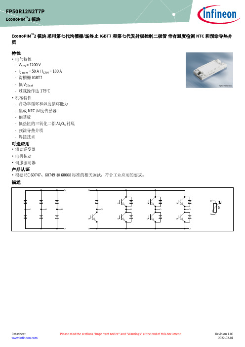
EconoPIM ™2 模块 采用第七代沟槽栅/场终止IGBT7和第七代发射极控制二极管 带有温度检测NTC 和预涂导热介质特性•电气特性-V CES = 1200 V-I C nom = 50 A / I CRM = 100 A -沟槽栅IGBT7-低 V CEsat-过载操作达175°C•机械特性-高功率循环和温度循环能力-集成NTC 温度传感器-铜基板-低热阻的三氧化二铝 Al 2O 3 衬底-预涂导热介质-焊接技术可选应用•辅助逆变器•电机传动•伺服驱动器产品认证•根据 IEC 60747、60749 和 60068标准的相关测试,符合工业应用的要求。
描述FP50R12N2T7PEconoPIM ™2 模块内容描述 . . . . . . . . . . . . . . . . . . . . . . . . . . . . . . . . . . . . . . . . . . . . . . . . . . . . . . . . . . . . . . . . . . . . . . . . . . . . . . . . . . . . . . . . .1特性 . . . . . . . . . . . . . . . . . . . . . . . . . . . . . . . . . . . . . . . . . . . . . . . . . . . . . . . . . . . . . . . . . . . . . . . . . . . . . . . . . . . . . . . . .1可选应用 . . . . . . . . . . . . . . . . . . . . . . . . . . . . . . . . . . . . . . . . . . . . . . . . . . . . . . . . . . . . . . . . . . . . . . . . . . . . . . . . . . . .1产品认证 . . . . . . . . . . . . . . . . . . . . . . . . . . . . . . . . . . . . . . . . . . . . . . . . . . . . . . . . . . . . . . . . . . . . . . . . . . . . . . . . . . . .1内容 . . . . . . . . . . . . . . . . . . . . . . . . . . . . . . . . . . . . . . . . . . . . . . . . . . . . . . . . . . . . . . . . . . . . . . . . . . . . . . . . . . . . . . . . .2 1封装 . . . . . . . . . . . . . . . . . . . . . . . . . . . . . . . . . . . . . . . . . . . . . . . . . . . . . . . . . . . . . . . . . . . . . . . . . . . . . . . . . . . . . . . . .3 2IGBT, 逆变器 . . . . . . . . . . . . . . . . . . . . . . . . . . . . . . . . . . . . . . . . . . . . . . . . . . . . . . . . . . . . . . . . . . . . . . . . . . . . . . . . .3 3二极管,逆变器 . . . . . . . . . . . . . . . . . . . . . . . . . . . . . . . . . . . . . . . . . . . . . . . . . . . . . . . . . . . . . . . . . . . . . . . . . . . . . . .5 4二极管,整流器 . . . . . . . . . . . . . . . . . . . . . . . . . . . . . . . . . . . . . . . . . . . . . . . . . . . . . . . . . . . . . . . . . . . . . . . . . . . . . . .6 5IGBT, 斩波器 . . . . . . . . . . . . . . . . . . . . . . . . . . . . . . . . . . . . . . . . . . . . . . . . . . . . . . . . . . . . . . . . . . . . . . . . . . . . . . . . .7 6Diode-斩波器 . . . . . . . . . . . . . . . . . . . . . . . . . . . . . . . . . . . . . . . . . . . . . . . . . . . . . . . . . . . . . . . . . . . . . . . . . . . . . . . .8 7负温度系数热敏电阻 . . . . . . . . . . . . . . . . . . . . . . . . . . . . . . . . . . . . . . . . . . . . . . . . . . . . . . . . . . . . . . . . . . . . . . . . .9 8特征参数图表 . . . . . . . . . . . . . . . . . . . . . . . . . . . . . . . . . . . . . . . . . . . . . . . . . . . . . . . . . . . . . . . . . . . . . . . . . . . . . . .10 9电路拓扑图 . . . . . . . . . . . . . . . . . . . . . . . . . . . . . . . . . . . . . . . . . . . . . . . . . . . . . . . . . . . . . . . . . . . . . . . . . . . . . . . . .16 10封装尺寸 . . . . . . . . . . . . . . . . . . . . . . . . . . . . . . . . . . . . . . . . . . . . . . . . . . . . . . . . . . . . . . . . . . . . . . . . . . . . . . . . . . .16 11模块标签代码 . . . . . . . . . . . . . . . . . . . . . . . . . . . . . . . . . . . . . . . . . . . . . . . . . . . . . . . . . . . . . . . . . . . . . . . . . . . . . . .17修订历史 . . . . . . . . . . . . . . . . . . . . . . . . . . . . . . . . . . . . . . . . . . . . . . . . . . . . . . . . . . . . . . . . . . . . . . . . . . . . . . . . . . .18免责声明 . . . . . . . . . . . . . . . . . . . . . . . . . . . . . . . . . . . . . . . . . . . . . . . . . . . . . . . . . . . . . . . . . . . . . . . . . . . . . . . . . . .191封装表 1绝缘参数特征参数代号标注或测试条件数值单位绝缘测试电压V ISOL RMS, f = 50 Hz, t = 1 min 2.5kV 模块基板材料Cu内部绝缘基本绝缘 (class 1, IEC 61140)Al2O3爬电距离d Creep端子至散热器10.0mm 电气间隙d Clear端子至散热器7.5mm 相对电痕指数CTI>200相对温度指数 (电)RTI封装140°C 表 2特征值特征参数代号标注或测试条件数值单位最小值典型值最大值杂散电感,模块L sCE35nH 模块引线电阻,端子-芯片R AA'+CC'T H=25°C, 每个开关 5.5mΩ模块引线电阻,端子-芯片R CC'+EE'T H=25°C, 每个开关 4.8mΩ储存温度T stg-40125°C 最高基板工作温度T BPmax150°CM5, 螺丝36Nm 模块安装的安装扭距M根据相应的应用手册进行安装重量G180g注:The current under continuous operation is limited to 50 A rms per connector pin.Storage and shipment of modules with TIM => see AN2012-072IGBT, 逆变器表 3最大标定值特征参数代号标注或测试条件数值单位集电极-发射极电压V CES T vj = 25 °C1200V 连续集电极直流电流I CDC T vj max = 175 °C T H = 90 °C50A 集电极重复峰值电流I CRM t P = 1 ms100A 栅极-发射极峰值电压V GES±20V表 4特征值特征参数代号标注或测试条件数值单位最小值典型值最大值集电极-发射极饱和电压V CE sat I C = 50 A, V GE = 15 V T vj = 25 °C 1.50 1.80VT vj = 125 °C 1.64T vj = 175 °C 1.72栅极阈值电压V GEth I C = 2 mA, V CE = V GE, T vj = 25 °C 5.15 5.80 6.45V 栅极电荷Q G V GE = ±15 V, V CE = 600 V0.92µC 内部栅极电阻R Gint T vj = 25 °C0Ω输入电容C ies f = 100 kHz, T vj = 25 °C, V CE = 25 V, V GE = 0 V11.1nF 反向传输电容C res f = 100 kHz, T vj = 25 °C, V CE = 25 V, V GE = 0 V0.039nF 集电极-发射极截止电流I CES V CE = 1200 V, V GE = 0 V T vj = 25 °C0.01mA 栅极-发射极漏电流I GES V CE = 0 V, V GE = 20 V, T vj = 25 °C100nA开通延迟时间(感性负载)t don I C = 50 A, V CE = 600 V,V GE = ±15 V, R Gon = 7.5 ΩT vj = 25 °C0.059µs T vj = 125 °C0.061T vj = 175 °C0.062上升时间(感性负载)t r I C = 50 A, V CE = 600 V,V GE = ±15 V, R Gon = 7.5 ΩT vj = 25 °C0.043µs T vj = 125 °C0.047T vj = 175 °C0.049关断延迟时间(感性负载)t doff I C = 50 A, V CE = 600 V,V GE = ±15 V, R Goff = 7.5 ΩT vj = 25 °C0.290µs T vj = 125 °C0.380T vj = 175 °C0.420下降时间(感性负载)t f I C = 50 A, V CE = 600 V,V GE = ±15 V, R Goff = 7.5 ΩT vj = 25 °C0.110µs T vj = 125 °C0.200T vj = 175 °C0.270开通损耗能量 (每脉冲)E on I C = 50 A, V CE = 600 V,Lσ = 35 nH, V GE = ±15 V,R Gon = 7.5 Ω, di/dt = 900A/µs (T vj = 175 °C)T vj = 25 °C 5.07mJ T vj = 125 °C 6.76T vj = 175 °C7.72关断损耗能量 (每脉冲)E off I C = 50 A, V CE = 600 V,Lσ = 35 nH, V GE = ±15 V,R Goff = 7.5 Ω, dv/dt =2900 V/µs (T vj = 175 °C)T vj = 25 °C 3.37mJ T vj = 125 °C 5.31T vj = 175 °C 6.58(待续)表 4(续) 特征值特征参数代号标注或测试条件数值单位最小值典型值最大值短路数据I SC V GE≤ 15 V, V CC = 800 V,V CEmax=V CES-L sCE*di/dt t P≤ 8 µs,T vj=150 °C190At P≤ 7 µs,T vj=175 °C180结-散热器热阻R thJH每个 IGBT, Valid with IFX pre-appliedThermal Interface Material0.777K/W 允许开关的温度范围T vj op-40175°C注:T vj op > 150°C is allowed for operation at overload conditions. For detailed specifications, please refer to AN 2018-14.3二极管,逆变器表 5最大标定值特征参数代号标注或测试条件数值单位反向重复峰值电压V RRM T vj = 25 °C1200V 连续正向直流电流I F50A 正向重复峰值电流I FRM t P = 1 ms100A I2t-值I2t V R = 0 V, t P = 10 ms T vj = 125 °C465A²sT vj = 175 °C420表 6特征值特征参数代号标注或测试条件数值单位最小值典型值最大值正向电压V F I F = 50 A, V GE = 0 V T vj = 25 °C 1.72 2.10VT vj = 125 °C 1.59T vj = 175 °C 1.52反向恢复峰值电流I RM I F = 35 A, V R = 600 V,V GE = -15 V, -di F/dt = 900A/µs (T vj = 175 °C)T vj = 25 °C31A T vj = 125 °C39T vj = 175 °C45恢复电荷Q r I F = 50 A, V R = 600 V,V GE = -15 V, -di F/dt = 900A/µs (T vj = 175 °C)T vj = 25 °C 3.96µC T vj = 125 °C7.37T vj = 175 °C9.89(待续)表 6(续) 特征值特征参数代号标注或测试条件数值单位最小值典型值最大值反向恢复损耗(每脉冲)E rec I F = 50 A, V R = 600 V,V GE = -15 V, -di F/dt = 900A/µs (T vj = 175 °C)T vj = 25 °C 1.31mJ T vj = 125 °C 2.52T vj = 175 °C 3.46结-散热器热阻R thJH每个二极管, Valid with IFX pre-appliedThermal Interface Material1.13K/W 允许开关的温度范围T vj op-40175°C注:T vj op > 150°C is allowed for operation at overload conditions. For detailed specifications, please refer to AN 2018-14.4二极管,整流器表 7最大标定值特征参数代号标注或测试条件数值单位反向重复峰值电压V RRM T vj = 25 °C1600V 最大正向均方根电流(每芯片)I FRMSM T H = 60 °C70A最大整流器输出均方根电流I RMSM T H = 60 °C100A 正向浪涌电流I FSM t P = 10 ms T vj = 25 °C560AT vj = 150 °C435I2t-值I2t t P = 10 ms T vj = 25 °C1570A²sT vj = 150 °C945表 8特征值特征参数代号标注或测试条件数值单位最小值典型值最大值正向电压V F I F = 50 A T vj = 150 °C 1.05V 反向电流I r T vj = 150 °C, V R = 1600 V1mA 结-散热器热阻R thJH每个二极管, Valid with IFX pre-appliedThermal Interface Material1.10K/W 允许开关的温度范围T vj, op-40150°C5IGBT, 斩波器表 9最大标定值特征参数代号标注或测试条件数值单位集电极-发射极电压V CES T vj = 25 °C1200V 连续集电极直流电流I CDC T vj max = 175 °C T H = 110 °C25A 集电极重复峰值电流I CRM t P = 1 ms50A 栅极-发射极峰值电压V GES±20V表 10特征值特征参数代号标注或测试条件数值单位最小值典型值最大值集电极-发射极饱和电压V CE sat I C = 25 A, V GE = 15 V T vj = 25 °C 1.60 1.85VT vj = 125 °C 1.74T vj = 175 °C 1.82栅极阈值电压V GEth I C = 0.525 mA, V CE = V GE, T vj = 25 °C 5.15 5.80 6.45V 栅极电荷Q G V GE = ±15 V, V CE = 600 V0.395µC 内部栅极电阻R Gint T vj = 25 °C0Ω输入电容C ies f = 100 kHz, T vj = 25 °C, V CE = 25 V, V GE = 0 V 4.77nF 反向传输电容C res f = 100 kHz, T vj = 25 °C, V CE = 25 V, V GE = 0 V0.017nF 集电极-发射极截止电流I CES V CE = 1200 V, V GE = 0 V T vj = 25 °C0.004mA 栅极-发射极漏电流I GES V CE = 0 V, V GE = 20 V, T vj = 25 °C100nA开通延迟时间(感性负载)t don I C = 25 A, V CE = 600 V,V GE = ±15 V, R Gon = 9.1 ΩT vj = 25 °C0.041µs T vj = 125 °C0.043T vj = 175 °C0.044上升时间(感性负载)t r I C = 25 A, V CE = 600 V,V GE = ±15 V, R Gon = 9.1 ΩT vj = 25 °C0.025µs T vj = 125 °C0.028T vj = 175 °C0.030关断延迟时间(感性负载)t doff I C = 25 A, V CE = 600 V,V GE = ±15 V, R Goff = 9.1 ΩT vj = 25 °C0.230µs T vj = 125 °C0.320T vj = 175 °C0.350下降时间(感性负载)t f I C = 25 A, V CE = 600 V,V GE = ±15 V, R Goff = 9.1 ΩT vj = 25 °C0.140µs T vj = 125 °C0.220T vj = 175 °C0.280(待续)表 10(续) 特征值特征参数代号标注或测试条件数值单位最小值典型值最大值开通损耗能量 (每脉冲)E on I C = 25 A, V CE = 600 V,Lσ = 35 nH, V GE = ±15 V,R Gon = 9.1 Ω, di/dt = 810A/µs (T vj = 175 °C)T vj = 25 °C 1.47mJ T vj = 125 °C 2.05T vj = 175 °C 2.39关断损耗能量 (每脉冲)E off I C = 25 A, V CE = 600 V,Lσ = 35 nH, V GE = ±15 V,R Goff = 9.1 Ω, dv/dt =3120 V/µs (T vj = 175 °C)T vj = 25 °C 1.65mJ T vj = 125 °C 2.58T vj = 175 °C 3.13短路数据I SC V GE≤ 15 V, V CC = 800 V,V CEmax=V CES-L sCE*di/dt t P≤ 8 µs,T vj=150 °C90At P≤ 7 µs,T vj=175 °C85结-散热器热阻R thJH每个 IGBT, Valid with IFX pre-appliedThermal Interface Material1.19K/W 允许开关的温度范围T vj op-40175°C注:T vj op > 150°C is allowed for operation at overload conditions. For detailed specifications, please refer to AN 2018-14.6Diode-斩波器表 11最大标定值特征参数代号标注或测试条件数值单位反向重复峰值电压V RRM T vj = 25 °C1200V 连续正向直流电流I F25A 正向重复峰值电流I FRM t P = 1 ms50A I2t-值I2t V R = 0 V, t P = 10 ms T vj = 125 °C125A²sT vj = 175 °C95表 12特征值特征参数代号标注或测试条件数值单位最小值典型值最大值正向电压V F I F = 25 A, V GE = 0 V T vj = 25 °C 1.83 2.30VT vj = 125 °C 1.70T vj = 175 °C 1.63(待续)表 12(续) 特征值特征参数代号标注或测试条件数值单位最小值典型值最大值反向恢复峰值电流I RM I F = 25 A, V R = 600 V,V GE = -15 V, -di F/dt = 810A/µs (T vj = 175 °C)T vj = 25 °C21.7A T vj = 125 °C26.7T vj = 175 °C29.8恢复电荷Q r I F = 25 A, V R = 600 V,V GE = -15 V, -di F/dt = 810A/µs (T vj = 175 °C)T vj = 25 °C 1.69µC T vj = 125 °C 3.29T vj = 175 °C 4.29反向恢复损耗(每脉冲)E rec I F = 25 A, V R = 600 V,V GE = -15 V, -di F/dt = 810A/µs (T vj = 175 °C)T vj = 25 °C0.63mJ T vj = 125 °C 1.28T vj = 175 °C 1.69结-散热器热阻R thJH每个二极管, Valid with IFX pre-appliedThermal Interface Material1.63K/W 允许开关的温度范围T vj op-40175°C注:T vj op > 150°C is allowed for operation at overload conditions. For detailed specifications, please refer to AN 2018-14.7负温度系数热敏电阻表 13特征值特征参数代号标注或测试条件数值单位最小值典型值最大值额定电阻值R25T NTC = 25 °C5kΩR100偏差ΔR/R T NTC = 100 °C, R100 = 493 Ω-55%耗散功率P25T NTC = 25 °C20mW B-值B25/50R2 = R25 exp[B25/50(1/T2-1/(298,15 K))]3375K B-值B25/80R2 = R25 exp[B25/80(1/T2-1/(298,15 K))]3411K B-值B25/100R2 = R25 exp[B25/100(1/T2-1/(298,15 K))]3433K 注:根据应用手册标定7 负温度系数热敏电阻9电路拓扑图图 110封装尺寸图 211模块标签代码图 3修订历史修订历史修订版本发布日期变更说明1.002022-02-01Initial version商标所有参照产品或服务名称和商标均为其各自所有者的财产。
2AB0635V65-Q 两并联 IGBT 驱动器 使用手册说明书

• 双通道半桥驱动器(可支持单管/并联使用)• 功率器件最高电压6500V • 适配XHP 封装的 infineon 模块• 完整的隔离DC/DC 电源• 绝缘耐压最高可达12000Vac • 光纤逻辑信号输入/输出处理• 集成原边/副边欠压保护• 集成VCE 短路保护•集成软关断特征描述典型应用机械尺寸机械尺寸图:参见第12-13页连接图2AB0635V65-Q驱动器,是基于CPLD 数字芯片,搭配我司自主研发的QD2022A 驱动芯片,设计而成的双通道、高绝缘耐压、多并联驱动器,开关频率最高可达2kHz,专门为要求双通道上/下半桥、高电压等级(6500V 及以下)、多并联的应用领域而设计。
2AB0635V65-Q 驱动器,适用于 infineon 的6500V /225A 的XHP 封装IGBT 模块FF225R65T3E3。
即插即用的功能使驱动器(门极板)可以直接使用螺丝固定在IGBT 模块上使用,不需要转接处理。
注:2AB0635V65-Q 为驱动底座板,需搭配门极板:2MA35A-XHP65,以及连接线:F3911C-10S3BB26000X 来驱动IGBT 模块;连接线长度可根据客户需求定制。
• 大功率变流器该图片仅供参考,请以实物为准。
型号定义2AB0635V65-Q DriverXHP IGBTXHP IGBT原理框图副边电压接口-P5端子定义(驱动底座板:2AB0635V65-Q)管脚符号说明管脚符号说明A1VISO1上桥正电源B1VE1上桥电源地A2VISO1上桥正电源B2VE1上桥电源地A3COM1上桥负电源B3COM1上桥负电源A45V1上桥5V 电源B4COM1上桥负电源A5SO1上桥故障信号B5G1上桥PWM 信号副边电压接口-P4端子定义(驱动底座板:2AB0635V65-Q)管脚符号说明管脚符号说明A1VISO2下桥正电源B1VE2下桥电源地A2VISO2下桥正电源B2VE2下桥电源地A3COM2下桥负电源B3COM2下桥负电源A45V2下桥5V 电源B4COM2下桥负电源A5SO2下桥故障信号B5G2下桥PWM 信号注:驱动底座板2AB0635V65-Q 上,P5/P4端子型号:3910-P010-082ZS3WR1,品牌:WCON。
赛米控、英飞凌三电平方案使用说明书

西门康、英飞凌三电平驱动方案2AB30A17K‐3L‐I/S是基于青铜剑自主开发的2QD30A17K‐I驱动核的驱动底座,为英飞凌和西门康三电平IGBT而设计。
2AB30A17K‐3L‐I/S可以驱动西门康SKiM601TMLI12E4B 和英飞凌F3L400R12PT4_B26三电平IGBT模块。
外置两组驱动接口使得它可以支持2单元SKiM601TMLI12E4B和F3L400R12PT4_B26的并联。
图 1 2AB30A17K‐3L实物图目 录驱动方案概述 (3)基本电气特性 (驱动核2QD30A17K‐I) (4)底座板和门极板尺寸图 (5)底座板和门极板引脚接口定义 (8)2AB30A17K‐3L 原边牛角引脚定义 (8)2AB30A17K‐3L次边接口定义 (8)MA20A12K‐3L‐S接口定义 (9)MA20A12K‐3L‐I接口定义 (9)底座板门极板电路原理图 (10)2AB30A17K‐3L 电路原理图 (10)MA20A12K‐3L‐S电路原理图 (13)MA20A12K‐3L‐I电路原理图 (15)2AB30A17K‐3L‐I/S牛角接口电路描述 (17)概述 (17)VCC端口 (17)VDC端口 (17)MOD端口(模式选择端) (17)直接模式 (17)半桥模式 (18)INA、INB(PWM信号输入) (18)SO1、SO2(故障输出) (18)底座板与门极板连接描述 (19)概述 (19)2AB30A17K‐3L与MA20A12K‐3L‐S连接示意图 (19)2AB30A17K‐3L与MA20A12K‐3L‐I连接示意图 (19)联系我们 (20)驱动方案概述2AB30A17K‐3L‐I/S采用了青铜剑公司自主开发的驱动核(2QD30A17K‐I)+适配底座(2AB30A17K‐3L)+SKiM601TMLI12E4B或F3L400R12PT4_B26 IGBT门极适配板(MA20A12K‐3L‐S或MA20A12K‐3L‐I)设计而成,是一款使用方便、成本低的IGBT驱动方案。
- 1、下载文档前请自行甄别文档内容的完整性,平台不提供额外的编辑、内容补充、找答案等附加服务。
- 2、"仅部分预览"的文档,不可在线预览部分如存在完整性等问题,可反馈申请退款(可完整预览的文档不适用该条件!)。
- 3、如文档侵犯您的权益,请联系客服反馈,我们会尽快为您处理(人工客服工作时间:9:00-18:30)。
eupec GmbHMax-Planck-Straße D-59581 WarsteinTel. +49 (0) 29 02 7 64-1159 Fax + 49 (0) 29 02 7 64-1150AN-Number: AN2004-06Department: SM-AEParalleling of EconoPACK TM+1. EconoPACK TM + Design2. Paralleling of IGBT 3 and EmCon HE diodes3. Methods of paralleling EconoPACK TM +4. Dynamic and static current sharing of parallel circuits5. IGBT control6. Symmetry by means of output inductors7. Symmety by means of a ring circuit of chokes1. EconoPACK TM + DesignThe EconoPACK TM + is designed for flexible use in various applications, ranging from the “SixPACK” configuration to a multi-parallel circuit. Whilst it is an internal parallel circuit when using the EconoPACK TM + modules as a “SixPACK”, for additional external paralleling of the half-bridge sections of the EconoPACK TM + some application rules have to be observed to make full use of the parallel configuration.WU Veupec GmbHMax-Planck-Straße D-59581 WarsteinTel. +49 (0) 29 02 7 64-1159 Fax + 49 (0) 29 02 7 64-1150AN-Number: AN2004-06Department: SM-AE2. Paralleling of IGBT 3 and EmCon HE diodesThe EconoPACK TM + module is exclusively equipped with IGBT 3 and EmCon HE or EmCon3 diodes. Both semiconductors are developed and manufactured by Infineon in co-operation with eupec. The advantage for paralleling is given by the NPT Fieldstop technology.This offers a positive temperature coefficient over the entire range for the IGBTs as well as a positive temperature coefficient at and above rated current for the diodes. Notably beneficial is the very low distribution of the V CE sat , V F and the V Geth values. All these features result in excellent parallel switching performance.3. Methods of paralleling EconoPACK TM +In a dual parallel configuration 3 times 2 half-bridges are connected in parallel. The paralleling is done by externally connecting of the phase outputs.Fig. 2 : Dual parallel connectionIn a threefold parallel configuration each EconoPACK TM + is connected as a half-bridge. Here too the paralleling is done externally, yet more care has to be taken with the symmetrical connection of the three half-bridge sections.- + - + - + - + - + - +U V Weupec GmbHMax-Planck-Straße D-59581 WarsteinTel. +49 (0) 29 02 7 64-1159 Fax + 49 (0) 29 02 7 64-1150AN-Number: AN2004-06 Department: SM-AEFig. 3: Threefold parallel configurationParalleling more than three half-bridges is possible. However, it is recommended to parallel stacks or to use eupec IHM-modules.4. Dynamic and static current sharing of parallel circuitsThe symmetry of the current sharing among IGBT modules connected in parallel depends on several factors. We need to differentiate between static and dynamic current sharing.The static current sharing can be defined with turned-on IGBT and current flowing by:a) The difference of the resistive components of each half-bridge up to thepoint of paralleling.b) V CE sat and V F distribution of the chips connected in parallelc) Temperature difference between the half-bridges connected in parallel.U V W- + - + - + - + - + - + - + - + - +eupec GmbHMax-Planck-Straße D-59581 WarsteinTel. +49 (0) 29 02 7 64-1159 Fax + 49 (0) 29 02 7 64-1150AN-Number: AN2004-06Department: SM-AEFig. 4: Static current sharing for the EconoPACK+ in parallel connectionRe a) The internal resistances in the module consisting of the bond wires and copper tracks (on the DCBs) are almost identical since the EconoPACK TM + is of symmetrical construction for the three systems. This value is defined in the data sheet as R CC`/EE`. The mechanical construction of the bus bars should definitely be symmetrical. Otherwise, if unsymmetrical, different track resistances may result.Apart from the symmetrical construction it is the power terminals which need particular attention with regard to corrosion or contamination.Re b) The V CE sat and V F values are subject to production variance which, for the NPT Fieldstop technology, is so low that a parallel design may be realised with minimal de-rating. In connection with the above mentioned positive temperature coefficient a selection of the chips for saturation voltage is not necessary .Re c) V CEsat values and V F values depend on temperature. Significant temperature asymmetries within the cooling medium result in current asymmetries.Cooling evenly counteracts this.eupec GmbHMax-Planck-Straße D-59581 WarsteinTel. +49 (0) 29 02 7 64-1159 Fax + 49 (0) 29 02 7 64-1150AN-Number: AN2004-06Department: SM-AEThe dynamic current sharing during the turn-on and turn-off periods can be defined as:A) V GEth distribution of the IGBT ChipsB) Difference of the stray inductances L δ in the DC-bus between theindividual half-bridges.C) Magnetic field distribution during commutation.D) Temperature difference between the paralleled half-bridges .Fig. 5: Dynamical current sharing of the EconoPACK TM + in parallel connectionsRe A) The V GEth values are subject to production variance which, for the NPT Fieldstop technology, is also so low that no major asymmetries in the switched currents result from this.Re B) Much more influence on the symmetry of IGBT and diode switching stems from the external DC-bus stray inductance L δ. Different stray inductances will cause different switching behaviour of the IGBTs. A DC-bus construction once correctly adapted will optimise the switching behaviour.++eupec GmbHMax-Planck-Straße D-59581 WarsteinTel. +49 (0) 29 02 7 64-1159 Fax + 49 (0) 29 02 7 64-1150AN-Number: AN2004-06Department: SM-AERe C) Surrounding a current carrying conductor will always be a magnetic field with the magnetic field strength H. In a parallel configuration of several half-bridge sections concentric circular magnetic field lines with the same direction of rotation will hence develop . Fig. 6.Fig. 6: Magnetic fields with paralleled EconoPACK TM +For commutation in parallel circuits the current flow, due to differently coupled neighbouring systems, will result in magnetic fields with different strengths. Fig 7. This produces differences in speed of the switching processes of the paralleled half-bridges. A compensation of this effect is achieved by adapting the external stray inductance or phase inductance. See Fig. 7: Commutation process for paralleled EconoPACK TM + .d φ/dt+ + +- + - + - +eupec GmbHMax-Planck-Straße D-59581 WarsteinTel. +49 (0) 29 02 7 64-1159 Fax + 49 (0) 29 02 7 64-1150AN-Number: AN2004-06Department: SM-AEFig. 8: Three half-bridges EconoPACK TM+ in parallel. Current sharing without matching. [Courtesy General Electric Co., Salem VA]Fig. 9: Three half-bridges EconoPACK TM + in parallel. Current sharing during turn on by matching gate resistors. [Courtesy General Electric Co., Salem VA]Fig. 10: Three half-bridges EconoPACK TM + in parallel. Current sharing by matching the DC-bus stray inductance. [Courtesy General Electric Co., Salem VA]eupec GmbHMax-Planck-Straße D-59581 WarsteinTel. +49 (0) 29 02 7 64-1159 Fax + 49 (0) 29 02 7 64-1150AN-Number: AN2004-06Department: SM-AE5. IGBT ControlIn a parallel circuit the paralleled IGBTs should switch on and off simultaneously. Non-simultaneous switching will also result in dynamic current asymmetry. To assure simultaneous switching one IGBT-driver channel can drive all paralleled IGBTs. Paralleled IGBTs may also be driven via separate driver channels. This has the disadvantage of transition time differences in the signal coupling path and has the advantage that equalising processes via auxiliary collector and auxiliary emitter will not occur. The more cost effective option is to control all paralleled IGBTs with one driver channel. (Fig. 11 and Fig.12).Fig. 11: Drive circuit EconoPACK + in parallel.It is important that each IGBT is provided with its own gate resistor and clamping diode between gate and emitter. This is to be located as closely to the IGBT module as possible. The collectors of the top switches are to be decoupled with resistors. The value of these collector resistors should be chosen as low as possible.Equalising currents flowing through the auxiliary collectors must not exceed 25A RMS . Attention has to be given to the pulse current capability of the collector resistors. The high voltage diodes for potential V CE measurementseupec GmbHMax-Planck-Straße D-59581 WarsteinTel. +49 (0) 29 02 7 64-1159 Fax + 49 (0) 29 02 7 64-1150AN-Number: AN2004-06Department: SM-AEor active clamping should also be located as closely as possible to the module. Fig.11.In parallel circuits equalising currents may flow via the auxiliary emitters . These currents increase along with the necessary modification to achieve symmetry of the phase currents. For the auxiliary emitters it is recommended to keep the resistors as low as possible. These have the major disadvantage that a voltage drop occurs across the resistors which, depending on the direction of the equalising current, may be added to or subtracted from the gate voltage. A unequal turn-on or turn-off of the IGBTs is the result. Should, however, equalising currents of >25A RMS flow in the auxiliary emitters, these currents need to be limited with resistors. Attention has to be given to the pulse current capability of the resistors. The gate resistor is calculated by: R =R gate +R Emitter . As shown in figure 13b, one can also use current compensating chokes. They limit the current in case of non-symmetric currents in the gate- and the respective emitter lead.Fig. 12: Auxiliary collector, gate and auxiliary emitter load table EconoPACK TM +eupec GmbHMax-Planck-Straße D-59581 WarsteinTel. +49 (0) 29 02 7 64-1159 Fax + 49 (0) 29 02 7 64-1150AN-Number: AN2004-06Department: SM-AEFig 13b: Current limitation in the aux. leads by current compensating chokes.eupec GmbHMax-Planck-Straße D-59581 WarsteinTel. +49 (0) 29 02 7 64-1159 Fax + 49 (0) 29 02 7 64-1150AN-Number: AN2004-06Department: SM-AE6. Symmetry by means of output inductorsImplementation of inductors in the output of each half-bridge affects a dynamic decoupling of the paralleled sections. If the impedance Z=ωL of the inductance L σ is greater than the impedance of the IGBT modules, then the currents will be shared symmetrically through the output chokes. Fig.10.Fig. 14: Symmetry by means of output inductors.Apart from the current sharing effect the inductors L σ may be used to reduce the dv/dt at the load. The output chokes are here in series with the load inductance. If the cable resistances are disregarded, you get an inductive voltage divider. A capacitance connected in parallel with the load inductance will achieve additional reduction of the dv/dt at the loadFig. 15. Reduction of the dv/dt by means of an LC-networkeupec GmbHMax-Planck-Straße D-59581 WarsteinTel. +49 (0) 29 02 7 64-1159 Fax + 49 (0) 29 02 7 64-1150AN-Number: AN2004-06Department: SM-AE7. Symmetry by means of a ring circuit of chokesFig. 17. Example: EconoPACK TM + parallel circuit with current symmetry realised by a ring circuit of chokes.By using current-compensation chokes in the output phases of the parallel circuit, one by the so-called “ring circuit“has found a further way how to minimize current asymmetries in the IGBT parallel circuit. The principle can be compared to that shown in figure 13b. The inductance of each choke is a function of the current difference L= f(∆i) and is applicable only for the difference current. If the current in the phases is identical, the inductance of the choke equals to zero.The simplest way is to use powdered iron cores as shown as an example in figure 18.Fig. 18: Simple current symmetry by ring connection of iron cores.+ - + - + -eupec GmbHMax-Planck-Straße D-59581 WarsteinTel. +49 (0) 29 02 7 64-1159 Fax + 49 (0) 29 02 7 64-1150AN-Number: AN2004-06Department: SM-AEFig.19: Current sharing in the triple parallel circuit with EconoPACK TM +. Measured at the three output phases ∑1410A.。