AT89c51中文说明书
AT89C51RB2-RC2部分中文翻译
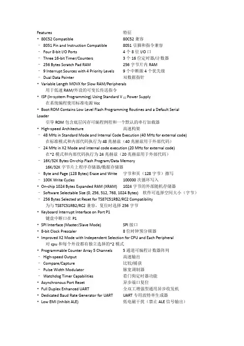
Features 特征•80C52 Compatible 80C52兼容–8051 Pin and Instruction Compatible 8051引脚和指令兼容–Four 8-bit I/O Ports 4个8位I/O口–Three 16-bit Timer/Counters 3个16位定时器/计数器–256 Bytes Scratch Pad RAM 256字节片内RAM–9 Interrupt Sources with 4 Priority Levels 9个中断源4个优先级–Dual Data Pointer 双数据指针•Variable Length MOVX for Slow RAM/Peripherals用于低速RAM/外设的可变长传送指令•ISP (In-system Programming) Using Standard V CC Power Supply在系统编程使用标准电源Vcc•Boot ROM Contains Low Level Flash Programming Routines and a Default Serial Loader引导ROM包含底层闪存可编程例程和一个默认的串行加载器•High-speed Architecture 高速构架–48 MHz in Standard Mode and Internal Code Execution (40 MHz for external code) 在标准模式和内部代码执行为48兆赫兹(40兆赫兹用于外部代码)–24 MHz in X2 Mode and internal code execution (20 MHz for external code) 在*2模式和内部代码执行为24兆赫兹(20兆赫兹用于外部代码)–16K/32K Bytes On-chip Flash Program/Data Memory16K/32K字节片上程序存储器/数据存储器–Byte and Page (128 Bytes) Erase and Write 字节和页(128字节)擦写–100K Write Cycles 100000次循环写入•On-chip 1024 Bytes Expanded RAM (XRAM) 1024字节的外部随机存储器–Software Selectable Size (0, 256, 512, 768, 1024 Bytes)软件可选择空间大小(字节)–256 Bytes Selected at Reset for TS87C51RB2/RC2 Compatibility为与TS87C51RB2/RC2兼容,复位时选择256字节•Keyboard Interrupt Interface on Port P1键盘中断口在P1•SPI Interface (Master/Slave Mode) SPI接口•8-bit Clock Prescaler 8位时钟预分频器•Improved X2 Mode with Independent Selection for CPU and Each Peripheral 对cpu和每个外设都有独立选择的*2模式•Programmable Counter Array 5 Channels 5通道可编程计数器阵列–High-speed Output 高速输出–Compare/Capture 比较/捕获–Pulse Width Modulator 脉宽调制器–Watchdog Timer Capabilities 看门狗定时器功能•Asynchronous Port Reset 异步端口复位•Full Duplex Enhanced UART 全双工增强型通用异步收发机•Dedicated Baud Rate Generator for UART UART专用波特率生成器•Low EMI (Inhibit ALE) 低电磁干扰(禁止ALE信号输出)•Hardware Watchdog Timer (One-time Enabled with Reset-out)硬件看门狗定时器•Power Control Modes 电压控制模式–Idle Mode 空闲模式–Power-down Mode 掉电模式–Power-off Flag 关机标志•Power Supply: 电源–2.7 to 3.6 (3V Version) 2.7-3.6(3V版本)–2.7 to 5.5V (5V Version) 2.7-5.5V(5V版本)•Temperature Ranges: Commercial (0 to +70°C) and Industrial (-40°C to +85°C) 温度范围:商业(0-70℃)工业(-40-85℃)•Packages: PDIL40, PLCC44, VQFP44 封装Description 描述The AT89C51RB2/RC2 is a high-performance(高性能)Flash version(版本)of the 80C51 8-bit micro-controllers(单片机). It contains a 16K or 32K Bytes Flash memory block(闪存块)for program and data.The Flash memory can be programmed either in parallel mode(并行方式)or in serial mode(串行方式)withthe ISP capability or with software(用isp或软件编程). The programming voltage is internally generated(内部产生)from the standard VCC pin.The AT89C51RB2/RC2 retains all features of the 80C52 with 256 Bytes of internalRAM, a 9-source AT89C51RB2/RC2保留80C52所有特性,256字节内部RAM,9个中断源4个控制级,三个定时器/计数器4-level interrupt controller and three timer/counters.In addition, the AT89C51RB2/RC2 has a Programmable Counter Array(计数器阵列), an XRAM of1024 Bytes, a Hardware Watchdog Timer, a Keyboard Interface,an SPI Interface(接口), amore versatile serial channel(通用串行通道)thatfacilitates multiprocessor communication (EUART多处理器通信)and a speedimprovement mechanism (X2 mode).The Pinout is the standard 40/44 pins of theC52. The fully static design reduces system power consumption of theAT89C51RB2/RC2 byallowing it to bring the clock frequency down to any value,even DC, without loss of data(全静态设计通过允许将时钟频率降低到任何值甚至直流来降低AT89C51RB2的功耗而又不丢失数据).The AT89C51RB2/RC2 has 2software-selectable(软件可选的)modes of reduced activity and 8-bitclockprescaler(预分频器) for further reduction in power consumption(为进一步降低功耗). In Idle(空闲)mode, the CPU is fro-zen(停止)while the peripherals(外设)and the interrupt system are still operating. In power-down(掉电)mode,the RAM is saved and all other functions are inoperative(不起作用).The addedfeatures of the AT89C51RB2/RC2 make it more powerful for applicationsthat needpulse width modulation(脉宽调制), high speed I/O and counting capabilities(计数功能)such asalarms, motor control(电机控制), corded phones(有线电话),and smart card readers(智能卡读卡器).。
AT89C51单片机实验开发板(使用说明-打印)
AT89C51单片机实验开发板使用手册 AT89C51单片机实验开发板是三门峡金聚宝单片机发展公司专为单片机初学者设计并开发的一种实验兼开发板,我们开发这个产品的目的就是为了帮助单片机初学者快速学会单片机技术。
在自学单片机的过程中,通过做了一系列的实验,可以比较容易地领会了单片机哪些枯燥、难懂的专业术语,而且这款实验开发板弥补了市场上常见的单片机实验板的一些不足,有针对性地面向最终的实用控制功能,增加了实用的继电器接口,可以使实验板能够直接用于控制各种负载,成为一个实用化的嵌入式控制系统。
目前想要学习单片机技术的网友可以分成两类,一类是业余的电子爱好者,想通过自学单片机来提高自己的电子技术水平,以后能够运用到自己熟悉的领域中有所作为,这类网友的动手能力比较好,但是理论知识一般欠缺一些。
另一类是在校的电子专业学生,为了完成一些科技项目或者是把学校学到的知识转化成实际的电子作品,为以后的工作求职创造更好的条件,这类网友需要的就是实践经验了。
我们也是从这两方面需求来开发这个产品的。
我们开设的单片机教程会以一个个独立的单元电路的形式,使单片机初学者在本手册的详细操作演示的指导下,一步一步通过自己安装元件、调试电路,将我们提供的多个实验按照从简单到复杂,从实现基本功能到完成扩展功能一步一步地完成,脚踏实地全面提高理论知识和动手能力。
以套件的形式提供还有一个好处,就是给后续开发创造空间,比如以后需要设计完成一个独特的单片机控制系统时,可以直接利用实验开发板的一些硬件资源,只安装上需要的元件,把精力集中在编写软件,就能快速完成项目。
本手册后附有我们的单片机实验开发板理图,供安装或实验时分析硬件结构。
教程构思:为了配合实验开发板的销售和使用,我们专门编写了一系列的实验教程,所有实验都按照从最简单到复杂原则,通过逐步的安装→实验→再安装→再实验的方式,最终完成所有实验。
我们提供所有实验的详细源程序,所有的程序都有详细的程序注释,而且都经过烧录验证的*.hex烧写文件。
AT89C51单片机中文资料

AT89C51单片机中文资料AT89C51是一种带4K字节闪烁可编程可擦除只读存储器(FPEROM—Falsh Programmable and Erasable Read Only Memory)的低电压,高性能CMOS8位微处理器,俗称单片机。
2.管脚说明:VCC:供电电压.GND:接地。
P0口:P0口为一个8位漏级开路双向I/O口,每脚可吸收8TTL门电流。
当P1口的管脚第一次写1时,被定义为高阻输入。
P0能够用于外部程序数据存储器,它可以被定义为数据/地址的第八位。
在FIASH编程时,P0 口作为原码输入口,当FIASH进行校验时,P0输出原码,此时P0外部必须被拉高。
P1口:P1口是一个内部提供上拉电阻的8位双向I/O口,P1口缓冲器能接收输出4TTL门电流。
P1口管脚写入1后,被内部上拉为高,可用作输入,P1口被外部下拉为低电平时,将输出电流,这是由于内部上拉的缘故。
在FLASH编程和校验时,P1口作为第八位地址接收。
P2口:P2口为一个内部上拉电阻的8位双向I/O口,P2口缓冲器可接收,输出4个TTL门电流,当P2口被写“1"时,其管脚被内部上拉电阻拉高,且作为输入。
并因此作为输入时,P2口的管脚被外部拉低,将输出电流。
这是由于内部上拉的缘故。
P2口当用于外部程序存储器或16位地址外部数据存储器进行存取时,P2口输出地址的高八位。
在给出地址“1”时,它利用内部上拉优势,当对外部八位地址数据存储器进行读写时,P2口输出其特殊功能寄存器的内容.P2口在FLASH编程和校验时接收高八位地址信号和控制信号。
P3口:P3口管脚是8个带内部上拉电阻的双向I/O口,可接收输出4个TTL门电流。
当P3口写入“1”后,它们被内部上拉为高电平,并用作输入。
作为输入,由于外部下拉为低电平,P3口将输出电流(ILL)这是由于上拉的缘故。
P3口也可作为AT89C51的一些特殊功能口,如下表所示:口管脚备选功能P3.0 RXD(串行输入口)P3.1 TXD(串行输出口)P3.2 /INT0(外部中断0)P3.3 /INT1(外部中断1)P3.4 T0(记时器0外部输入)P3.5 T1(记时器1外部输入)P3.6 /WR(外部数据存储器写选通)P3。
AT89C5131A_08资料
Features•Protocol–USB Used as Physical Layer–Device Firmware Upgrade Class Compliant–USB Clock Auto-Configuration•In-System Programming–Read/Write Flash and EEPROM Memories–Read Device ID–Full-chip Erase–Read/Write Configuration Bytes–Security Setting from ISP Command–Remote Application Start Command•In-Application Programming/Self Programming (IAP)–Read/Write Flash and EEPROM Memories–Read Device ID–Block Erase–Read/Write Configuration Bytes–Bootloader StartDescriptionThis document describes the USB bootloader functionalities as well as the USB proto-col to efficiently perform operations on the on-chip Flash (EEPROM) memories. Additional information on the AT89C5131A product can be found in the AT89C5131A datasheet and the AT89C5131A errata sheet available on the Atmel web site.The bootloader software package (binary) currently used for production is available from the Atmel web site.Bootloader Revision Purpose of Modifications DateRevision 1.0.2 First release25/03/2003 Revision 1.2.0Bootloader improvement20/03/200724287E–USB–04/08AT89C5131A USB BootloaderFunctional DescriptionThe AT89C5131A bootloader facilitates In-System Programming and In-Application Programming.In-System Programming Capability (IAP)In-System Programming allows the user to program or reprogram a microcontroller on-chip Flash memory without removing it from the system and without the need of a pre-programmed application.The USB bootloader can manage a communication with a host through the USB bus. It can also access and perform requested operations on the on-chip Flash memory.In-Application Programming or Self Programming Capability (ISP)In-Application Programming (IAP) allows the reprogramming of a microcontroller on-chip Flash memory without removing it from the system and while the embedded application is running.The USB bootloader contains some Application Programming Interface routines named API rou-tines that allow IAP by using the user’s firmware.Block DiagramThis section describes the different parts of the bootloader. Figure 1 shows the on-chip boot-loader and IAP processes.Figure 1. Bootloader Process DescriptionISP CommunicationManagementUser ApplicationUSB Protocol CommunicationManagementFlash MemoryExternal Host Via theFlash Memory IAP ManagementUser Call On-chip34287E–USB–04/08AT89C5131A USB BootloaderISP Communication ManagementThe purpose of this process is to manage the communication and its protocol between the on-chip bootloader and an external device (host). The on-chip bootloader implements a USB proto-col (see section “Protocol”). This process translates serial communication frames (USB) into Flash memory accesses (read, write, erase...).User Call Management Several Application Program Interface (API) calls are available to the application program toselectively erase and program Flash pages. All calls are made through a common interface (API calls) included in the bootloader. The purpose of this process is to translate the application request into internal Flash memory operations.Flash Memory ManagementThis process manages low level access to the Flash memory (performs read and write access).Bootloader ConfigurationConfiguration and Manufacturer InformationThe table below lists Configuration and Manufacturer byte information used by the bootloader.This information can be accessed through a set of API or ISP commands.Mnemonic Description Default ValueBSB Boot Status Byte FFh SBV Software Boot Vector FCh SSB Software Security Byte FFh EB Extra ByteFFh P1_CF Port 1 Configuration FEh P3_CF Port 3 Configuration FFh P4_CF Port 4 ConfigurationFFh Manufacturer 58h Id1: Family code D7h Id2: Product Name F7h Id3: Product RevisionDFh44287E–USB–04/08AT89C5131A USB BootloaderMapping and Default Value of Hardware Security Byte The 4 MSB of the Hardware Byte can be read/written by software (this area is called Fuse bits).The 4 LSB can only be read by software and written by hardware in parallel mode (with parallel programmer devices).Note:U: Unprogrammed = 1P: Program = 0SecurityThe bootloader has Software Security Byte (SSB) to protect itself from user access or ISP access.The Software Security Byte (SSB) protects from ISP accesses. The command "Program Soft-ware Security Bit" can only write a higher priority level. There are three levels of security:•Level 0: NO_SECURITY (FFh)This is the default level.From level 0, one can write level 1 or level 2.•Level 1: WRITE_SECURITY (FEh)In this level it is impossible to write in the Flash memory.The Bootloader returns an err_WRITE status.From level 1, one can write only level 2.•Level 2: RD_WR_SECURITY (FCh)Level 2 forbids all read and write accesses to/from the Flash memory.The Bootloader returns an err_WRITE or an err_VENDOR status.Only a full chip erase command can reset the software security bits.Bit PositionMnemonicDefault ValueDescription 7X2B U To start in x1 mode6BLJB P To map the boot area in code area between F800h-FFFFh 5OSCON1U Oscillator control (bit 1)4OSCON0U Oscillator control (bit 0)3reserved U 2LB2P To lock the chip (see datasheet)1LB1U 0LB0ULevel 0Level 1Level 2Flash/EEPROM Any access allowed Read only access allowed All access not allowed Fuse bitAny access allowed Read only access allowed All access not allowed BSB & SBV & EB Any access allowed Any access allowed Any access allowed SSBAny access allowed Write level2 allowed Read only access allowed Manufacturer info Read only access allowed Read only access allowed Read only access allowed Bootloader info Read only access allowed Read only access allowed Read only access allowed Erase block Allowed Not allowed Not allowed Full chip erase Allowed Allowed Allowed Blank CheckAllowedAllowedAllowed54287E–USB–04/08AT89C5131A USB BootloaderIn-System ProgrammingISP allows the user to program or reprogram a microcontroller’s on-chip Flash memory through the USB bus without removing it from the system and without the need of a pre-programmed application.This section describes how to start the USB bootloader and the higher level protocol over the USB.Boot ProcessThe bootloader can be activated in two ways: •Hardware conditions •Regular boot processFigure 3 and Figure 4 describe the boot process flows for low pin count and high pin count products.High Pin CountHardware ConditionsThe Hardware conditions (EA = 1, PSEN = 0) during the RESET rising edge force the on-chip bootloader execution. In this way the bootloader can be carried out regardless of the user Flash memory content. It is recommended to pull the PSEN pin down to ground though a 1K resistor to prevent the PSEN pin from being damaged (see Figure 2 below).Figure 2. ISP Hardware conditionsAs PSEN is an output port in normal operating mode (running user application or bootloader code) after reset, it is recommended to release PSEN after rising edge of reset signal. The hard-ware conditions are sampled at reset signal rising edge, thus they can be released at any time when reset input is high.Low Pin CountHardware ConditionsThe Hardware Condition forces the bootloader execution from reset.The default factory Hardware Condition is assigned to port P1.•P1 must be equal to FEhIn order to offer the best flexibility, the user can define its own Hardware Condition on one of the following Ports:•Port1ALEEAVCC/PSENRSTGND1K UnconnectedVCCVSS VCCGNDGND C1C2CrystalGND XTAL2XTAL1Bootloader64287E–USB–04/08AT89C5131A USB Bootloader•Port3•Port4 (only bit0 and bit1)The Hardware Condition configuration are stored in three bytes called P1_CF, P3_CF, P4_CF.These bytes can be modified by the user through a set of API or through an ISP command. There is a priority between P1_CF, P3_CF and P4_CF (see Figure 4 on page 9).Note:The BLJB must be at 0 (programmed) to be able to restart the bootloader.If the BLJB is equal to 1 (unprogrammed) only the hardware parallel programmer can change this bit (see AT89C5131A datasheet for more details).74287E–USB–04/08AT89C5131A USB BootloaderSoftware Boot VectorThe default value [FF]00h is used in ISP mode. The boot address is, in this mode, the lowest adress of FM1 USB bootloader.The Software Boot Vector (SBV) can be used to force the execution of a user bootloader starting at address [SBV]00h in the application area (FM0).The way to start this user bootloader is described in section “Boot Process”.FLIP Software ProgramFLIP is a PC software program running under Windows ® 9x/Me/2000/XP and Linux ® which can be used in ISP mode and which supports all Atmel C51 Flash microcontroller and USB protocol communication media.The FLIP software program is free and is available from the Atmel web site.USB BootloaderApplicationUser Bootloader[SBV]00hFM1FM0[FC]00h84287E–USB–04/08AT89C5131A USB Bootloader94287E–USB–04/08AT89C5131A USB BootloaderFigure 4. Low-pin Count Regular Boot Process104287E–USB–04/08AT89C5131A USB BootloaderPhysical LayerThe USB norm specifies all the transfers over the USB line. The USB specification also includes several CLASS and SUB-CLASS specifications. These stand-alone documents are used by the manufacturer to implement a USB link between a PC and a device supporting the In System Programming. Mostly, the USB specification is implemented by hardware (automatic reply,handshakes, timings, ...) and the USB Classes and SubClasses are implemented by software at a data level.Figure 5. USB Bus TopographyThe USB is used to transmit information that has the following configuration:•USB DFU using the Default Control Endpoint only (endpoint 0) with a 32 bytes length.•48 MHz for USB controller: USB clock configuration performed by the bootloader48 MHz Frequency Auto-Configuration The bootloader includes a function which will automatically setup the PLL frequency (48MHz)versus the different XTAL configuration used on the application.The table below shows the allowed frequencies compatible with the USB bootloader48 MHz auto-generation.PC (Host)Application (Device)USB LineDownstream Transfer: OUT Upstream Transfer: INPC DriverPC ApplicationDevice driver/API Firmware6 MHz8 MHz 12 MHz 16 MHz 20 MHz 24 MHz 32 MHz 40 MHz 48 MHz X1 or X2Clock ModesOKOKOKOKOKOKOKOKOK114287E–USB–04/08AT89C5131A USB BootloaderFigure 6. 48 MHz Frequency Auto-ConfigurationMAINUSB Connected?Suspend/ResumeConfigure PLL for Frequency X Configure Timer 0SOF Detected?Timer 0 Overflow?USB SchedulerChange FrequencyResume Detected?YesNoNoYesYesNoYesNo124287E–USB–04/08AT89C5131A USB BootloaderProtocolDevice Firmware Upgrade IntroductionDevice Firmware Upgrade is the mechanism for accomplishing the task of upgrading the device firmware. Any class of USB device can exploit this capability by supporting the requirements specified in this document.Because it is impractical for a device to concurrently perform both DFU operations and its nor-mal run-time activities, those normal activities must cease for the duration of the DFU operations. Doing so means that the device must change its operating mode; i.e., a printer is not a printer while it is undergoing a firmware upgrade; it is a PROM programmer. However, a device that supports DFU is not capable of changing its mode of operation on its own. External (human or host operating system) intervention is required.DFU Specific RequestsIn addition of the USB standard requests, 7 DFU class-specific requests are employed to accomplish the upgrade operations (Table 1):DFU Descriptors Set The device exports the DFU descriptor set, which contains:• A DFU device descriptor • A single configuration descriptor• A single interface descriptor (including descriptors for alternate settings, if present)•A single functional descriptorDFU Device DescriptorThis descriptor is only present in the DFU mode descriptor set. The DFU class code is reported in the bDeviceClass field of this descriptor.Table 2. USB ParametersTable 1. DFU Class-specific RequestsbmRequestType bRequest wValue wIndex wLength Data 0010 0001b DFU_DETACH (0)wTimeout Interface (4)Zero none 0010 0001b DFU_DNLOAD (1)wBlock Interface (4)Length Firmware 1010 0001b DFU_UPLOAD (2)wBlock Interface (4)Length Firmware 1010 0001b DFU_GETSTATUS (3)Zero Interface (4)6Status 0010 0001b DFU_CLRSTATUS (4)Zero Interface (4)Zero none 1010 0001b DFU_GETSTATE (5)Zero Interface (4)1State 0010 0001bDFU_ABORT (6)ZeroInterface (4)ZerononeParameter Atmel – AT89C5131A BootloaderVendor ID 0x03EB Product ID 0x2FFD Release Number0x0000134287E–USB–04/08AT89C5131A USB BootloaderTable 3. DFU Mode Device DescriptorDFU Configuration DescriptorThis descriptor is identical to the standard configuration descriptor described in the USB DFU specification version 1.0, with the exception that the bNumInterfaces field must contain the value 01h.DFU Interface DescriptorThis is the descriptor for the only interface available when operating in DFU mode. Therefore,the value of the bInterfaceNumber field is always zero.Table 4. DFU Mode Interface Descriptoreach alternate setting employ a string descriptor to indicate the target memory segment; e.g., “EEPROM”. Details concern-ing other possible uses of alternate settings are beyond the scope of this document. However, their use is intentionally not restricted because the authors anticipate that implementers will devise additional creative uses for alternate settings.Offset Field Size Value Description0bLength 112h Size of this descriptor, in bytes 1bDescriptorType101h DFU FUNCTIONAL descriptor type2bcdUSB 20100h USB specification release number in binary coded decimal 4bDeviceClass 1FEh Application Specific Class Code 5bDeviceSubClass 101h Device Firmware Upgrade Code6bDeviceProtocol 100h The device does not use a class specific protocol on this interface 7bMaxPacketSize0132Maximum packet size for endpoint zero 8idVendor 203EBh Vendor ID 10idProduct 22FFDh Product ID12bcdDevice 20x0000Device release number in binary coded decimal 14iManufacturer 10Index of string descriptor 15iProduct 10Index of string descriptor 16iSerialNumber 10Index of string descriptor 17bNumConfigurations101hOne configuration only for DFUOffset Field Size Value Description0bLength 109h Size of this descriptor, in bytes 1bDescriptorType 104h INTERFACE descriptor type 2bInterfaceNumber 100h Number of this interface 3bAlternateSetting 100h Alternate setting (1)4bNumEndpoints 100h Only the control pipe is used 5bInterfaceClass 1FEh Application Specific Class Code 6bInterfaceSubClass 101h Device Firmware Upgrade Code7bInterfaceProtocol100h The device doesn’t use a class specific protocol on this interface 8iInterface100hIndex of the String descriptor for this interface144287E–USB–04/08AT89C5131A USB BootloaderDFU Functional DescriptorTable 5. DFU Functional DescriptorCommand Description This protocol allows to:•Initiate the communication•Program the Flash or EEPROM Data •Read the Flash or EEPROM Data •Program Configuration Information•Read Configuration and Manufacturer Information •Erase the Flash •Start the applicationOverview of the protocol is detailed in Appendix-A.Offset Field Size Value Description0bLength 107h Size of this descriptor, in bytes 1bDescriptorType121hDFU FUNCTIONAL descriptor type 2bmAttributes 1Bit maskDFU Attributes:bit 7..3: reservedbit 2: device is able to communicate via USB after Manifestation phase 1 = yes, 0 = no, must see bus resetbit 1: bitCanUpload : upload capable 1 = yes, 0 = no bit 0: bitCanDnload : download capable 1 = yes, 0 = no 3wDetachTimeOut 2NumberTime in milliseconds that the device will wait after receipt of the DFU_DETACH request.If this time elapses without a USB reset, the device will terminate the Reconfiguration phase and revert back to normal operation. This represents the maximum time that the device can wait (depending on its timers, ...). The Host may specify a shorter timeout in the DFU_DETACH request.5wTransferSize 2NumberMaximum number of bytes that the device can accept per control-write transaction154287E–USB–04/08AT89C5131A USB BootloaderDevice StatusGet StatusThe Host employs the DFU_GETSTATUS request to facilitate synchronization with the device.This status gives information on the execution of the previous request: in progress/OK/Fail/...The device responds to the DFU_GETSTATUS request with a payload packet containing the fol-lowing data:Table 6. DFU_GETSTATUS ResponsebmRequestType bRequest wValue wIndex wLengthData 1010 0001b DFU_GETSTATUS (3)Zero Interface (4)6Status 0010 0001bDFU_CLRSTATUS (4)ZeroInterface (4)ZerononeOffset Field Size Value DescriptionbStatus1Numb erAn indication of the status resulting from the execution of the most recent request.1bwPollTimeOut 3Numb erMinimum time in milliseconds that the host should wait before sending a subsequentDFU_GETSTATUS. The purpose of this field is to allow the device to dynamically adjust theamount of time that the device expects the host to wait between the status phase of the next DFU_DNLOAD and the subsequent solicitation of the device’s status via DFU_GETSTATUS.4bState 1Numb er An indication of the state that the device is going to enter immediately following transmission of this response.5iString1IndexIndex of status description in string table.Table 7. bStatus valuesStatus Value DescriptionOK 0x00No error condition is presenterrTARGET 0x01File is not targeted for use by this deviceerrFILE 0x02File is for this device but fails some vendor-specific verification test errWRITE 0x03Device id unable to write memory errERASE0x04Memory erase function failed errCHECK_ERASED 0x05Memory erase check failed errPROG 0x06Program memory function failed errVERIFY 0x07Programmed memory failed verificationerrADDRESS 0x08Cannot program memory due to received address that is out of rangeerrNOTDONE 0x09Received DFU_DNLOAD with wLength = 0, but device does not think it has all the data yet.errFIRMWARE 0x0A Device’s firmware is corrupted. It cannot return to run-time operationserrVENDOR0x0BiString indicates a vendor-specific error164287E–USB–04/08AT89C5131A USB BootloaderTable 8. bState ValuesClear StatusAny time the device detects an error and reports an error indication status to the host in the response to a DFU_GETSTATUS request, it enters the dfuERROR state. The device cannot transition from the dfuERROR state, after reporting any error status, until after it has received a DFU_CLRSTATUS request. Upon receipt of DFU_CLRSTATUS, the device sets a status of OK and transitions to the dfuIDLE state. Only then is it able to transition to other states.errUSBR 0x0C Device detected unexpected USB reset signaling errPOR 0x0D Device detected unexpected power on reseterrUNKNOWN 0x0E Something went wrong, but the device does not know what it was errSTALLEDPK0x0FDevice stalled an unexpected requestTable 7. bStatus values (Continued)Status Value DescriptionState Value DescriptionappIDLE 0Device is running its normal applicationappDETACH 1Device is running its normal application, has received the DFU_DETACH request, and is waiting for a USB resetdfuIDLE2Device is operating in the DFU mode and is waiting for requests dfuDNLOAD-SYNC 3Device has received a block and is waiting for the Host to solicit the status via DFU_GETSTATUSdfuDNBUSY 4Device is programming a control-write block into its non volatile memories dfuDNLOAD-IDLE5Device is processing a download operation. Expecting DFU_DNLOAD requestsdfuMANIFEST-SYNC 6Device has received the final block of firmware from the Host and iswaiting for receipt of DFU_GETSTATUS to begin the Manifestation phaseordevice has completed the Manifestation phase and is waiting for receipt of DFU_GETSTATUS.dfuMANIFEST 7Device is in the Manifestation phase.dfuMANIFEST-WAIT-RESET8Device has programmed its memories and is waiting for a USB reset or a power on reset.dfuUPLOAD-IDLE 9The device is processing an upload operation. Expecting DFU_UPLOAD requests.dfuERROR10An error has occurred. Awaiting the DFU_CLRSTATUS request.bmRequestType bRequest wValue wIndex wLengthData 0010 0001bDFU_CLRSTATUS (4)ZeroInterface (4)None174287E–USB–04/08AT89C5131A USB BootloaderDevice StateThis request solicits a report about the state of the device. The state reported is the current state of the device with no change in state upon transmission of the response. The values specified in the bState field are identical to those reported in DFU_GETSTATUS.DFU_ABORT requestThe DFU_ABORT request enables the device to exit from certain states and return to the DFU_IDLE state. The device sets the OK status on receipt of this request. For more information,see the corresponding state transition summary.Programming the Flash or EEPROM DataThe firmware image is downloaded via control-write transfers initiated by the DFU_DNLOAD class-specific request. The host sends between bMaxPacketSize0 and wTransferSize bytes to the device in a control-write transfer. Following each downloaded block, the host solicits the device status with the DFU_GETSTATUS request.As described in the USB DFU Specification, "Firmware images for specific devices are, by defi-nition, vendor specific. It is therefore required that target addresses, record sizes, and all other information relative to supporting an upgrade are encapsulated within the firmware image file. It is the responsibility of the device manufacturer and the firmware developer to ensure that their devices can consume these encapsulated data. With the exception of the DFU file suffix, the content of the firmware image file is irrelevant to the host."Firmware image:•32 bytes: Command•X bytes: X is the number of byte (00h) added before the first significative byte of thefirmware. The X number is calculated to align the beginning of the firmware with the flash page. X = start_address [32]. For example, if the start address is 00AFh (175d), X = 175 [32] = 15.•The firmware•The DFU Suffix on 16 Bytes.Table 9. DFU File SuffixbmRequestType bRequest wValue wIndex wLengthData 1010 0001bDFU_GETSTATE (5)ZeroInterface (4)1StatebmRequestType bRequest wValue wIndex wLengthData 1010 0001bDFU_ABORT (6)ZeroInterface (4)NoneOffset Field Size Value Description-0dwCRC 4Number The CRC of the entire file, excluding dwCRC -4bLength116The length of this DFU suffix including dwCRC-5ucDfuSignature 3 5 : 44h6 : 46h7 : 55hThe unique DFU signature field-8bcdDFU 2BCD 0100h DFU specification number-10idVendor 2IDThe vendor ID associated with this file. Either FFFFh or must match device’s vendor ID184287E–USB–04/08AT89C5131A USB BootloaderRequest From HostWrite CommandThe write command is 6 bytes long. In order to reach the USB specification of the Control type transfers, the write command is completed with 26 (= 32 - 6) non-significant bytes. The total length of the command is then 32 bytes, which is the length of the Default Control Endpoint.FirmwareThe firmware can now be downloaded to the device. In order to be in accordance with the Flash page size (128 bytes), X non-significant bytes are added before the first byte to program. The X number is calculated to align the beginning of the firmware with the Flash page. X =start_address [32]. For example, if the start address is 00AFh (175d), X = 175 [32] = 15.DFU SuffixThe DFU suffix of 16 bytes are added just after the last byte to program. This suffix is reserved for future use.-12idProduct2IDThe product ID associated with this file. Either FFFFf or must match the device’s product ID-14bcdDevice 2BCDThe release number of the device associated with this file. Either FFFFh or a BCD firmware release or version numberOffset Field Size Value DescriptionbmRequestType bRequest wValue wIndex wLength Data 0010 0001bDFU_DNLOAD (1)wBlockInterface (4)LengthFirmwareCommand Identifier data[0]data[1]data[2]data[3]data[4]Description Id_prog_start01h00hstart_addressend_addressInit FLASH programming01hInit EEPROM programming194287E–USB–04/08AT89C5131A USB BootloaderFigure 7. Example of Firmware Download Zero Length DFU_DNLOAD RequestThe Host sends a DFU_DNLOAD request with the wLength field cleared to 0 to the device to indicate that it has completed transferring the firmware image file. This is the final payload packet of a download operation.This operation should be preceded by a Long Jump address specification using the correspond-ing Flash command.Answers from BootloaderAfter each program request, the Host can request the device state and status by sending a DFU_GETSTATUS message.If the device status indicates an error, the host can send a DFU_CLRSTATUS request to the device.OUT Prog_Start + (EP0 fifo length - 6) x 00h SETUP DFU_DNLOADOUT X offset bytes + Firmware Packet 1OUTFirmware Packet 2OUT Firmware Packet n + DFU suffix INZLP204287E–USB–04/08AT89C5131A USB BootloaderReading the Flash or EEPROM DataThe flow described below allows the user to read data in the Flash memory or in the EEPROMdata memory. A blank check command on the Flash memory is possible with this flow.This operation is performed in 2 steps:1.DFU_DNLOAD request with the read command (6 bytes)2.DFU_UPLOAD request which correspond to the immediate previous command.First Request from Host The Host sends a DFU Download request with a Display command in the data field.Second Request from HostThe Host sends a DFU Upload request.Answers from the DeviceThe device send to the Host the firmware from the specified start address to the end address.CommandIdentifierdata[0]data[1]data[2]data[3]data[4]Description Id_display_data03h00hstart_address end_address Display FLASH Data01h Blank Check in FLASH 02hDisplay EEPROM DataOUT Display_Data (6 bytes)SETUP DFU_DNLOAD INZLPIN Firmware Packet 1INFirmware Packet 2IN Firmware Packet n OUTZLPSETUP DFU_UPLOAD214287E–USB–04/08AT89C5131A USB BootloaderAnswers from the Device to a Blank Check Command The Host controller send a GET_STATUS request to the device. Once internal blank check has been completed, the device sends its status.•If the device status is “OK”:the device memory is then blank and the device waits the next Host request.•If the device status is “errCHECK_ERASED”:the device memory is not blank. The device waits for an DFU_UPLOAD request to send the first address where the byte is not 0xFF.Programming Configuration InformationThe flow described below allows the user to program Configuration Information regarding the bootloader functionality.•Boot Process Configuration:–BSB –SBV–P1_CF, P3_CF and P4_CF–Fuse bits (BLJB, X2 and OSCON bits) (see section “Mapping and Default Value of Hardware Security Byte”)Take care that the Program Fuse bit command programs the 4 Fuse bits at the same time.Request from HostTo start the programming operation, the Host sends DFU_DNLOAD request with the Write com-mand in the data field (6 bytes).Answers From BootloaderThe device has two possible answers to a DFU_GETSTATUS request:•If the chip is protected from program access, a “err_WRITE” status is returned to the Host.•Otherwise, the device status is “OK“.Command Identifierdata[0]data[1]data[2]data[3]data[4]Description Id_write_command04h01h 00h Value Write value in BSB 01h Write value in SBV 02hWrite P1_CF03h Write P3_CF 04h Write P4_CF 05h Write value in SSB 06hWrite value in EB02h 00h ValueWrite value in Fuse (HSB)OUT Write_command (6 bytes)SETUP DFU_DNLOAD INZLP。
AT89C51单片机说明
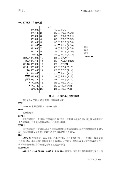
PSEN 此为"Program Store Enable"的缩写。访问外部程序存储器选通信号,低电平有效。在访
(60KB)
0FFFFH
1000H
外部 程序 存储器
0FFFH
EA=0 (4KB)
0000H
0FFFFH
外 部 数 据 存 储 器
(64KB)
0000H
图 2-2 只读程序存储器
图 2-3 外部数据存储器
直接地址
2FH 7F 7E 7D 7C 7B 7A 79 78 2EH 77 76 75 74 73 72 71 70 2DH 6F 6E 6D 6C 6B 6A 69 68 2CH 67 66 65 64 63 62 61 60 2BH 5F 5E 5D 5C 5B 5A 59 58 2AH 57 56 55 54 53 52 51 50 29H 4F 4E 4D 4C 4B 4A 49 48 28H 47 46 45 44 43 42 41 40 位寻址区 27H 3F 3E 3D 3B 3C 3A 39 38 26H 37 36 35 34 33 32 31 30 25H 2F 2E 2D 2B 2C 2A 29 28 24H 27 26 25 24 23 22 21 20 23H 1F 1E 1D 1C 1B 1A 19 18 22H 17 16 15 14 13 12 11 10 21H 0F 0E 0D 0C 0B 0A 09 08 20H 07 06 05 04 03 02 01 00 1FH
at89c5131手册翻译
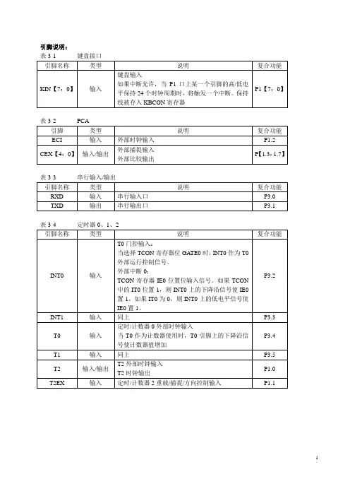
引脚说明:表3-1 键盘接口表3-2 PCA表3-3 串行输入/输出表3-4 定时器0、1、2表3-5 LED表3-6 I2表3-7 SPI表3-8 端口表3-10 USB表3-11 系统表3-12 电源6. SFR映象AT89C5130A/31A-M特殊功能寄存器(SFR)的可分为以下类别:• C51 内核寄存器::ACC、B、DPH、DPL、PSW、SP• I/O 端口寄存器:P0、P1、P2、P3、P4• 定时寄存器::T2CON、T2MOD、TCON、TH0、TH1、TH2、TMOD、TL0、TL1、TL2、RCAP2L、RCAP2H• 串行I/O端口(Serial I/O port)寄存器:SADDR、SADEN、SBUF、SCON• PCA (Programmable Counter Array) 寄存器:CCON, CMOD, CCAPMx, CL, CH, CCAPxH,CCAPxL (x: 0 to 4)• 电源时钟控制(Power and clock control)寄存器:PCON• 硬件WDT(Hardware Watchdog Timer)寄存器:WDTRST、WDTPRG•中断控制:IEN0、IPL0、IPH0、IEN1、IPL1、IPH1• 键盘接口寄存器:(Keyboard Interface)寄存器:KBE、KBF、KBLS• LED 寄存器:LEDCON• I2C(Two Wire Interface )寄存器:SSCON、SSCS、SSDAT、SSADR• Serial Port Interface (SPI) 寄存器:SPCON、SPSTA、SPDAT• USB寄存器:Uxxx (17 registers)• PLL 寄存器:PLLCON、PLLDIV• BRG (Baud R ate Generator) 寄存器:BRL、BDRCON• Flash 寄存器:FCON (FCON access is reserved for the Flash API and ISP software)• EEPROM 寄存器:EECON• 其他寄存器:AUXR、AUXR1、CKCON0、CKCON1SFR地址分配表双数据指针:1、AUXR1寄存器:辅助寄存器(#0A2H)PCA模块:1、CMOD寄存器:PCA控制方式寄存器(D9h)2、CCON寄存器:PCA计数器控制寄存器(D8h)串口通信:中断系统4、IEN1寄存器(B1h)6、IPH1寄存器(B3h)SPITWIUSB3、USBIEN寄存器(S:BEh)6、UEPCONX寄存器(S:D4h)9、UBYCTLX寄存器(S:E2h)11、UEPRST寄存器(S:D5h)14、UFNUMH寄存器(S:BBh,只读)PCAPCA提供了更多的定时功能,同时比起标准的定时/计数器,CPU的介入更少。
AT89C51RC-24JC资料
1Features•Compatible with MCS-51® Products•32K Bytes of Reprogrammable Flash Memory •Endurance: 1000 Write/Erase Cycles •4V to 5.5V Operating Range•Fully Static Operation: 0 Hz to 33 MHz •Three-level Program Memory Lock •512 x 8-bit Internal RAM •32 Programmable I/O Lines •Three 16-bit Timer/Counters •Eight Interrupt Sources•Programmable Serial Channel•Low-power Idle and Power-down Modes •Interrupt Recovery from Power-down Mode •Hardware Watchdog Timer •Dual Data Pointer •Power-off FlagDescriptionThe AT89C51RC is a low-power, high-performance CMOS 8-bit microcontroller with 32K bytes of Flash programmable read only memory and 512 bytes of RAM. The device is manufactured using Atmel’s high-density nonvolatile memory technology and is compatible with the industry-standard 80C51 and 80C52 instruction set and pinout.The on-chip Flash allows the program memory to be user programmed by a conven-tional nonvolatile memory programmer. A total of 512 bytes of internal RAM are available in the AT89C51RC. The 256-byte expanded internal RAM is accessed via MOVX instructions after clearing bit 1 in the SFR located at address 8EH. The other 256-byte RAM segment is accessed the same way as the Atmel AT89-series and other 8052-compatible products. By combining a versatile 8-bit CPU with Flash on a monolithic chip, the Atmel AT89C51RC is a powerful microcomputer which provides a highly-flexible and cost-effective solution to many embedded control applications.The AT89C51RC provides the following standard features: 32K bytes of Flash, 512bytes of RAM, 32 I/O lines, three 16-bit timer/counters, a six-vector two-level interrupt architecture, a full duplex serial port, on-chip oscillator, and clock circuitry. In addition,the A T89C51RC is designed with static logic for operation down to zero frequency and supports two software selectable power saving modes. The Idle Mode stops the CPU while allowing the RAM, timer/counters, serial port, and interrupt system to continue functioning. The Power-down mode saves the RAM contents but freezes the oscillator,disabling all other chip functions until the next external interrupt or hardware reset.2AT89C51RC1920B–MICRO–11/02Pin ConfigurationsTQFPPDIPPLCC3AT89C51RC1920B–MICRO–11/02Block Diagram4AT89C51RC1920B–MICRO–11/02Pin DescriptionVCC Supply voltage.GND Ground.Port 0Port 0 is an 8-bit open drain bidirectional I/O port. As an output port, each pin can sink eight TTL inputs. When 1s are written to port 0 pins, the pins can be used as high-impedance inputs.Port 0 can also be configured to be the multiplexed low-order address/data bus during accesses to external program and data memory. In this mode, P0 has internal pull-ups.Port 0 also receives the code bytes during Flash programming and outputs the code bytes during program verification. External pull-ups are required during program verification.Port 1Port 1 is an 8-bit bidirectional I/O port with internal pull-ups. The Port 1 output buffers can sink/source four TTL inputs. When 1s are written to Port 1 pins, they are pulled high by the internal pull-ups and can be used as inputs. As inputs, Port 1 pins that are exter-nally being pulled low will source current (I IL ) because of the internal pull-ups.In addition, P1.0 and P1.1 can be configured to be the timer/counter 2 external count input (P1.0/T2) and the timer/counter 2 trigger input (P1.1/T2EX), respectively, as shown in the following table.Port 1 also receives the low-order address bytes during Flash programming and verification.Port 2Port 2 is an 8-bit bidirectional I/O port with internal pull-ups. The Port 2 output buffers can sink/source four TTL inputs. When 1s are written to Port 2 pins, they are pulled high by the internal pull-ups and can be used as inputs. As inputs, Port 2 pins that are exter-nally being pulled low will source current (I IL ) because of the internal pull-ups.Port 2 emits the high-order address byte during fetches from external program memory and during accesses to external data memory that use 16-bit addresses (MOVX @DPTR). In this application, Port 2 uses strong internal pull-ups when emitting 1s. During accesses to external data memory that use 8-bit addresses (MOVX @ RI), Port 2 emits the contents of the P2 Special Function Register.Port 2 also receives the high-order address bits and some control signals during Flash programming and verification.Port 3Port 3 is an 8-bit bidirectional I/O port with internal pull-ups. The Port 3 output buffers can sink/source four TTL inputs. When 1s are written to Port 3 pins, they are pulled high by the internal pull-ups and can be used as inputs. As inputs, Port 3 pins that are exter-nally being pulled low will source current (I IL ) because of the pull-ups.Port 3 receives some control signals for Flash programming and verification.Port 3 also serves the functions of various special features of the AT89C51RC, as shown in the following table.Port Pin Alternate FunctionsP1.0T2 (external count input to Timer/Counter 2), clock-outP1.1T2EX (Timer/Counter 2 capture/reload trigger and direction control)5AT89C51RC1920B–MICRO–11/02RSTReset input. A high on this pin for two machine cycles while the oscillator is running resets the device. This pin drives High for 98 oscillator periods after the Watchdog times out. The DISRTO bit in SFR AUXR (address 8EH) can be used to disable this feature. In the default state of bit DISRTO, the RESET HIGH out feature is enabled.Address Latch Enable is an output pulse for latching the low byte of the address during Flash programming.In normal operation, ALE is emitted at a constant rate of 1/6 the oscillator frequency and may be used for external timing or clocking purposes. Note, however, that one ALE pulse is skipped during each access to external data memory.If desired, ALE operation can be disabled by setting bit 0 of SFR location 8EH. With the bit set, ALE is active only during a MOVX or MOVC instruction. Otherwise, the pin is weakly pulled high. Setting the ALE-disable bit has no effect if the microcontroller is in external execution mode.Program Store Enable is the read strobe to external program memory.each access to external data memory.fetch code from external program memory locations starting at 0000H up to for internal program executions.This pin also receives the 12-volt programming enable voltage (V PP ) during Flash programming.XTAL1Input to the inverting oscillator amplifier and input to the internal clock operating circuit.XTAL2Output from the inverting oscillator amplifier.Port Pin Alternate Functions P3.0RXD (serial input port)P3.1TXD (serial output port)P3.2INT0 (external interrupt 0)P3.3INT1 (external interrupt 1)P3.4T0 (timer 0 external input)P3.5T1 (timer 1 external input)P3.6WR (external data memory write strobe)P3.7RD (external data memory read strobe)6AT89C51RC1920B–MICRO–11/02Table 1. AT89C51RC SFR Map and Reset Values0F8H 0FFH 0F0H B 000000000F7H 0E8H 0EFH 0E0H ACC 000000000E7H 0D8H 0DFH 0D0H PSW 000000000D7H 0C8H T2CON 00000000T2MOD XXXXXX00RCAP2L 00000000RCAP2H 00000000TL200000000TH2000000000CFH 0C0H 0C7H 0B8H IP XX0000000BFH 0B0H P3111111110B7H 0A8H IE 0X0000000AFH 0A0H P211111111AUXR1XXXXXXX0WDTRST XXXXXXXX0A7H 98H SCON 00000000SBUF XXXXXXXX9FH 90H P11111111197H 88H TCON 00000000TMOD 00000000TL000000000TL100000000TH000000000TH100000000AUXR XXX00X008FH 80HP011111111SP 00000111DP0L 00000000DP0H 00000000DP1L 00000000DP1H 00000000PCON 0XXX000087H7AT89C51RC1920B–MICRO–11/02Special Function RegistersA map of the on-chip memory area called the Special Function Register (SFR) space is shown in Table 1.Note that not all of the addresses are occupied, and unoccupied addresses may not be implemented on the chip. Read accesses to these addresses will in general return ran-dom data, and write accesses will have an indeterminate effect.User software should not write 1s to these unlisted locations, since they may be used in future products to invoke new features. In that case, the reset or inactive values of the new bits will always be 0.Timer 2 Registers: Control and status bits are contained in registers T2CON (shown in Table 2) and T2MOD (shown in Table 3) for Timer 2. The register pair (RCAP2H,RCAP2L) are the Capture/Reload registers for Timer 2 in 16-bit capture mode or 16-bit auto-reload mode.Interrupt Registers: The individual interrupt enable bits are in the IE register. Two pri-orities can be set for each of the six interrupt sources in the IP register.Table 2. T2CON – Timer/Counter 2 Control RegisterT2CON Address = 0C8H Reset Value = 0000 0000BBit Addressable BitTF2EXF2RCLK TCLK EXEN2TR2C/T2CP/RL27654321Symbol FunctionTF2Timer 2 overflow flag set by a Timer 2 overflow and must be cleared by software. TF2 will not be set when either RCLK = 1 or TCLK = 1.EXF2Timer 2 external flag set when either a capture or reload is caused by a negative transition on T2EX and EXEN2 = 1. When Timer 2 interrupt is enabled, EXF2 = 1 will cause the CPU to vector to the Timer 2 interrupt routine. EXF2 must be cleared by software. EXF2 does not cause an interrupt in up/down counter mode (DCEN = 1).RCLK Receive clock enable. When set, causes the serial port to use Timer 2 overflow pulses for its receive clock in serial port Modes 1 and 3. RCLK = 0 causes Timer 1 overflow to be used for the receive clock.TCLK Transmit clock enable. When set, causes the serial port to use Timer 2 overflow pulses for its transmit clock in serial port Modes 1 and 3. TCLK = 0 causes Timer 1 overflows to be used for the transmit clock.EXEN2Timer 2 external enable. When set, allows a capture or reload to occur as a result of a negative transition on T2EX if Timer 2 is not being used to clock the serial port. EXEN2 = 0 causes Timer 2 to ignore events at T2EX.TR2Start/Stop control for Timer 2. TR2 = 1 starts the timer.C/T2Timer or counter select for Timer 2. C/T2 = 0 for timer function. C/T2 = 1 for external event counter (falling edge triggered).CP/RL2Capture/Reload select. CP/RL2 = 1 causes captures to occur on negative transitions at T2EX if EXEN2 = 1. CP/RL2 = 0 causes automatic reloads to occur when Timer 2 overflows or negative transitions occur at T2EX when EXEN2 = 1. When either RCLK or TCLK = 1, this bit is ignored and the timer is forced to auto-reload on Timer 2 overflow.8AT89C51RC1920B–MICRO–11/02Dual Data Pointer Registers: To facilitate accessing both internal and external data memory, two banks of 16-bit Data Pointer Registers are provided: DP0 at SFR address locations 82H-83H and DP1 at 84H-85H. Bit DPS = 0 in SFR AUXR1 selects DP0 and DPS = 1 selects DP1. The user should always initialize the DPS bit to the appropriate value before accessing the respective Data Pointer Register.Power Off Flag: The Power Off Flag (POF) is located at bit 4 (PCON.4) in the PCON SFR. POF is set to “1” during power up. It can be set and rest under software control and is not affected by reset.Table 3a. AUXR: Auxiliary RegisterAUXRAddress = 8EH Reset Value = XXX00X00BNot Bit Addressable–––WDIDLEDISRTO–EXTRAMDISALEBit7654321–Reserved for future expansion DISALEDisable/Enable ALE DISALE Operating Mode0ALE is emitted at a constant rate of 1/6 the oscillator frequency 1ALE is active only during a MOVX or MOVC instructionEXTRAM Internal/External RAM access using MOVX @ Ri/@DPTR EXTRAM Operating Mode0Internal ERAM (00H-FFH) access using MOVX @ Ri/@DPTR 1External data memory accessDISRTO Disable/Enable Reset out DISRTO Operating Mode0Reset pin is driven High after WDT times out 1Reset pin is input onlyWDIDLE Disable/Enable WDT in IDLE mode WDIDLE Operating Mode0WDT continues to count in IDLE mode 1WDT halts counting in IDLE mode9AT89C51RC1920B–MICRO–11/02Memory Organization MCS-51 devices have a separate address space for Program and Data Memory. Up to 64K bytes each of external Program and Data Memory can be addressed.Program MemoryCC , program fetches to addresses 0000H through 7FFFH are directed to internal memory and fetches to addresses 8000H through FFFFH are to external memory.Data MemoryThe AT89C51RC has internal data memory that is mapped into four separate segments:the lower 128 bytes of RAM, upper 128 bytes of RAM, 128 bytes special function regis-ter (SFR) and 256 bytes expanded RAM (ERAM).The four segments are:1.The Lower 128 bytes of RAM (addresses 00H to 7FH) are directly and indirectlyaddressable.2.The Upper 128 bytes of RAM (addresses 80H to FFH) are indirectly addressableonly.3.The Special Function Registers, SFRs, (addresses 80H to FFH) are directlyaddressable only.4.The 256-byte expanded RAM (ERAM, 00H-FFH) is indirectly accessed by MOVXinstructions, and with the EXTRAM bit cleared.The Lower 128 bytes can be accessed by either direct or indirect addressing. The Upper 128 bytes can be accessed by indirect addressing only. The Upper 128 bytes occupy the same address space as the SFR. This means they have the same address, but are physically separate from the SFR space.When an instruction accesses an internal location above address 7FH, the CPU knows whether the access is to the upper 128 bytes of data RAM or to SFR space by the addressing mode used in the instruction. Instructions that use direct addressing access SFR space. For example:MOV 0A0H, # dataTable 3b. AUXR1: Auxiliary Register 1AUXR1Address = A2H Reset Value = XXXXXXX0BNot Bit Addressable–––––––DPS Bit7654321–Reserved for future expansion DPSData Pointer Register Select DPS 0Selects DPTR Registers DP0L, DP0H 1Selects DPTR Registers DP1L, DP1H10AT89C51RC1920B–MICRO–11/02accesses the SFR at location 0S0H (which is P2). Instructions that use indirect address-ing access the Upper 128 bytes of data RAM. For example:MOV@R0, # datawhere R0 contains 0A0H, accesses the data byte at address 0A0H, rather than P2(whose address is 0A0H).Note that stack operations are examples of indirect addressing, so the upper 128 bytes of data RAM are available as stack space.The 256 bytes of ERAM can be accessed by indirect addressing, with EXTRAM bit cleared and MOVX instructions. This part of memory is physically located on-chip, logi-cally occupying the first 256 bytes of external data memory.Figure 1. Internal and External Data Memory Address(with EXTRAM = 0)With EXTRAM = 0, the ERAM is indirectly addressed, using the MOVX instruction in combination with any of the registers R0, R1 of the selected bank or DPTR. An access to ERAM will not affect ports P0, P2, P3.6 (WR), and P3.7 (RD). For example, with EXTRAM = 0,MOVX@R0, # datawhere R0 contains 0A0H, accesses the ERAM at address 0A0H rather than external memory. An access to external data memory locations higher than FFH (i.e. 0100H to FFFFH) will be performed with the MOVX DPTR instructions in the same way as in the standard 80C51, i.e., with P0 and P2 as data/address bus, and P3.6 and P3.7 as write and read timing signals. Refer to Figure 1.With EXTRAM = 1, MOVX @ Ri and MOVX@DPTR will be similar to the standard 80C51. MOVX@Ri will provide an 8-bit address multiplexed with data on Port 0 and any output port pins can be used to output higher-order address bits. This is to provide the external paging capability. MOVX@DPTR will generate a 16-bit address. Port 2 outputs the high-order 8 address bits (the contents of DP0H), while Port 0 multiplexes the low-order 8 address bits (the contents of DP0L) with data. MOVX@Ri and MOVX@DPTR will generate either read or write signals on P3.6 (WR) and P3.7 (RD).The stack pointer (SP) may be located anywhere in the 256 bytes RAM (lower and upper RAM) internal data memory. The stack may not be located in the ERAM.11AT89C51RC1920B–MICRO–11/02Hardware WatchdogTimer(One-time Enabledwith Reset-out)The WDT is intended as a recovery method in situations where the CPU may be sub-jected to software upsets. The WDT consists of a 13-bit counter and the WatchDog Timer Reset (WDTRST) SFR. The WDT is defaulted to disable from exiting reset. To enable the WDT, a user must write 01EH and 0E1H in sequence to the WDTRST regis-ter (SFR location 0A6H). When the WDT is enabled, it will increment every machine cycle while the oscillator is running. The WDT timeout period is dependent on the exter-nal clock frequency. There is no way to disable the WDT except through reset (either hardware reset or WDT overflow reset). When WDT overflows, it will drive an output RESET HIGH pulse at the RST pin.Using the WDT To enable the WDT, a user must write 01EH and 0E1H in sequence to the WDTRST register (SFR location 0A6H). When the WDT is enabled, the user needs to service it by writing 01EH and 0E1H to WDTRST to avoid a WDT overflow. The 13-bit counter over-flows when it reaches 8191 (1FFFH), and this will reset the device. When the WDT is enabled, it will increment every machine cycle while the oscillator is running. This means the user must reset the WDT at least every 8191 machine cycles. To reset the WDT the user must write 01EH and 0E1H to WDTRST. WDTRST is a write-only register. The WDT counter cannot be read or written. When WDT overflows, it will generate an output RESET pulse at the RST pin. The RESET pulse duration is 98xTOSC, where TOSC=1/FOSC. To make the best use of the WDT, it should be serviced in those sec-tions of code that will periodically be executed within the time required to prevent a WDT reset.WDT During Power-down and IdleIn Power-down mode the oscillator stops, which means the WDT also stops. While in Power-down mode, the user does not need to service the WDT. There are two methods of exiting Power-down mode: by a hardware reset or via a level-activated external inter-rupt which is enabled prior to entering Power-down mode. When Power-down is exited with hardware reset, servicing the WDT should occur as it normally does whenever the AT89C51RC is reset. Exiting Power-down with an interrupt is significantly different. The interrupt is held low long enough for the oscillator to stabilize. When the interrupt is brought high, the interrupt is serviced. To prevent the WDT from resetting the device while the interrupt pin is held low, the WDT is not started until the interrupt is pulled high.It is suggested that the WDT be reset during the interrupt service for the interrupt used to exit Power-down mode.To ensure that the WDT does not overflow within a few states of exiting Power-down, it is best to reset the WDT just before entering Power-down mode.Before going into the IDLE mode, the WDIDLE bit in SFR AUXR is used to determine whether the WDT continues to count if enabled. The WDT keeps counting during IDLE (WDIDLE bit = 0) as the default state. To prevent the WDT from resetting the AT89C51RC while in IDLE mode, the user should always set up a timer that will period-ically exit IDLE, service the WDT, and reenter IDLE mode.With WDIDLE bit enabled, the WDT will stop to count in IDLE mode and resumes the count upon exit from IDLE.UART The UART in the AT89C51RC operates the same way as the UART in the AT89C51and AT89C52. For further information, see the December 1997 Microcontroller Data Book, page 2-48, section titled, “Serial Interface”.12AT89C51RC1920B–MICRO–11/02Timer 0 and 1Timer 0 and Timer 1 in the AT89C51RC operate the same way as Timer 0 and Timer 1in the AT89C51 and AT89C52.Timer 2Timer 2 is a 16-bit Timer/Counter that can operate as either a timer or an event counter.The type of operation is selected by bit C/T2 in the SFR T2CON (shown in Table 2).Timer 2 has three operating modes: capture, auto-reload (up or down counting), andbaud rate generator. The modes are selected by bits in T2CON, as shown in Table 3.Timer 2 consists of two 8-bit registers, TH2 and TL2. In the Timer function, the TL2 reg-ister is incremented every machine cycle. Since a machine cycle consists of 12oscillator periods, the count rate is 1/12 of the oscillator frequency.In the Counter function, the register is incremented in response to a 1-to-0 transition atits corresponding external input pin, T2. In this function, the external input is sampledduring S5P2 of every machine cycle. When the samples show a high in one cycle and alow in the next cycle, the count is incremented. The new count value appears in the reg-ister during S3P1 of the cycle following the one in which the transition was detected.Since two machine cycles (24 oscillator periods) are required to recognize a 1-to-0 tran-sition, the maximum count rate is 1/24 of the oscillator frequency. To ensure that a givenlevel is sampled at least once before it changes, the level should be held for at least onefull machine cycle.Capture Mode In the capture mode, two options are selected by bit EXEN2 in T2CON. If EXEN2 = 0,Timer 2 is a 16-bit timer or counter which upon overflow sets bit TF2 in T2CON. This bitcan then be used to generate an interrupt. If EXEN2 = 1, Timer 2 performs the sameoperation, but a 1-to-0 transition at external input T2EX also causes the current value inTH2 and TL2 to be captured into RCAP2H and RCAP2L, respectively. In addition, thetransition at T2EX causes bit EXF2 in T2CON to be set. The EXF2 bit, like TF2, cangenerate an interrupt. The capture mode is illustrated in Figure 2.Auto-Reload (Up or Down Counter)Timer 2 can be programmed to count up or down when configured in its 16-bit auto-reload mode. This feature is invoked by the DCEN (Down Counter Enable) bit located inthe SFR T2MOD (see Table 4). Upon reset, the DCEN bit is set to 0 so that timer 2 willdefault to count up. When DCEN is set, Timer 2 can count up or down, depending on thevalue of the T2EX pin.Table 3. Timer 2 Operating ModesRCLK +TCLKCP/RL2TR2MODE 00116-bit Auto-reload 01116-bit Capture 1X 1Baud Rate Generator X X 0(Off)13AT89C51RC1920B–MICRO–11/02Figure 2. Timer in Capture ModeFigure 3 shows Timer 2 automatically counting up when DCEN=0. In this mode, twooptions are selected by bit EXEN2 in T2CON. If EXEN2 = 0, Timer 2 counts up to0FFFFH and then sets the TF2 bit upon overflow. The overflow also causes the timerregisters to be reloaded with the 16-bit value in RCAP2H and RCAP2L. The values inTimer in Capture ModeRCAP2H and RCAP2L are preset by software. If EXEN2 = 1, a16-bit reload can be triggered either by an overflow or by a 1-to-0 transition at externalinput T2EX. This transition also sets the EXF2 bit. Both the TF2 and EXF2 bits can gen-erate an interrupt if enabled.Setting the DCEN bit enables Timer 2 to count up or down, as shown in Figure 3. In thismode, the T2EX pin controls the direction of the count. A logic 1 at T2EX makes Timer 2count up. The timer will overflow at 0FFFFH and set the TF2 bit. This overflow alsocauses the 16-bit value in RCAP2H and RCAP2L to be reloaded into the timer registers,TH2 and TL2, respectively.A logic 0 at T2EX makes Timer 2 count down. The timer underflows when TH2 and TL2equal the values stored in RCAP2H and RCAP2L. The underflow sets the TF2 bit andcauses 0FFFFH to be reloaded into the timer registers.The EXF2 bit toggles whenever Timer 2 overflows or underflows and can be used as a17th bit of resolution. In this operating mode, EXF2 does not flag an interrupt.14AT89C51RC1920B–MICRO–11/02Figure 3. Timer 2 Auto Reload Mode (DCEN = 0)Table 4. T2MOD—Timer 2 Mode Control RegisterT2MOD Address = 0C9HReset Value = XXXX XX00B Not Bit Addressable––––––T2OE DCEN Bit 76543210Symbol Function–Not implemented, reserved for future T2OETimer 2 Output Enable bit DCEN When set, this bit allows Timer 2 to be configured as an up/down counter15AT89C51RC1920B–MICRO–11/02Figure 4. Timer 2 Auto Reload Mode (DCEN = 1)Figure 5. Timer 2 in Baud Rate Generator Mode16AT89C51RC1920B–MICRO–11/02Baud Rate Generator Timer 2 is selected as the baud rate generator by setting TCLK and/or RCLK in T2CON(Table 2). Note that the baud rates for transmit and receive can be different if Timer 2 is used for the receiver or transmitter and Timer 1 is used for the other function. Setting RCLK and/or TCLK puts Timer 2 into its baud rate generator mode, as shown in Figure 5.The baud rate generator mode is similar to the auto-reload mode, in that a rollover in TH2 causes the Timer 2 registers to be reloaded with the 16-bit value in registers RCAP2H and RCAP2L, which are preset by software.The baud rates in Modes 1 and 3 are determined by Timer 2’s overflow rate according to the following equation.The Timer can be configured for either timer or counter operation. In most applications,2 when it is used as a baud rate generator. Normally, as a timer, it increments every machine cycle (at 1/12 the oscillator frequency). As a baud rate generator, however, it increments every state time (at 1/2 the oscillator frequency). The baud rate formula is given below.where (RCAP2H, RCAP2L) is the content of RCAP2H and RCAP2L taken as a 16-bit unsigned integer.Timer 2 as a baud rate generator is shown in Figure 5. This figure is valid only if RCLK or TCLK = 1 in T2CON. Note that a rollover in TH2 does not set TF2 and will not gener-ate an interrupt. Note too, that if EXEN2 is set, a 1-to-0 transition in T2EX will set EXF2but will not cause a reload from (RCAP2H, RCAP2L) to (TH2, TL2). Thus when Timer 2is in use as a baud rate generator, T2EX can be used as an extra external interrupt.Note that when Timer 2 is running (TR2 = 1) as a timer in the baud rate generator mode,TH2 or TL2 should not be read from or written to. Under these conditions, the Timer is incremented every state time, and the results of a read or write may not be accurate.The RCAP2 registers may be read but should not be written to, because a write might overlap a reload and cause write and/or reload errors. The timer should be turned off (clear TR2) before accessing the Timer 2 or RCAP2 registers.Mdes 1 and 3 Baud Rates Timer 2 Overflow Rate 16-----------------------------------------------------------=Modes 1 and 3Baud Rate ---------------------------------------Oscillator Frequency 32 x [65536-RCAP2H,RCAP2L)]-------------------------------------------------------------------------------------=17AT89C51RC1920B–MICRO–11/02Figure 6. Timer 2 in Clock-Out Mode18AT89C51RC1920B–MICRO–11/02Programmable ClockOut A 50% duty cycle clock can be programmed to come out on P1.0, as shown in Figure 6.This pin, besides being a regular I/O pin, has two alternate functions. It can be pro-grammed to input the external clock for Timer/Counter 2 or to output a 50% duty cycle clock ranging from 61 Hz to 4 MHz at a 16 MHz operating frequency.cleared and bit T2OE (T2MOD.1) must be set. Bit TR2 (T2CON.2) starts and stops the timer.The clock-out frequency depends on the oscillator frequency and the reload value of Timer 2 capture registers (RCAP2H, RCAP2L), as shown in the following equation.In the clock-out mode, Timer 2 roll-overs will not generate an interrupt. This behavior is similar to when Timer 2 is used as a baud-rate generator. It is possible to use Timer 2 as a baud-rate generator and a clock generator simultaneously. Note, however, that the baud-rate and clock-out frequencies cannot be determined independently from one another since they both use RCAP2H and RCAP2L.Interrupts The AT89C51RC has a total of six interrupt vectors: two external interrupts (INT0 and INT1), three timer interrupts (Timers 0, 1, and 2), and the serial port interrupt. These interrupts are all shown in Figure 7.Each of these interrupt sources can be individually enabled or disabled by setting or clearing a bit in Special Function Register IE. IE also contains a global disable bit, EA,which disables all interrupts at once.Note that Table 5 shows that bit position IE.6 is unimplemented. User software should not write 1s to these bit positions, since they may be used in future AT89 products.Timer 2 interrupt is generated by the logical OR of bits TF2 and EXF2 in register T2CON. Neither of these flags is cleared by hardware when the service routine is vec-tored to. In fact, the service routine may have to determine whether it was TF2 or EXF2that generated the interrupt, and that bit will have to be cleared in software.The Timer 0 and Timer 1 flags, TF0 and TF1, are set at S5P2 of the cycle in which the timers overflow. The values are then polled by the circuitry in the next cycle. However,the Timer 2 flag, TF2, is set at S2P2 and is polled in the same cycle in which the timer overflows.Clock-Out Frequency Oscillator Frequency 4 x [65536-(RCAP2H,RCAP2L)]------------------------------------------------------------------------------------=。
89c51中文使用手册
概述该系列单片机是采用高性能的静态80C51设计由先进CMOS工艺制造并带有非易失性Flash程序存储器全部支持12时钟和6时钟操作P89C51X2和P89C52X2/54X2/58X2分别包含128字节和256字节RAM32条I/O口线3个16位定时/计数器6输入4优先级嵌套中断结构1个串行I/O口可用于多机通信I/O扩展或全双工UART以及片内振荡器和时钟电路此外由于器件采用了静态设计可提供很宽的操作频率范围频率可降至0可实现两个由软件选择的节电模式空闲模式和掉电模式空闲模式冻结CPU但RAM定时器串口和中断系统仍然工作掉电模式保存RAM的内容但是冻结振荡器导致所有其它的片内功能停止工作由于设计是静态的时钟可停止而不会丢失用户数据运行可从时钟停止处恢复选型表特性特性y 80C51核心处理单元4k字节FLASH89C51X28k字节FLASH89C52X216k字节FLASH89C54X232k字节FLASH89C58X2128字节RAM89C51X2256字节RAM89C52X2/54X2/58X2布尔处理器全静态操作y 12时钟操作可选6个时钟通过软件或并行编程器y 存储器寻址范围64K字节ROM和64K字节RAMy 电源控制模式―时钟可停止和恢复―空闲模式―掉电模式y 两个工作频率范围6时钟模式时为0到20MHz12时钟模式时为0到33MHzy LQFP, PLCC或DIP封装y 扩展温度范围y 双数据指针y 3个加密位y 4个中断优先级y 6个中断源y 4个8位I/O口y 全双工增强型UART―帧数据错误检测―自动地址识别y 3个16位定时/计数器T0T1标准80C51和增加的T2捕获和比较y 可编程时钟输出y 异步端口复位y 低EMI (禁止ALE以及6时钟模式)y 掉电模式可通过外部中断唤醒订购信息P89C51X24K字节FLASH类型编号封装温度范围()P89C51X2BA PLCC44 0~+70P89C51X2BN DIP40 0~+70P89C51X2BBD LQFP44 0~+70P89C51X2FA PLCC44 -40~+85 P89C52X28K字节FLASH类型编号封装温度范围()P89C52X2BA PLCC44 0~+70P89C52X2BN DIP40 0~+70P89C52X2BBD LQFP44 0~+70P89C52X2FA PLCC44 -40~+85 P89C52X2FN DIP40 -40~+85 P89C52X2FBD LQFP44 -40~+85 P89C54X216K字节FLASH类型编号封装温度范围()P89C54X2BA PLCC44 0~+70P89C54X2BN DIP40 0~+70P89C54X2BBD LQFP44 0~+70P89C54X2FA PLCC44 -40~+85 P89C58X232K字节FLASH类型编号封装温度范围()P89C58X2BA PLCC44 0~+70P89C58X2BN DIP40 0~+70P89C58X2BBD LQFP44 0~+70P89C58X2FA PLCC44 -40~+85B=07040+85下表所示为操作模式电源电压以及最大外部时钟频率之间的关系操作模式电源电压最大时钟频率6-clock 5V10% 20MHz 12-clock 5V10% 33MHz框图1逻辑符号PLCC和CLCC封装及管脚功能DIP 封装及管脚功能 LQFP 封装及管脚功能管脚描述 管脚号名称 DIP LCC QFP 类型 名称和功能Vss 20 22 16I地 Vcc 40 44 38 I电源提供掉电空闲正常工作电压P0.0-0.739-32 43-36 37-30 I/O P0口 P0口是开漏双向口可以写为1使其状态为悬浮用作高阻输入P0也可以在访问外部程序存储器时作地址的低字节在访问外部数据存储器时作数据总线此时通过内部强上拉输出1P1.0-1.7 1-8 1 22-92 340-44 1-3I/O P1口 P1口是带内部上拉的双向I/O 口向P1口写入1时P1口被内部上拉为高电平可用作输入口当作为输入脚时被外部拉低的P1口会因为内部上拉而输出电流(见DC 电气特性)P1口第2功能T2(P1.0) 定时/计数器2的外部计数输入/时钟输出(见可编程输出)T2EX(P1.1)定时/计数器2重装载/捕捉/方向控制P2.0-2.7 21-28 24-31 18-25 I/O P2口 P2口是带内部上拉的双向I/O 口向P2口写入1时P2口被内部上拉为高电平可用作输入口当作为输入脚时被外部拉低的P2口会因为内部上拉而输出电流(见DC 电气特性)在访问外部程序存储器和外部数据时分别作为地址高位字节和16位地址(MOVX @DPTR)此时通过内部强上拉传送1当使用8位寻址方式(MOV@Ri)访问外部数据存储器时,P2口发送P2特殊功能寄存器的内容P3口P3口被内部上拉为高电平可用作输入口输入脚时口会因为内部上拉而输出电电气特性)串行输入口INT0(P3.2)INT1(P3.3)WR(P3.6)当晶振在运行中期高电平即可复位内部有扩散电阻连接到VssVcc输出脉冲锁存地在正常情况下ALE输出信号恒定为并可用作外部时钟或定时注意每次访问外部数据时一个ALE可以通过置位ALE只能在执行程序存储使能当执行外部程序存储器代码时个机器周期被激活两次在访问外部数据存储器时访问内部程序存储器时外部寻址使能在访问整个外部程序存储器时如果EA将执行内部程序除非程序计数器包含大于片内FLASH的地址该引脚在(Vpp)如果保密位已编程在复位时由内部锁存反相振荡放大器输入和内部时钟发生电路输入反相振荡放大器输出注: 为了避免上电时的”latch-up”效应任意管脚Vpp除外上的电压任何时候都不能高于Vcc+0.5V低于Vss-0.5V表1 P89C51X2/52X2/54X2/58X2 特殊功能寄存器双字节指针高字节*号的#80C51修改而来或新增加的表示保留位1复位值由复位源确定存储器的内容存储单先进的沟道氧化工艺和低内部电场的结合使擦除和编程操作特性y 可编程加密位y 每字节最少10000次擦除/编程周期 y 数据最少可保存10年y 从一般销售商处可获得编程支持振荡器特性XTAL1和XTAL2为输入和输出可分别作为一个反相放大器的输入和输出此管脚可配置为使用内部振荡器要使用外部时钟源驱动器件时XTAL2可以不连接而由XTAL1驱动外部时钟信号无占空比的要求因为时钟通过触发器二分频输入到内部时钟电路但高低电平的最长和最短时间必须符合手册的规定时钟控制寄存器CKCON该器件提供通过一个SFR 位CKCON 的X2位和一个Flash 位保密块中的FX2控制选择6时钟/12时钟模式当X2置0时12时钟模式有效该位置1时系统切换到6时钟模式由于该功能是通过SFR 位实现的因此可以随时访问并修改需要注意的是将X2从0改为1将导致用户代码以两倍的速度执行因为所有的系统时间间隔都变成原来的1/2从6时钟模式变为12时钟模式会将运行代码的速度降低为1/2Flash 时钟控制位FX2可通过并行编程器编程取代X2位实现6时钟模式见表2表2FX2时钟模式位只能通过并行编程器设置X2位CKCON.0CPU 时钟模式擦除 0 12时钟模式默认擦除 1 6时钟模式 编程 X 6时钟模式可编程时钟输出可从P1.0编程输出50%占空比的时钟信号P1.0除了作为常规I/O 口外还有两个可选功能它可编程为1用于定时/计数器2的外部时钟输入2使用16MHz操作频率时12时钟模式下输出50%占空比的61Hz~4MHz时钟信号6时钟模式时为122Hz~8MHz要将定时/计数器2配置为时钟发生器C/T2(T2CON.1)必须清零而T2MOD中的T20E位必须置位要启动定时器2还必须将TR2(T2CON.2)置位时钟输出频率由振荡器频率和定时器2捕获寄存器的重新装入值确定公式如下振荡器频率n65536RCAP2H,RCAP2L此处n = 166时钟模式或3212时钟模式RCAP2H,RCAP2L RCAP2H和RCAP2L的内容作为一个16位无符号整数在时钟输出模式中定时器2的翻转将不会产生中断这和它作为波特率发生器时相似定时器2可同时作为波特率发生器和时钟发生器但需要注意的是波特率和时钟输出频率相同复位在振荡器工作时将RST脚保持至少两个机器周期高电平12时钟模式为24个振荡器周期6时钟模式为12振荡器周期可实现复位为了保证上电复位的可靠RST保持高电平的时间至少为振荡器启动时间通常为几个毫秒再加上两个机器周期复位后振荡器以12时钟模式运行当已通过并行编程器设置为6时钟模式时除外低功耗模式时钟停止模式静态设计使时钟频率可以降至0MHz(停止)当振荡器停振时RAM和SFR的值保持不变该模式允许逐步应用并可将时钟频率降至任意值以实现系统功耗的降低如要实现最低功耗则建议使用掉电模式空闲模式空闲模式见表3中CPU进入睡眠状态但片内的外围电路仍然保持工作状态正常操作模式的最后一条指令执行进入空闲模式空闲模式下CPU内容片内RAM和所有SFR保持原来的值任何被使能的中断此时程序从中断服务程序处恢复并继续执行或硬件复位与上电复位使用相同的方式启动处理器均可终止空闲模式掉电模式为了进一步降低功耗通过软件可实现掉电模式(见表3)该模式中振荡器停振并且在最后一条指令执行进入掉电模式降到2.0V时片内RAM和SFR保持原值在退出掉电模式之前Vcc必须升至规定的最低操作电压硬件复位或外部中断均可结束掉电模式硬件复位使所有的SFR重新设置但不改变片内RAM的值外部中断允许SFR和片内RAM都保持原值WUPD AUXR1.3从掉电唤醒使能或禁止通过外部中断唤醒掉电WUPD0禁止WUPD=1使能要正确退出掉电模式在Vcc恢复到正常操作电压范围之后复位或外部中断开始执行并且要保持足够长的时间 ( 通常小于10ms )以使振荡器重新启动并稳定下来使用外部中断退出掉电模式时INT0和INT1必须使能且配置为电平触发将管脚电平拉低使振荡器重新启动退出掉电模式后将管脚恢复为高电平一旦中断被响应RETI之后所执行的是进入掉电模式指令的后一条指令表3 空闲模式和掉电模式时外部管脚的状态器件在内部复位之前从停止处恢复程序正常运行时间为这段时间内片内硬件禁止对内部RAM但对当Idle模式被复位所中为了消除可能产生的误写操作应用模式指令后的指令不应执行写I/O口或写外部存储器操作进入件将ALE保持低电平模式时口处于悬浮状态持工作状态器件处于该模式时可用仿真器或测试CPU驱动电路执行正常复位时恢复正常操作定时器0和1的操作定时器0和1定时和计数功能由特殊功能寄存器TMOD的控制位C/T进行选择这两个定时/计数器有4种操作模式通过TMOD的M1和M0选择两个定时/计数器的模式01和2都相同模式3不同如下所述模式0将定时器设置成模式0时类似8048定时器即8 位计数器带32分频的预分频器图2所示为模式0工作方式此模式下定时器寄存器配置为13位寄存器当计数从全为1翻转为全为0时定时器中断标志位TFn置位当TRn=1同时GATE=0或INTn=1时定时器计数置位GATE时允许由外部输入INTn 控制定时器这样可实现脉宽测量TRn为TCON寄存器内的控制位图3该13位寄存器包含THn全部8个位及TLn的低5位TLn的高3位不定可将其忽略置位运行标志TRn不能清零此寄存器模式0的操作对于定时器0及定时器1都是相同的两个不同的GATE位TMOD.7和TMOD.3分别分配给定时器0及定时器1模式1模式1除了使用了THn及TLn全部16位外其它与模式0相同模式2此模式下定时器寄存器作为可自动重装的8位计数器TLn如图4所示TLn的溢出不仅置位TFn而且将THn内容重新装入TLn THn内容由软件预置重装时THn内容不变模式2的操作对于定时器0及定时器1是相同的模式3在模式3中定时器1停止计数效果与将TR1设置为0相同此模式下定时器0的TL0及TH0作为两个独立的8位计数器图5为模式3时的定时器0逻辑TL0C/T GATETR0TH0TF1此时TH0控制定时器中断可用于需要一个额外的位定时器的场合定时器时80C513个定时计数器当定时器时定时器可通过开关进入它仍可用作串行端口的波特或者应用于任何不要求中断的场合复位值2 1 0 置位时只有在计数器清零时计数器用作定时器或计数器清零则用作定时器从内部系统时钟输入置位用作计数器从脚输入定时器模式选择定时器模式无预分频器当溢出时将计数器控制位控制1控制位控制图1 定时/计数器0/1模式控制寄存器TMOD图2 定时/计数器0/1的模式013位定时/计数器Interrupt00H定时计数器溢出时由硬件置位中断处理时由硬件运行控制位定时计数器溢出时由硬件置位中断处理时由硬件运行控制位由软件置位由软件置位图3 定时器/计数器控制寄存器TCON图4 定时/计数器0/1的模式28位自动重装Interrupt通过设置特殊功能寄存器位可将其作为定时见图6定时器有三种操作模式捕获递增或递减计数和波特率发生这三种模式由T2CON 中的位进行选择见表3捕获模式通过EXEN2设置两个选项如果定时器由T2CON TF2溢出标志位该位可用于产生IE 中断使能位如果EXEN21与以上描述相同即外部输入时将定时器2TL2和的当前值各自捕获到RCAP2L EXF22溢出中断地址相同定时器中断服务程序通过查询来确定引起中断的事件捕获模式如图在该模式中TL2计数器仍以跳变或振荡频率的1/12或6时钟模式递增递减计数器位自动重装模式中2可通过C/T2配置为定时器的方向是由DCEN 递减计数使能位确定的DCEN 位于T2MOD 寄存器见图8中当DCEN 0时定时器2默认为向上计数当DCEN 1时定时器2可通过T2EX 确定递增或递减计数图9显示了当DCEN 0时定时器2自动递增计数在该模式中通过设置EXEN2位进行选择如果EXEN2定时器2递增计数到0FFFFH 并在溢出后将TF2置位然后将RCAP2L 和RCAP2H 中的16位值作为重新装载值装入定时器2RCAP2L 和RCAP2H 的值是通过软件预设的如果EXEN2116位重新装载可通过溢出或T2EX 从10的负跳变实现此负跳变同时将EXF2置位如果定时器2中断被使能则当TF2或EXF2置1时产生中断在图10中DCEN 1时定时器2可递增或递减计数此模式允许T2EX 控制计数的方向当T2EX 置1时定时器2递增计数计数到0FFFFH 后溢出并置位TF2还将产生中断如果中断被使能定时器2的溢出将使RCAP2L 和RCAP2H 中的16位值作为重新装载值放入TL2和TH2当T2EX 置零时将使定时器2递减计数当TL2和TH2计数到等于RCAP2L 和RCAP2H 时定时器产生溢出定时器2溢出置位TF2并将0FFFFH 重新装入TL2和TH2当定时器2递增/递减产生溢出时外部标志位EXF2翻转如果需要可将EXF2位作为第17位在此模式中EXF2标志不会产生中断表4 定时器2工作方式图6 定时器/计数器2T2CON 控制寄存器溢出标志定时器溢出时置位必须由软件清除当TCLK 1时TF2将不会置位外部标志当EXEN21且的负跳变产生捕获或重装时置位定时器2中断使能时EXF21从中断向量处执行中断子程序EXF2位必须用软件清零在递增式DCEN 1中EXF2不会引起中断接收时钟标志RCLK 置位时定时器的溢出脉冲作为串行口模式模式的接收时钟RCLK 0时将定时器的溢出脉冲作为接收时钟发送时钟标志TCLK 置位时定时器和的发送时钟TCLK 0时将定时器的溢出脉冲作为发送时钟外部使能标志当其置位且定时器未作为串行口时钟时允的负跳变产生捕获或重装EXEN20时T2EX 的跳变对定时无效启动停止控制位置时启动定时器计数器选择定时器20内部定时器OSC/12或OSC/61外部事件计数器下降沿触发重装标志置位EXEN21T2EX 的负跳变产生捕获清零EXEN21时定时器2溢出或的负跳变都可使定时器自动重装RCLK 1TCLK 1时该位无效且定时器强制为溢出时自动重装图7 定时器2捕获模式保留将来之用2输出使能位定时器这些位在将来8051这种情况下以后用到复位时或非有效状态时而这些位为有效状态时它的值为1从保留位读到的值是不确定的图8 定时器2模式T2MOD 控制寄存器图9 定时器2自动重装模式DCEN=0EXEN 2T imer 2InterruptEXEN 2T IME R2图10 定时器2自动重装模式DCEN=1图11 定时器2波特率发生器模式波特率发生器模式寄存器T2CON 的位TCLK 和或RCLK 见表3允许从定时器1或定时器2获得串行口发送和接收的波特率当TCLK=0时定时器1作为串行口发送波特率发生器当TCLK=1时定时器2作为串行口发送波特率发生器RCLK 对串行口接收波特率有同样的作用通过这两位串行口能得到不同的接收和发送波特率 一个通过定时器1产生另一个通过定时器2产生图11所示为定时器2工作在波特率发生器模式与自动重装模式相似当TH2溢出时波特率发生器模式使定时器2寄存器重新装载来自寄存器RCAP2H 和RCAP2L 的16位的值寄存器RCAP2H 和RCAP2LR 的值由软件预置当工作于模式1和模式3时波特率由下面给出的定时器2溢出率所决定定时器2溢出速率16定时器可配置成定时或计数方式在许多应用上定时器被设置在定时方式C/T2*=0当定时器2作为定时器时它的操作不同于波特率发生器通常定时器2作为定时器它会在每个机器周期递增1/6或1/12振荡频率当定时器2作为波特率发生器时它会在每个状态周期递增例如1/2振荡频率这样波特率公式如下模式1和模式3的波特率=(UP C OUNTING R E LOADV ALUE)T2EX PINEXEN 2RXClock TXClockT imer 1OverflowNote availability of additional external interrupt.[65536n = 166或12时钟模式RCAP2H,RCAP2L)=RCAP2H 的内容为11所示定时器作为波特率发生器仅当寄存器RCLK 和或TCLK=1定作为波特率发生器才有效溢出并不置位TF2也不产生中断这样当定时器中断不必被禁止外部使能标志被置位在中1的转换会置位EXF2T2外部标志位但并不导致TH2重装载RCAP2H RCAP2L因当定时器用作波特率发生器时如果需要可用作附加的外部中断当计时器工作在波特率发生器模式下,则不要对TH2和进行读写每隔一个状态时间或定时器在此情况下对进行读写是不准确的可对RCAP2但不要进行写否则将导致自动重装错误当对定时器进行访问时应关闭定清零表列出了常用的波特率和如何用定时器得到这些波特率表由定时器外部时钟信号由波特率为2溢出率则波特率为[n[65536(RCAP2H,RCAP2L)]]此处 n = 166时钟模式或3212时钟模式f OSC = 振荡器频率 自动重装值可由下式得到RCAP2H,RCAP2L=65536-[fosc/(n波特率)]定时器/计数器2的设置除了波特率发生器模式T2CON 不包括TR2位的设置TR2位需单独设置来启动定时器表6表7给出了T2作为定时器和计数器的设置表6 T2作为定时器T2CON模式内部控制注1外部控制注216位重装00H 08H16位捕获01H 09H波特率发生器接收和发送相同波特率34H 36H只接收24H 26H只发送14H 16H 表7 T2作为计数器TMOD模式内部控制注1外部控制注216位02H 0AH自动重装03H 0BH注1.仅当定时器溢出时进行捕获和重装2.当定时/计数器溢出并且T2EX(P1.1)发生电平负跳变时产生捕获和重装定时器2用于波特率发生器模式除外全双工增强型UART标准UART操作串口为全双工结构表示可以同时发送和接收它还具有接收缓冲在第一个字节从寄存器读出之前可以开始接收第二个字节但是如果第二个字节接收完毕时第一个字节仍未读出其中一个字节将会丢失串口的发送和接收寄存器都是通过SFR SBUF进行访问的写入SBUF的数据装入发送寄存器对SBUF 的读操作是对物理上分开的接收寄存器进行访问串口有4种操作模式模式0串行数据通过RxD进出TxD输出时钟每次发送或接收以LSB最低位作首位每次8位波特率固定为MCU时钟频率的1/12模式1TxD脚发送RxD脚接收每次数据为10位一个起始位08个数据位LSB在前及一个停止位1当接收数据时停止位存于SCON的RB8内波特率可变由定时器1溢出速率决定模式2TxD脚发送RxD脚接收每次数据为11位一个起始位08个数据位LSB在前一个可编程第9位数据及一个停止位1发送时第9个数据位SCON内TB8位可置为0或1例如将奇偶位PSW内P位移至TB8接收时第9位数据存入SCON的RB8位停止位忽略波特率可编程为MCU时钟频率的1/32或1/64由PCON内SMOD1位决定模式3TxD脚发送RxD脚接收每次数据为11位一个起始位08个数据位LSB为首位一可编程的第9位数据及一个停止位1事实上模式3除了波特率外均与模式2相同其波特率可变并由定时器1溢出率决定在上述4种模式中发送过程是以任意一条以写SBUF作为目标寄存器的指令开始的模式0时接收通过设置R1=0及REN=1初始化其它模式下如若REN=1则通过起始位初始化多机通信UART模式2及模式3有一个专门的应用领域即多机通信在这些模式时接收为9位数据第9位存入RB8接下来为停止位UART可编程为接收到停止位时仅当RB8=1时串口中断才有效可通过置位SCON内SM2位来选择这一特性下述为多机系统利用这一特性的一种方法当主机需要发送一数据块给数台从机之一时首先发送出一个地址字节对目标从机进行识别地址与数据字节通过第9位数据区别其中地址字节的第9位为1而数据字节为0SM2=1时数据字节不会使各从机产生中断而地址字节则令所有从机中断这样各从机可以检查接收到的数据判断是否被寻址被寻址的从机即可清除SM2位以准备接收随后数据内容未被寻址的从机的SM2位仍为1则不理睬随后数据继续各自工作模式0时SM2无效模式1时SM2用于检验停止位是否有效在模式1时如果SM2=1那么只有接收到有效的结束位才可产生接收中断串行端口控制寄存器SCON串行端口控制及状态寄存器即SCON如图12所示其中包括模式选择位以及发送和接收的第9位数据TB8及RB8以及串行端口中断位TI及RISCON 地址98H7 6 5 4 3 2 1 0可位寻址复位值 00H SM0/FE SM1 SM2 REN TB8 RB8 TI RI 位符号功能SCON.7 FE 帧错误位当检测到一个无效停止位时通过UART接收器设置该位但它必须由软件清零要使该位有效PCON寄存器中的SMOD0位必须置1SCON.7 SM0 和SM1定义串口操作模式要使该位有效PCON寄存器中的SMOD0必须置0SCON.6 SM1 和SM0定义串行口操作模式见下表SM0 SM1 UART模式波特率0 0 0同步移位寄存器fosc/12或fosc/6取决于时钟模式0 1 18位UART 可变1 0 29位UART fosc /64或fosc /321 1 39位UART 可变SCON.5 SM2 在模式2和3中多处理机通信使能位在模式2或3中若SM2=1且接收到的第9位数据RB8是0则RI接收中断标志不会被激活在模式1中若SM2=1且没有接收到有效的停止位则RI不会被激活在模式0中SM2必须是0SCON.4 REN 允许接收位由软件置位或清除REN=1时允许接收REN=0时禁止接收SCON.3 TB8 模式2和3中发送的第9位数据可以按需要由软件置位或清除SCON.2 RB8 模式2和3中已接收的第9位数据在模式1中或sm2=0RB8是已接收的停止位在模式0中RB8未用SCON.1 TI 发送中断标志模式0中在发送完第8位数据时由硬件置位其它模式中在发送停止位之初由硬件置位在任何模式中都必须由软件来清除TISCON. 0 RI 接收中断标志模式0中接收第8位结束时由硬件置位其它模式中在接收停止位的中间时刻由硬件置位在任何模式(SM2所述情况除外)必须由软件清除RI图12 串行控制寄存器SCON波特率操作模式0的波特率是固定的为fosc/12模式2的波特率是MCU 时钟/64或MCU 时钟/32取决于PCON 寄存器中的SMOD1位的值若SMOD1=0复位值波特率为MCU 时钟/64若SMOD1=1波特率为MCU时钟/32在80C51中模式1和模式3的波特率由定时器1的溢出速率决定使用定时器1作波特率发生器 当定时器1用作波特率发生器模式1和3中波特率由定时器1的溢出速率和SMOD1的值决定在此应用中定时器1不能用作中断定时器1可以工作在定时或计数方式和3种工作模式中任何一个在最典型应用中它用作定时器方式工作自动重装载模式TMOD 的高半字节为0010B 它的波特率值由下式给出可以定时器1的中断实现非常低的波特率将定时器配置为16位定时器TMOD 的高半字节为0001B并使用中断进行16位软件重装图13列出了几个常用的波特率以及如何从定时器1获得OS CSMOD图13 由定时器1产生的通用波特率UART 模式0串行数据由RxD 端出入TxD 输出同步移位时钟发送或接收的是8位数据低位在先其波特率固定为MCU 时钟的1/12图14是串行口模式0的功能方框简图及相关的时序图执行任何一条把SBUF 作为目的寄存器的指令时就开始发送S6P2时刻的写SBUF 信号将1装入发送移位寄存器的第9位并通知发送控制部分开始发送写SBUF 信号有效后一个完整的机器周期后SEND 端有效SEND 使能RxD P3.0端送出数据TxD P3.1输出移位时钟每个机器周期的S3S4及S5状态内移位时钟为低电平而S6S1及S2状态内为高在SEND 有效时每一机器周期的S6P2时刻发送移位寄存器的内容右移一位数据位向右移时左边添加零当数据字节最高位MSB 移到移位寄存器的输出端时其左边是装入1的第9位再左的内容均为0, 此时通知Tx 控制模块进行最后一位移位处理后禁止SEND 并置位T1, 所有这些步骤均在写入SBUF 后第10个机器周期的S1P1时进行的接收初始化条件是REN=1及R1=0下一机器周期的S6P2时RX 控制单元向接收移位寄存器写入1111 1110并在下一个时钟使RECEIVE 端有效RECEIVE 使能移位时钟转换P3.1功能移位时钟在每个机器周期的S3P1及S6P1跳变在RECEIVE 有效时每一机器周期的S6P2时刻接收移位寄存器内容向左移一位从右移位进来的值是该机器周期S5P2。
AT89C5131A微控制器开发板用户指南说明书
AT89C5131A Starter Kit .............................................................................................. Hardware User GuideTable of ContentsSection 1Introduction...........................................................................................1-11.1Features....................................................................................................1-1Section 2Hardware Description...........................................................................2-32.1Block Diagram...........................................................................................2-32.2Power Supply............................................................................................2-42.3C51 Standard Settings..............................................................................2-52.4Feature Description...................................................................................2-62.5External Connectors.................................................................................2-8Section 3Device Programming............................................................................3-93.1In-System Programming...........................................................................3-93.2Using a Programmer.................................................................................3-9Section 4Appendix.............................................................................................4-114.1Electrical Schematics..............................................................................4-124.2Component Placement...........................................................................4-164.3Mechanical Outlines................................................................................4-174.4Bill of Materials........................................................................................4-17Section 1IntroductionThis document describes the AT89C5131A Starter Kit Evaluation Board dedicated tothe AT89C5131A USB microcontroller. This board is designed to allow an easy evalua-tion of the product using demonstration software (refer to Software Guide).1.1Features The AT89C5131A evaluation board provides the following features:Possibility to choose between two packages for the AT89C5131A–PLCC 52-pin package–VQFP 64-pin packageOn-board power supply circuitry–from an external power connector–from an external battery–from the USB line via the USB on-board connectorOn-board reset, INT0, LEDs, EA, ISP and programming interfacePower, ALE, RS232 Rx and Tx LEDsExternal system clock connectorPCA clock connectorUSB, TWI, SPI and RS232 hardware connectorsTwo Connectors available for extended boardIntroductionFigure 1-1. AT89C5131A Evaluation BoardHardware DescriptionSection 2Hardware Description2.1Block DiagramFigure 2-1. AT89C5131A Evaluation Board ComponentsAT89C5131APowerSupplyUSB TWISPIRS232LEDC51 Generic Board InterfaceResetISPEAINT0DeviceDeviceHost,Device...HumanC51 Generic BoardProgrammingSpecific DeviceInterfaceHardware Description2.2Power SupplyThe on-board power supply circuitry allows various power supply configurations.The power source can be:–V BUS from USB (5V)–V BUS from USB (5V) through the current limiter –External power supply (from 6 to 12V) or 9V batteryThe voltage output can be the direct power source, regulated at 5V or 3.3V.The power supply selection is performed using the JP2, JP3, JP4 and JP5 jumpers.The power supply can be turned on/off using the “power” switch (SW6). Once the power is established, the power LED (D9) is lit.Figure 2-2. Different Power ConfigurationsLIMREG V B U S5V 3.3V I C CPWR.S.PWRVCC LIMREG V B U S5V 3.3V I C CPWR.S.PWRVCC LIMREG V B U S5V 3.3V I C CPWR.S.PWR VCC LIM REGV B U S5V3.3V I C CPWR.S.PWRVCC LIMREGV B U S5V 3.3V I C CPWR.S.PWRVCC LIMREG V B U S5V 3.3V I C CPWR.S.PWRVCC LIM REGV B U S5V3.3V I C CPWR.S.PWRVCC LIMREGV B U S5V 3.3V I C CPWR.S.PWRVCC LIMREG V B U S5V 3.3V I C CPWR.S.PWRVCC VBUSVBUS and Current LimiterExternalDirect Input5V Regulate3.3V RegulatePower SourceRegulationHardware Description 2.3C51 StandardSettings2.3.1Reset The external Reset push-button (SW3) is provided to easily generate a warm reset. Thisbutton is used for ISP process. The Reset applied is active low.2.3.2Clock A crystal can be easily installed on the Y1 socket. The clock can also be provided usingthe J8 connector instead of the crystal.Note:Remove the clock generators before the using the programmer.2.3.3EA Place a jumper on the EA connector (J10) to force the EA pin to ground and executeexternal code. Otherwise internal code will be executed.Figure 2-3. EA Circuitry2.3.4INT0In order to use the on-board INT0 circuitry, connect the J7 Jumper to the AT89C5131A.When you press the INT0 button (SW5), the P3.2 pin will go low which induces an inter-rupt event.Note:Remove the J7 jumper before using the programmer. Otherwise the program-mer will not function.Figure 2-4. INT0 CircuitryHardware Description2.4FeatureDescription2.4.1RS232The AT89C5131A evaluation board includes all the required hardware to manage theRS232 communication.Figure 2-5. RS232 On-board Circuitry2.4.2USB Peripheral The AT89C5131A evaluation board provides all the required hardware to develop aUSB firmware for the AT89C5131A, this includes:–a USB connector–2 test points on D+ and D-–1 test point on V BUS–a USB UNLOAD button which allows to disconnect the pull-up on D+ and thento simulate an Attach/Detach of the USB cableThe USB peripheral can also be used to perform an In-System Programming.Hardware Description2.4.3TWI PeripheralThe CT3 and CT5 contacts have to be soldered in order to use the SDA and SCL alter-nate P4.1 and P4.0 port configuration on the SPI connector (J4).In order to use these signals on the J5 extension connector (SDA and SCL), the CT4and CT6 contacts have to also be soldered.2.4.4SPI Peripheral2.4.5LED Controller The AT89C5131A controller includes an LED controller on:–P3.3 (LED 0)–P3.5 (LED 1)–P3.6 (LED 2)–P3.7 (LED 3)The on board LEDs can be controlled with the AT89C5131A if the corresponding con-tacts CT9, CT10, CT11 and CT12 are bypassed.Figure 2-6. On-board LEDs for LED Controller1LED32CT9CT10CT11CT12LED 0LED 1LED 2LED 3Hardware Description2.5ExternalConnectorsThese two external connectors to build a customer extended board easily.Figure 2-7. Top View of J5 and J6 ConnectorsP1.0P1.1P1.2P1.3P1.4P1.5P1.6P1.7P3.0P3.1P3.2P3.3P3.4P3.5 P3.6 - WR P3.7 - RDNCNCNCNCNCNCNCNCVCCVSSSDASCLNCRESETEABP1A16NCVSSXTAL2VSSNCNCNCNCNCNCNCNCBUZZERVSSVSS4745434139373533312927252321191715131197531484644424038363432302826242220181614121086424.35 12V4.35 12VVSSNCNCNCNCNCNCNCNCPSENVSSALEP1.0 - KBD 0P1.1 - KBD 1P1.2 - KBD 2P1.3 - KBD 3P1.4 - KBD 4P1.5 - KBD 5P1.6 - KBD 6P1.7 - KBD 7VSSVSSP0.0P0.1P0.2P0.3P0.4P0.5P0.6P0.7P2.0P2.1P2.2P2.3P2.4P2.5P2.6P2.7P4.0P4.1NCNCNCNCNCNC474543413937353331292725232119171513119753148464442403836343230282624222018161412108642 J5J6AT89C5131A Starter Kit Hardware User Guide3-9Rev. 4245A–USB–11/04Section 3Device Programming3.1In-System ProgrammingThe user memory of the AT89C5131A part can be programmed using the ISP mode of the device. In order to enter in ISP mode, first select the high pin count mode (PSEN) or the low pin count mode (P1.0) using the ISP switch (SW2).To enter in ISP mode, press both the RESET (SW3) and ISP (SW4) buttons simulta-neously. First release the RESET button and then the ISP button. The device enters in ISP mode.ISP can then be performed using the USB bus (or with the peripheral corresponding with the bootloader version). The user may need to re-enumerate the USB bus using the USB UNLOAD button (SW1) if the USB cable is already connected.3.2Using aProgrammerThe AT89C5131A microcontroller can also be programmed using a programmer with the J3 connector. Connect all required signals between the programmer and the J3 con-nector and remove the J7 jumper to disconnect the EA circuitry. No clock should be enabled on the board, except the clock coming from the J3 connector.Figure 3-1. J3 Connector Schematic1VCC 2VSS 3XTAL14VSS 5NC 6RST7P3.2 (Test0)8VSS9P3.4 (Test1)10VSSJ3AT89C5131A Starter Kit Hardware User Guide4-11Rev. 4245A–USB–11/04Section 4Appendix4.14245A–USB–11/044245A–USB–11/04Appendix4245A–USB–11/04Appendix4245A–USB–11/04Appendix4245A–USB–11/04Appendix4245A–USB–11/044.2Component PlacementFigure 4-1. AT89C5131A Evaluation Board OverviewFigure 4-2. AT89C5131A Evaluation Board Component ImplementationAT89C5131A Evab 1.0.2J5J6Appendix4245A–USB–11/044.3Mechanical OutlinesFigure 4-3. AT89C5131A Evaluation Board Mechanical Outlines4.4Bill of MaterialsTable 4-1. Bill of MaterialsReference Part C11, C1222 pF C2 2.2 nF C1, C10, C1410 nF C9, C13100 nF C3, C4, C5, C6, C7, C8, C15, C17,C20, C210.1 µFC16, C1910 µF R4, R527R3100R15180R1, R6, R13, R191K R2 1.5K R10 2.2K R7, R8, R9 4.7K R11, R12, R1410KAppendix4245A–USB–11/04D2LED GREEN D1, D7, D9LEDs RED D3, D4, D5, D6LEDs PWR GREEND8MRA4007D11SMBJ9.0A U1MAX202ECSE U8DF005S TP1, TP2, TP3, TP4, TP5, TP6TEST POINTS J7, J10, J12JUMPERJ13CONNECTOR JACK PWR J8, J9CONNECTORS BNC P1SUB-D9 FEMALEJ1USB B J6, J5HEADER 24X2J11CONNECTOR SIP2J4CONNECTOR SIP4 RA J2CONNECTOR SIP6 RA J3CONNECTOR HE10SW2, SW6SW KEY-SPDT U3AT89C5131A_52U5AT89C5131A_VQFP64CT1, CT2, CT3, CT4, CT5, CT6, CT7, CT8, CT9, CT10, CT11, CT12, CT13,CT14CONTACTC1810 µF TANTALD101N4002JP1A16_Buzz Jumper JP2Limiter Jumper JP3Power Source Jumper JP4Regulator Jumper JP5V CC Level jumperR20121-1%R21365-1%R22196-1%SW1CONTACT BREAKERTable 4-1. Bill of Materials (Continued)ReferencePartAppendixTable 4-1. Bill of Materials (Continued)Reference PartSW3, SW4, SW5PUSH-BUTTONU2MAX708SCSAU6TPS2041ADU9LM1084/TO263Y1CRYSTAL4245A–USB–11/04Disclaimer: Atmel Corporation makes no warranty for the use of its products, other than those expressly contained in the Company’s standard warranty which is detailed in Atmel’s Terms and Conditions located on the Company’s web site. The Company assumes no responsibility for any errors which may appear in this document, reserves the right to change devices or specifications detailed herein at any time without notice, and does not make any commitment to update the information contained herein. No licenses to patents or other intellectual property of Atmel are granted by the Company in connection with the sale of Atmel products, expressly or by implication. Atmel’s products are not authorized for use as critical components in life support devices or systems.Atmel CorporationAtmel Operations2325 Orchard Parkway San Jose, CA 95131Tel: 1(408) 441-0311Fax: 1(408) 487-2600Regional HeadquartersEuropeAtmel SarlRoute des Arsenaux 41Case Postale 80CH-1705 Fribourg SwitzerlandTel: (41) 26-426-5555Fax: (41) 26-426-5500AsiaRoom 1219Chinachem Golden Plaza 77 Mody Road Tsimshatsui East Kowloon Hong KongTel: (852) 2721-9778Fax: (852) 2722-1369Japan9F, Tonetsu Shinkawa Bldg.1-24-8 ShinkawaChuo-ku, Tokyo 104-0033JapanTel: (81) 3-3523-3551Fax: (81) 3-3523-7581Memory2325 Orchard Parkway San Jose, CA 95131Tel: 1(408) 441-0311Fax: 1(408) 436-4314Microcontrollers2325 Orchard Parkway San Jose, CA 95131Tel: 1(408) 441-0311Fax: 1(408) 436-4314La Chantrerie BP 7060244306 Nantes Cedex 3, France Tel: (33) 2-40-18-18-18Fax: (33) 2-40-18-19-60ASIC/ASSP/Smart CardsZone Industrielle13106 Rousset Cedex, France Tel: (33) 4-42-53-60-00Fax: (33) 4-42-53-60-011150 East Cheyenne Mtn. Blvd.Colorado Springs, CO 80906Tel: 1(719) 576-3300Fax: 1(719) 540-1759Scottish Enterprise Technology Park Maxwell BuildingEast Kilbride G75 0QR, Scotland Tel: (44) 1355-803-000Fax: (44) 1355-242-743RF/AutomotiveTheresienstrasse 2Postfach 353574025 Heilbronn, Germany Tel: (49) 71-31-67-0Fax: (49) 71-31-67-23401150 East Cheyenne Mtn. Blvd.Colorado Springs, CO 80906Tel: 1(719) 576-3300Fax: 1(719) 540-1759Biometrics/Imaging/Hi-Rel MPU/High Speed Converters/RF DatacomAvenue de Rochepleine BP 12338521 Saint-Egreve Cedex, France Tel: (33) 4-76-58-30-00Fax: (33) 4-76-58-34-80e-mail********************Web Site4245A–USB–11/04/xM© Atmel Corporation 2004. All rights reserved. Atmel ® and combinations thereof are the registered trademarks of Atmel Corporation or its subsidiaries. Other terms and product names may be the trademarks of others.。
AT89C51数据手册
8-bit Microcontroller with 4K Bytes Flash
AT89C51
(WR)P3.6 12 (RD) P3.7 13
XTAL2 14 XTAL1 15
GND 16 GND 17 (A8) P2.0 18 (A9) P2.1 19 (A10) P2.2 20 (A11) P2.3 21 (A12) P2.4 22
NC 6 (TXD) P3.1 7 (INT0) P3.2 8 (INT1) P3.3 9
(T0) P3.4 10 (T1) P3.5 11
33 PO.4 (AD4) 32 P0.5 (AD5) 31 P0.6 (AD6) 30 P0.7 (AD7) 29 EA/VPP 28 NC 27 ALE/PROG 26 PSEN 25 P2.7 (A15) 24 P2.6 (A14) 23 P2.5 (A13)
PSEN ALE/PROG
EA / VPP RST
TMP2
TMP1
ALU PSW
INTERRUPT, SERIAL PORT, AND TIMER BLOCKS
TIMING AND
COSTER
PORT 1 LATCH
PORT 3 LATCH
OSC
PORT 1 DRIVERS
PLCC
6 P1.4 5 P1.3 4 P1.2 3 P1.1 2 P1.0 1 NC 44 VCC 43 P0.0 (AD0) 42 P0.1 (AD1) 41 P0.2 (AD2) 40 P0.3 (AD3)
P1.5 7 P1.6 8 P1.7 9 RST 10 (RXD) P3.0 11
NC 12 (TXD) P3.1 13 (INT0) P3.2 14 (INT1) P3.3 15
- 1、下载文档前请自行甄别文档内容的完整性,平台不提供额外的编辑、内容补充、找答案等附加服务。
- 2、"仅部分预览"的文档,不可在线预览部分如存在完整性等问题,可反馈申请退款(可完整预览的文档不适用该条件!)。
- 3、如文档侵犯您的权益,请联系客服反馈,我们会尽快为您处理(人工客服工作时间:9:00-18:30)。
描述
AT89C51是美国ATMEL公司生产的低电压,高性能CMOS8位单片机,片内含4K字节的快速可擦写的只读程序存储器(PEROM)和128 字节的随机存取数据存储器(RAM),器件采用ATMEL公司的高密度、非易失性存储技术生产,兼容标准MCS-51产品指令系统,片内有通用8位中央处理器(CPU)和闪存单元,功能强大AT89C51单片机具有很高性价比和应用性,可灵活应用于各种控制领域。
AT89C51提供以下标准功能:4K 字节闪存,128字节内部RAM,32个I/O口线,两个16位定时/计数器,一个5向量两级中断结构,一个全双工串行通信口,片内振荡器及时钟电路。
同时,AT89C51可降至0HZ的静态逻辑操作,并支持两种软件可选的节电工作模式。
空闲方式停止CPU的工作,但允许RAM,定时/计数器,串行通信口及中断系统继续工作。
掉电方式保存RAM中的内容,但振荡器停止工作并禁止其它所有部件工作直到下一个硬件复位。
引脚功能说明
Vcc
电源电压
GND
地
P0口
P0口是一组8位漏极开路型双向I/O口,即地址/数据总线复位口。
作为输出口用时,每位能吸收电流的方式驱动8个逻辑门电路,对端口写“1”可作为高阻抗输入端用。
在访问外部数据存储器或程序存储器时,这组口线分时转换地址(低8位)和数据总线复用,此时P0激活内部的上拉电阻。
P1口
P1是一个带有内部上拉电阻的8位双向I/O口。
P1的输出缓冲级可驱动(输入或输出)4个TTL逻辑门电路。
对端口写“1”,通过内部的上拉电阻把端口拉到高电平,此时可做输入口。
因为内部存在上拉电阻,某个引脚被外部信号拉低时会输出一个电流.
Flash编程和程序校验期间,P1也接受低8位地址。
P2口
P2是一个带有内部上拉电阻的8位双向I/O口,P2的输出缓冲级可驱动(输入或输出电流)4个TTL逻辑门电路。
对端口写“1”,通过内部的上拉电阻把端口拉到高电平,
此时可作为输入口。
因为内部存在上拉电阻,某个引脚被外部信号拉低时会输出一个电流。
在访问外部程序存储器获16位地址的外部数据存储器(例如执行 MOVX @DPTR指令)时,P2口送出高8位地址数据。
在访问8位地址的外部数据存储器(如执行 MOVX @RI指令)时,P2口线上的内容(也即特殊功能寄存器(SFR)区中R2寄存器的内容),在整个访问期间不改变。
Flash编程或校验时,P2也接受高地址和其它控制信号。
P3口
P3口是一组带有内部上拉电阻的8位双向I/O口。
P3口输出缓冲级可驱动(输入或输出)4个TTL逻辑门电路。
对P3口写入“1”时,他们被内部上拉电阻拉高并可作为输入口。
此时,被外部拉低的P3口将用上拉电阻输出电流。
P3口还接收一些用于闪存编程和程序校验的控制信号。
RST
复位输入。
当振荡器工作时,RST引脚出现两个机器周期以上高电平将使单片机复位。
ALE/PROG
当访问外部程序存储器或数据存储器时,ALE(地址锁存允许)输出脉冲用于锁存地址的低8位字节。
即使不访问外部存储器,ALE仍以时钟振荡频率的1/6输出固定的正脉冲信号,因此它可对输出时钟信号或用于定时。
要注意的是:当访问外部数据存储器时将跳过一个ALE脉冲。
闪存编程期时,该引脚还用于输入编程脉冲。
必要时,可通过对特殊功能寄存器(SFR)区中的8EH单元的D0位置位,可禁止ALE 操作。
该位置位以后,只要一条MOVX和MOVC指令ALE才会被激活。
此外,该引脚会被微弱拉高,单片机执行外部程序时,应设置ALE无效。
^
PSEN
程序存储允许输出是外部程序存储器的读选通信号,当AT89C51由外部程序存储器取指令(或数据)时,每个机器周期两个PSEN有效,即输出两个脉冲。
在此期间,当访问外部数据存储器,这两次有效的PSEN信号不出现。
EA/VPP
外部访问允许。
要使CPU仅访问外部程序存储器(地址为0000H---FFFFH),EA端必须保持低电平(接地)。
需注意的是; 如果加密位LB1被编程,复位时内部会锁存EA端状态。
如 EA端为高电平(接VCC端),CPU则执行内部程序存储器中的指令。
闪存编程时,该引脚加上+12V的编程允许电压VPP,当然这必须是该器件是使用12V
编程电压Vpp.
XTAL1
振荡器反相放大器及内部时钟发生器的输入端。
XTAL2
振荡器反相放大器的输出端。
时钟振荡器
AT89C51中有一个用于构成内部振荡器的高增益反相放大器,引脚XTAL1和XTAL2分别是该放大器的输入端和输出端。
这个放大器与作为反馈的片外石英晶体或陶瓷谐振器一起构成自激励振荡器。
外接石英晶体(或陶瓷谐振器)及电容C1、C2接在放大器的反馈回路中构成并联振荡电路。
对外接电容C1、C2选择石英晶体或陶瓷谐振器没有十分严格的要求。
用户也可以采用外部时钟,这种情况下,外部时钟脉冲接到XTAL1端,即内部时钟发生器的输入端,XTAL2则悬空。
由于外部时钟信号是通过一个2分频触发器后作为内部时钟信号的,所以对外部时钟信号的占空比没有特殊要求,但最小高电平持续时间和最大的低电平持续时间应符合产品技术要求。
空闲模式
在空闲工作模式状态,CPU保持睡眠状态而所有片内的外设仍保持激活状态,这种方式由软件产生。
此时,片内RAM和所有特殊功能寄存器的内容保持不变。
空闲模式可由任何允许的中断请求或硬件复位终止。
终止空闲工作模式的方法有两种,其一是任何一条被允许中断的事件被激活,即可终止空闲工作模式。
程序会首先响应中断,进入中断服务程序,执行完中断服务程序并仅随终端返回指令,下一条要执行的指令就是使单片机进入空闲模式那条指令后面的一条指令。
其二是通过硬件复位也可将空闲工作模式终止,需要注意的是,当由硬件复位来终止空闲模式时,CPU通常是从激活空闲模式那条指令的下一条指令开始继续执行程序的,要完成内部复位操作,硬件复位脉冲要保持两个机器周期(24个时钟周期)有效,在这种情况下,内部禁止CPU访问片内RAM,而允许访问其它端口。
为了避免可能对端口产生以外写入,激活空闲模式的那条指令后一条指令不应该是一条对端口或外部存储器的写入指令。
掉电模式
在掉电模式下,振荡器停止工作,进入掉电模式的指令是最后一条被执行的指令,片内RAM和特殊功能寄存器的内容在终止掉电模式前被冻结。
退出掉电模式的唯一方法是硬件复位,复位后将重新定义全部特殊功能寄存器但不改变RAM中的内容,在VCC恢复到正常工作电压前,复位应无效,且必须保持一定时间以使振荡器重启并稳定工作。
程
加密位保护功能表
当加密位LB1被编程时,在复位期间,EA端的逻辑电平被采样并锁存,如果单片机上电后一直没有复位,则锁存起的初始值是一个随机数,且这个随机数会一直保持到真正复位为止。
为使单片机能正常工作,被锁存的EA电平必须与该引脚当前的逻辑电平一致。
此外,加密位只能通过整片擦除的方法清除。
闪存的编程
AT89C51单片机内部有4K字节的闪存,这个闪存存储阵列出厂时已处于擦除状态(即所有存储单元的内容均为FFH),用户随时可对其进行编程。
编程接口可接收高电平(+12V)或低电平(VCC)的允许编程信号,低电平编程模式适合于用户在线编程系统,而高电平编程模式可与通用EPROM编程器兼容。
AT89C51的程序存储器阵列是采用字节写入方式编程的,每次写入一个字节,要对整个芯片内的PEROM程序存储器写入一个非空字节,必须使用片擦除的方式将整个存储器的内容清除。
数据查询
AT89C51单片机用数据查询方式来检测一个写周期是否结束,在一个写周期中,如需要读取最后写入的那个字节,则读出的数据的最高位(P0.7)是原来写入字节最高位的反码。
写周期完成后,有效的数据就会出现在所有输出端上,此时,可进入下一个字节的写周期,写周期开始后,可在任意时刻进行数据查询。
READY/BUSY
字节编程的进度可通过“RDY/BSY”输出信号监测,编程期间,ALE变为高电平“H”后P3.4(RDY/BSY)端电平被拉低,表示正在编程状态(忙状态)。
编程完成后,P3.4变为高电平表示准备就绪状态。
程序校验
如果加密位LB1、LB2没有进行编程,则代码数据可通过地址和数据线读回原编写的数据。
加密位不可能直接变化。
证实加密位的完成通过观察它们的特点和能力。
芯片擦除:
利用控制信号的正确组合(表1)并保持ALE/PROG引脚10ms的低电平脉冲宽度即可将PEROM阵列(4k字节)整片擦除,代码阵列在擦除操作中将任何非空单元写入“1”,这步骤需要再编程之前进行。