高精度稳压直流电源文献翻译
电工词汇中英文翻译

电路的基本概念及定律电源source电压源voltage source电流源current source理想电压源ideal voltage source理想电流源ideal current source伏安特性volt-ampere characteristic电动势electromotive force电压voltage电流current电位potential电位差potential difference欧姆Ohm伏特V olt安培Ampere瓦特Watt焦耳Joule电路circuit电路元件circuit element电阻resistance电阻器resistor电感inductance电感器inductor电容capacitance电容器capacitor电路模型circuit model参考方向reference direction参考电位reference potential欧姆定律Ohm’s law基尔霍夫定律Kirchh off’s law基尔霍夫电压定律Kirchhoff’s voltage law(KVL)基尔霍夫电流定律Kirchhoff’s current law(KCL)结点node支路branch回路loop网孔mesh支路电流法branch current analysis网孔电流法mesh current analysis结点电位法node voltage analysis电源变换source transformations叠加原理superposition theorem网络network无源二端网络passive two-terminal network有源二端网络active two-terminal network戴维宁定理Thevenin’s theorem诺顿定理Norton’s theorem开路(断路)open circuit短路short circuit开路电压open-circuit voltage短路电流short-circuit current交流电路直流电路direct current circuit (dc)交流电路alternating current circuit (ac)正弦交流电路sinusoidal a-c circuit平均值average value有效值effective value均方根值root-mean-squire value (rms)瞬时值instantaneous value电抗reactance感抗inductive reactance容抗capacitive reactance法拉Farad亨利Henry阻抗impedance复数阻抗complex impedance相位phase初相位initial phase相位差phase difference相位领先phase lead相位落后phase lag倒相,反相phase inversion频率frequency角频率angular frequency赫兹Hertz相量phasor相量图phasor diagram有功功率active power无功功率reactive power视在功率apparent power功率因数power factor功率因数补偿power-factor compensation串联谐振series resonance并联谐振parallel resonance谐振频率resonance frequency频率特性frequency characteristic幅频特性amplitude-frequency response characteristic 相频特性phase-frequency response characteristic截止频率cutoff frequency品质因数quality factor通频带pass-band带宽bandwidth (BW)滤波器filter一阶滤波器first-order filter二阶滤波器second-order filter低通滤波器low-pass filter高通滤波器high-pass filter带通滤波器band-pass filter带阻滤波器band-stop filter转移函数transfer function波特图Bode diagram傅立叶级数Fourier series三相电路三相电路three-phase circuit三相电源three-phase source对称三相电源symmetrical three-phase source对称三相负载symmetrical three-phase load相电压phase voltage相电流phase current线电压line voltage线电流line current三相三线制three-phase three-wire system三相四线制three-phase four-wire system三相功率three-phase power星形连接star connection(Y-connection)三角形连接triangular connection(D- connection ,delta connection) 中线neutral line电路的暂态过程分析暂态transient state稳态steady state暂态过程,暂态响应transient response换路定理low of switch一阶电路first-order circuit三要素法three-factor method时间常数time constant积分电路integrating circuit微分电路differentiating circuit磁路与变压器磁场magnetic field磁通flux磁路magnetic circuit磁感应强度flux density磁通势magnetomotive force磁阻reluctance电动机直流电动机 dc motor交流电动机 ac motor异步电动机 asynchronous motor同步电动机 synchronous motor三相异步电动机 three-phase asynchronous motor 单相异步电动机 single-phase asynchronous motor 旋转磁场 rotating magnetic field定子 stator转子 rotor转差率 slip起动电流 starting current起动转矩 starting torque额定电压 rated voltage额定电流 rated current额定功率 rated power机械特性 mechanical characteristic继电器-接触器控制按钮 button熔断器 fuse开关 switch行程开关 travel switch继电器 relay接触器 contactor常开(动合)触点 normally open contact常闭(动断)触点 normally closed contact时间继电器 time relay热继电器 thermal overload relay中间继电器 intermediate relay可编程控制器(PLC)可编程控制器 programmable logic controller语句表 statement list梯形图 ladder diagram半导体器件本征半导体intrinsic semiconductor掺杂半导体doped semiconductorP型半导体 P-type semiconductorN型半导体 N--type semiconductor自由电子 free electron空穴 hole载流子 carriersPN结 PN junction扩散 diffusion漂移 drift二极管 diode硅二极管 silicon diode锗二极管 germanium diode阳极 anode阴极 cathode发光二极管 light-emitting diode (LED)光电二极管 photodiode稳压二极管 Zener diode晶体管(三极管) transistorPNP型晶体管 PNP transistorNPN型晶体管 NPN transistor发射极 emitter集电极 collector基极 base电流放大系数 current amplification coefficient场效应管 field-effect transistor (FET)P沟道 p-channelN沟道 n-channel结型场效应管 junction FET(JFET)金属氧化物半导体 metal-oxide semiconductor (MOS)耗尽型MOS场效应管 depletion mode MOSFET(D-MOSFET)增强型MOS场效应管 enhancement mode MOSFET(E-MOSFET)源极 source栅极 grid漏极 drain跨导 transconductance夹断电压 pinch-off voltage热敏电阻 thermistor开路 open短路 shorted基本放大器放大器amplifier正向偏置forward bias反向偏置backward bias静态工作点quiescent point (Q-point)等效电路equivalent circuit电压放大倍数voltage gain总的电压放大倍数overall voltage gain饱和saturation截止cut-off放大区amplifier region饱和区saturation region截止区cut-off region失真distortion饱和失真saturation distortion截止失真cut-off distortion零点漂移zero drift正反馈positive feedback负反馈negative feedback串联负反馈series negative feedback并联负反馈parallel negative feedback共射极放大器common-emitter amplifier射极跟随器emitter-follower共源极放大器common-source amplifier共漏极放大器common-drain amplifier多级放大器multistage amplifier阻容耦合放大器resistance-capacitance coupled amplifier 直接耦合放大器direct- coupled amplifier输入电阻input resistance输出电阻output resistance负载电阻load resistance动态电阻dynamic resistance负载电流load current旁路电容bypass capacitor耦合电容coupled capacitor直流通路direct current path交流通路alternating current path直流分量direct current component交流分量alternating current component变阻器(电位器)rheostat电阻(器)resistor电阻(值)resistance电容(器)capacitor电容(量)capacitance电感(器,线圈)inductor电感(量),感应系数inductance正弦电压sinusoidal voltage集成运算放大器及应用差动放大器differential amplifier运算放大器operational amplifier(op-amp)失调电压offset voltage失调电流offset current共模信号common-mode signal差模信号different-mode signal共模抑制比common-mode rejection ratio (CMRR) 积分电路integrator(circuit)微分电路differentiator(circuit)有源滤波器active filter低通滤波器low-pass filter高通滤波器high-pass filter带通滤波器band-pass filter带阻滤波器band-stop filter波特沃斯滤波器Butterworth filter切比雪夫滤波器Chebyshev filter贝塞尔滤波器Bessel filter截止频率cut-off frequency上限截止频率upper cut-off frequency下限截止频率lower cut-off frequency中心频率center frequency带宽Bandwidth开环增益open-loop gain闭环增益closed-loop gain共模增益common-mode gain输入阻抗input impedance电压跟随器voltage-follower电压源voltage source电流源current source单位增益带宽unity-gain bandwidth频率响应frequency response频响特性(曲线)response characteristic波特图the Bode plot稳定性stability补偿compensation比较器comparator迟滞比较器hysteresis comparator阶跃输入电压step input voltage仪表放大器instrumentation amplifier隔离放大器isolation amplifier对数放大器log amplifier反对数放大器antilog amplifier反馈通道feedback path反向漏电流reverse leakage current相位phase相移phase shift锁相环phase-locked loop(PLL)锁相环相位监测器PLL phase detector和频sum frequency差频difference frequency波形发生电路振荡器oscillatorRC振荡器RC oscillatorLC振荡器LC oscillator正弦波振荡器sinusoidal oscillator三角波发生器triangular wave generator方波发生器square wave generator幅度magnitude电平level饱和输出电平(电压)saturated output level功率放大器功率放大器power amplifier交越失真cross-over distortion甲类功率放大器class A power amplifier乙类推挽功率放大器class B push-pull power amplifier OTL功率放大器output transformerless power amplifier OCL功率放大器output capacitorless power amplifier 直流稳压电源半波整流full-wave rectifier全波整流half-wave rectifier电感滤波器inductor filter电容滤波器capacitor filter串联型稳压电源series (voltage) regulator开关型稳压电源switching (voltage) regulator集成稳压器IC (voltage) regulator晶闸管及可控整流电路晶闸管thyristor单结晶体管unijunction transistor(UJT)可控整流controlled rectifier可控硅silicon-controlled rectifier峰点peak point谷点valley point控制角controlling angle导通角turn-on angle门电路与逻辑代数二进制binary二进制数binary number十进制decimal十六进制hexadecimal二-十进制binary coded decimal (BCD)门电路gate三态门tri-state gate与门AND gate或门OR gate非门NOT gate与非门NAND gate或非门NOR gate异或门exclusive-OR gate反相器inverter布尔代数Boolean algebra真值表truth table卡诺图the Karnaugh map逻辑函数logic function逻辑表达式logic expression组合逻辑电路组合逻辑电路combination logic circuit 译码器decoder编码器coder比较器comparator半加器half-adder全加器full-adder七段显示器seven-segment display时序逻辑电路时序逻辑电路sequential logic circuitR-S 触发器R-S flip-flopD触发器 D flip-flopJ-K触发器J-K flip-flop主从型触发器master-slave flip-flop置位set复位reset直接置位端direct-set terminal直接复位端direct-reset terminal寄存器register移位寄存器shift register双向移位寄存器bidirectional shift register 计数器counter同步计数器synchronous counter异步计数器asynchronous counter加法计数器adding counter减法计数器subtracting counter定时器timer清除(清0)clear载入load时钟脉冲clock pulse触发脉冲trigger pulse上升沿positive edge下降沿negative edge时序图timing diagram波形图waveform脉冲波形的产生与整形单稳态触发器monostable flip-flop双稳态触发器bistable flip-flop无稳态振荡器astable oscillator晶体crystal555定时器555 timer模拟信号与数字信号的相互转换模拟信号analog signal数字信号digital signalAD转换器analog -digital converter (ADC)DA转换器digital-analog converter (DAC)半导体存储器只读存储器read-only memory(ROM)随机存取存储器random-access memory(RAM)可编程ROM programmable ROM(PROM)。
毕业论文设计外文资料翻译
毕业论文(设计)外文资料翻译学院:物理科学与电子技术学院专业:电子信息工程姓名:雷顺明学号:05223137外文出处:/colourful-rhyth ms-of-light-tango-r971913.htm附件:1、外文资料翻译译文;2、外文原文。
指导教师评语:该同学的外文资料翻译较准确,说明前期准备阶段的文献调研做了一定的工作,达到了预期目的。
签名:年月日附件1:外文资料翻译译文简易音乐彩灯控制器本例介绍一个简易音乐彩灯控制器,它的电路结构虽然非常简单,但使用效果很好,适宜初学者制作。
工作原理:简易音乐彩灯控制器电路如图所示,电路主要采用了一只晶闸管和一只三极管等组成。
220V交流电经灯串EL和二极管VD1一VD4桥式整流后变成约200V的脉动电压,一路加在晶闸管VT的两端作为VS工作所需的正向阳极电压;另一路经R1与R4分压,并经电容Cl滤波,在Cl两端可获得约3V左右稳定的直流电压,作为三极管VT的工作电压。
RP为声控灵敏度调节电位器,要求环境在无音乐声场时,调整RP使三极管VT刚好处于临界导通状态,这时VS的门极被VT短接无法获得触发电压,所以晶闸管VS处于关断态,流过彩灯串EL的电流极微,彩灯串EL不亮。
如果有人打开音响设备播放音乐时,压电陶瓷片B就拾取环境声波信号,并将其转换成相应的音频电压加在VT的发射结上。
强信号的负半周就使三极管VT退出导通态进入放大态,故VT的集电极电位升高,音乐信号愈强,VT集电极电位也就愈高,当高至晶闸管VS门极的触发电平时,VS开通彩灯串点亮发光。
弱信号时,VT集电极输出电平低于晶闸管门极的触发电平,晶闸管因交流电过零时即关断。
所以彩灯串EL能随环境声波信号的强弱而闪烁。
元器件选择VS选用普通小型塑封单向晶闸管,如2N6565,MCR100一8、BT169型等;VT选用或3DG8型硅NPN小功率三极管,要求电流放大系数β>200;VD1一VD4选用1 N4007型等硅整流二极管。
(完整word版)逆变器外文文献及翻译

Inverter1 IntroductionAn inverter is an electrical device that converts direct current (DC) to alternating current (AC); the converted AC can be at any required voltage and frequency with the use of appropriate transformers, switching, and control circuits.Solid-state inverters have no moving parts and are used in a wide range of applications, from small switching power supplies in computers, to large electric utility high-voltage direct current applications that transport bulk power. Inverters are commonly used to supply AC power from DC sources such as solar panels or batteries.There are two main types of inverter. The output of a modified sine wave inverter is similar to a square wave output except that the output goes to zero volts for a time before switching positive or negative. It is simple and low cost and is compatible with most electronic devices, except for sensitive or specialized equipment, for example certain laser printers. A pure sine wave inverter produces a nearly perfect sine wave output (<3% total harmonic distortion) that is essentially the same as utility-supplied grid power. Thus it is compatible with all AC electronic devices. This is the type used in grid-tie inverters. Its design is more complex, and costs 5 or 10 times more per unit power The electrical inverter is a high-power electronic oscillator. It is so named because early mechanical AC to DC converters were made to work in reverse, and thus were "inverted", to convert DC to AC.The inverter performs the opposite function of a rectifier.2 Applications2.1 DC power source utilizationAn inverter converts the DC electricity from sources such as batteries, solar panels, or fuel cells to AC electricity. The electricity can be at any required voltage; in particular it can operate AC equipment designed for mains operation, or rectified to produce DC at any desired voltageGrid tie inverters can feed energy back into the distribution network because they produce alternating current with the same wave shape and frequency as supplied by the distribution system. They can also switch off automatically in the event of a blackout.Micro-inverters convert direct current from individual solar panels into alternating current for the electric grid. They are grid tie designs by default.2.2 Uninterruptible power suppliesAn uninterruptible power supply (UPS) uses batteries and an inverter to supply AC power when main power is not available. When main power is restored, a rectifier supplies DC power to recharge the batteries.2.3 Induction heatingInverters convert low frequency main AC power to a higher frequency for use in induction heating. To do this, AC power is first rectified to provide DC power. The inverter then changes the DC power to high frequency AC power.2.4 HVDC power transmissionWith HVDC power transmission, AC power is rectified and high voltage DC power is transmitted to another location. At the receiving location, an inverter in a static inverter plant converts the power back to AC.2.5 Variable-frequency drivesA variable-frequency drive controls the operating speed of an AC motor by controlling the frequency and voltage of the power supplied to the motor. An inverter provides the controlled power. In most cases, the variable-frequency drive includes a rectifier so that DC power for the inverter can be provided from main AC power. Since an inverter is the key component, variable-frequency drives are sometimes called inverter drives or just inverters.2.6 Electric vehicle drivesAdjustable speed motor control inverters are currently used to power the traction motors in some electric and diesel-electric rail vehicles as well as some battery electric vehicles and hybrid electric highway vehicles such as the Toyota Prius and Fisker Karma. Various improvements in inverter technology are being developed specifically for electric vehicle applications.[2] In vehicles with regenerative braking, the inverter also takes power from the motor (now acting as a generator) and stores it in the batteries.2.7 The general caseA transformer allows AC power to be converted to any desired voltage, but at the same frequency. Inverters, plus rectifiers for DC, can be designed to convert from any voltage, AC or DC, to any other voltage, also AC or DC, at any desired frequency. The output power can never exceed the input power, but efficiencies can be high, with a small proportion of the power dissipated as waste heat.3 Circuit description3.1 Basic designsIn one simple inverter circuit, DC power is connected to a transformer through the centre tap of the primary winding. A switch is rapidly switched back and forth to allowcurrent to flow back to the DC source following two alternate paths through one end of the primary winding and then the other. The alternation of the direction of current in the primary winding of the transformer produces alternating current (AC) in the secondary circuit.The electromechanical version of the switching device includes two stationary contacts and a spring supported moving contact. The spring holds the movable contact against one of the stationary contacts and an electromagnet pulls the movable contact to the opposite stationary contact. The current in the electromagnet is interrupted by the action of the switch so that the switch continually switches rapidly back and forth. This type of electromechanical inverter switch, called a vibrator or buzzer, was once used in vacuum tube automobile radios. A similar mechanism has been used in door bells, buzzers and tattoo guns.As they became available with adequate power ratings, transistors and various other types of semiconductor switches have been incorporated into inverter circuit designs 3.2 Output waveformsThe switch in the simple inverter described above, when not coupled to an output transformer, produces a square voltage waveform due to its simple off and on nature as opposed to the sinusoidal waveform that is the usual waveform of an AC power supply. Using Fourier analysis, periodic waveforms are represented as the sum of an infinite series of sine waves. The sine wave that has the same frequency as the original waveform is called the fundamental component. The other sine waves, called harmonics, that are included in the series have frequencies that are integral multiples of the fundamental frequency.The quality of output waveform that is needed from an inverter depends on thecharacteristics of the connected load. Some loads need a nearly perfect sine wave voltage supply in order to work properly. Other loads may work quite well with a square wave voltage.3.3 Three phase invertersThree-phase inverters are used for variable-frequency drive applications and for high power applications such as HVDC power transmission. A basic three-phase inverter consists of three single-phase inverter switches each connected to one of the three load terminals. For the most basic control scheme, the operation of the three switches is coordinated so that one switch operates at each 60 degree point of the fundamental output waveform. This creates a line-to-line output waveform that has six steps. The six-step waveform has a zero-voltage step between the positive and negative sections of the square-wave such that the harmonics that are multiples of three are eliminated as described above. When carrier-based PWM techniques are applied to six-step waveforms, the basic overall shape, or envelope, of the waveform is retained so that the 3rd harmonic and its multiples are cancelled4 History4.1 Early invertersFrom the late nineteenth century through the middle of the twentieth century, DC-to-AC power conversion was accomplished using rotary converters or motor-generator sets (M-G sets). In the early twentieth century, vacuum tubes and gas filled tubes began to be used as switches in inverter circuits. The most widely used type of tube was the thyratron.The origins of electromechanical inverters explain the source of the term inverter. Early AC-to-DC converters used an induction or synchronous AC motor direct-connected to a generator (dynamo) so that the generator's commutator reversed its connections atexactly the right moments to produce DC. A later development is the synchronous converter, in which the motor and generator windings are combined into one armature, with slip rings at one end and a commutator at the other and only one field frame. The result with either is AC-in, DC-out. With an M-G set, the DC can be considered to be separately generated from the AC; with a synchronous converter, in a certain sense it can be considered to be "mechanically rectified AC". Given the right auxiliary and control equipment, an M-G set or rotary converter can be "run backwards", converting DC to AC. Hence an inverter is an inverted converter.4.2 Controlled rectifier invertersSince early transistors were not available with sufficient voltage and current ratings for most inverter applications, it was the 1957 introduction of the thyristor or silicon-controlled rectifier (SCR) that initiated the transition to solid state inverter circuits.The commutation requirements of SCRs are a key consideration in SCR circuit designs. SCRs do not turn off or commutate automatically when the gate control signal is shut off. They only turn off when the forward current is reduced to below the minimum holding current, which varies with each kind of SCR, through some external process. For SCRs connected to an AC power source, commutation occurs naturally every time the polarity of the source voltage reverses. SCRs connected to a DC power source usually require a means of forced commutation that forces the current to zero when commutation is required. The least complicated SCR circuits employ natural commutation rather than forced commutation. With the addition of forced commutation circuits, SCRs have been used in the types of inverter circuits describedIn applications where inverters transfer power from a DC power source to an AC above.power source, it is possible to use AC-to-DC controlled rectifier circuits operating in the inversion mode. In the inversion mode, a controlled rectifier circuit operates as a line commutated inverter. This type of operation can be used in HVDC power transmission systems and in regenerative braking operation of motor control systems.Another type of SCR inverter circuit is the current source input (CSI) inverter. A CSI inverter is the dual of a six-step voltage source inverter. With a current source inverter, the DC power supply is configured as a current source rather than a voltage source. The inverter SCRs are switched in a six-step sequence to direct the current to a three-phase AC load as a stepped current waveform. CSI inverter commutation methods include load commutation and parallel capacitor commutation. With both methods, the input current regulation assists the commutation. With load commutation, the load is a synchronous motor operated at a leading power factor. As they have become available in higher voltage and current ratings, semiconductors such as transistors or IGBTs that can be turned off by means of control signals have become the preferred switching components for use in inverter circuits.4.3 Rectifier and inverter pulse numbersRectifier circuits are often classified by the number of current pulses that flow to the DC side of the rectifier per cycle of AC input voltage. A single-phase half-wave rectifier is a one-pulse circuit and a single-phase full-wave rectifier is a two-pulse circuit. A three-phase half-wave rectifier is a three-pulse circuit and a three-phase full-wave rectifier is a six-pulse circuit。
【精品】英文翻译--直流供电系统
英文翻译--直流供电系统DC GENERATION SYSTEM-INTRODUCTIONPurposeThe DC generation system makes a nominal 28v dc for airplane systems.GeneralThe DC generation system has these components:- Battery- Battery charger- Transformer rectifier units (3).DC GENERATION SYSTEM - GENERAL DESCRIPTIONGeneral DescriptionThe DC generation system supplies a nominal 28v dc to different loads. The power source for the DC system is usually the AC system. The battery supplies power if the AC system is not available.Transformer Rectifier UnitsTo create DC power from the normal AC source, the DC system uses transformer-rectifier units (TRUs). The three TRUs take 115v ac, decrease the voltage (transforms), and rectify it to a nominal 28v dc.Battery ChargersThe main battery charger and auxiliary battery charger give a DC voltage output to charge their respective battery. Each charger operates like a TRU after the battery gets to full charge. The main battery charger sends a constant DC voltage to the battery and the hot and switched hot battery buses. The auxiliary battery and auxiliary battery charger power DC buses only during non-normal conditions. See the standby power system section for more information. (AMM PART I 24-34)BatteriesEach battery is a 48 ampere-hour, nominal 24v dc power source. The main battery supplies power for APU starting and is a standby power source if all other power supplies do not operate. The auxiliary battery helps the main battery supply standby power only.Control and ProtectionThe standby power control unit (SPCU), the battery switch, and the standby power switch give primary control of the DC system.The battery switch and the standby power switch give manual control of power to some DC buses. The SPCU gives automatic control and protection of DC buses. It uses inputs from the flight compartment and system monitoring to control DC power sources and distribution.Power DistributionThe DC power distribution system is in the powerdistribution panels (PDPs) and in the SPCU.DC GENERATION SYSTEM - MAIN BATTERY CHARGERAND AUXILIARY BATTERY CHARGERPurposeThe main battery charger has these two functions:- Keeps main battery at maximum charge- Supplies DC power to the battery buses.The auxiliary battery charger keeps the auxiliary battery at maximum charge. General DescriptionBoth battery chargers have the same part number. Each battery charger has these two basic modes of operation:- Battery charge mode (constant current)- Transformer rectifier mode (constant voltage).Each battery charger supplies constant current, variable voltage power in the battery charge mode. The battery charger overcharges the battery. The battery charger logic calculates the amount of overcharge. The total charge time is less than 75 minutes.In the transformer rectifier (TR) mode, the main battery charger supplies constant voltage DC power to the hot battery bus and the switched hot battery bus.The main battery also receives a small trickle charge to help keep it at maximum charge. The auxiliary battery charger does not supply power to the DC buses in either mode. However, the auxiliary battery receives a small trickle charge when the auxiliary battery charger is in the TR mode.The front face of each battery charger has two green status lights (LED). One light is for the battery charger and the other is for the battery. These lights are on when the battery and battery charger are in operation.LocationThe main battery charger is on the E2 rack. The auxiliary battery charger is on the E3 rack.Functional DescriptionEach battery charger takes three-phase, 115v ac power and changes it to DC power. Usually, each battery charger is in the transformer rectifier mode. The battery chargers supply a constant voltage output in this mode. Each charger can supply up to65 amps in this mode.A battery charger goes to the charge mode when its battery voltage is less than 23v dc. In this mode, the charger supplies constant current power. The output voltage is variable. During the charge, the battery voltage rises until the voltage gets to the inflection point. The charger logic uses the battery temperature at the start of chargingto calculate the inflection point. The charger logic then calculates the length of the overcharge period.After the overcharge period, the charger goes into a transformer rectifier mode with a constant 27.5v dc output. The battery gets a trickle charge in this mode.The battery charger goes into the charge mode again if any of these occur:- Battery charger input power is off for more than 1 second.- Battery voltage is less than 23 volts.You use the electrical meters, battery, and galley power module to monitor the operation of each battery charger. The main battery charger is in the charge mode when you see a positive DC AMPS indication while the DC meter selector in the BAT position. Use the AUX BAT position to monitor the auxiliary battery charger. The main battery charger cannot go into the charge mode during any of these conditions:- Fueling station door open- APU start- Standby power switch (P5-5) in the BAT position- Standby power switch (P5-5) in the AUTO position, battery switch ON, and DC BUS 1 and AC TRANSFER BUS1 do not have power- Main battery overheat.The auxiliary battery charger cannot go into the charge mode during any of these conditions:- Standby power switch (P5-5) in the BAT position- Standby power switch (P5-5) in the AUTO position, battery switch ON and DC BUS 1 and AC TRANSFER BUS 1 do not have power.- Auxiliary battery overheat.Status LightsBoth status lights are usually on when the battery charger has input power. A malfunction with any of these components makes one or both status lights go off:- Battery charger- Battery- Connection wiring.Both status lights are off if any of these conditions are true:- Input power to the battery charger goes away- Input voltage to the battery charger is less than 94v ac for more than 0.5 seconds. The battery charger status light is on and the battery status light is off if any of these conditions are true:- Battery charger senses a loss of connection to the battery- Battery overheat- Battery temperature sensor open or shorted- Battery not charged in time limits- Battery voltage less than lower limits.The battery charger status light is off and the battery status light is on when there is an internal battery charger failure. The battery charger fail maintenance message also shows on P5-13 BITE.DC GENERATION SYSTEM-BATTERY CHARGER-FUNCTIONALDESCRIPTIONFunctional DescriptionThe battery charger takes 3-phase, 115v ac power and changes it to dc power. Usually, the battery charger is in the transformer rectifier mode. The battery charger supplies a constant voltage output in this mode. The charger can supply up to 65 amps in this mode.The battery charger goes to the charge mode when the battery voltage goes below 23v dc. In this mode, the charger supplies constant current power. The output voltage is variable, the current output is 50 amps. During the charge, the battery voltage increases until the voltage gets to the inflection point. The charger logic uses the battery temperature at the start of charge to calculate the inflection point. The charger logic then calculates the length of the overcharge period.After the overcharge period, the charger goes into a transformer rectifier mode with a constant 27.5v dc output. The battery gets a trickle charge in this mode.The battery charger goes into the charge mode again if any of these occur:- Battery charger input power is off for more than 1 second- Battery voltage goes below 23 volts.You use the electrical meters, battery and galley power module to monitor the operation of the battery charger.The battery charger is in the charge mode when you see a positive DC AMPS indication when the DC meter selector in the BAT position.The battery charger cannot go into the charge mode during any of these conditions:- Fueling station door open- APU start- Standby power switch (P5-5) to the BAT position- Standby power switch (P5-5) to the AUTO position, battery switch ON, and DC BUS 1 and AC TRANSFER BUS 1 do not have power- Battery overheat.DC GENERATION SYSTEM - MAIN BATTERY AND AUXILIARYBATTERYPurposeThe main battery has these functions:- Supply power to critical airplane systems (AC and DC standby buses) if the normal power sources are not available- Backup power supply for the AC system control and protection- Power supply for APU start.The auxiliary battery helps the main battery supply power to the critical airplane systems (AC and DC standby buses).LocationThe batteries are in the EE compartment, under the E3 rack. The auxiliary battery is forward of the main battery. You remove an access panel in the forward cargo compartment to get access to the batteries. You must remove the main battery before you can remove the auxiliary battery.General DescriptionEach battery is a 20 cell nickel-cadmium battery with a 48 amp-hour capacity. With full charge, the batteries supply a minimum of 60 minutes of standby AC and DC power.Each battery has an internal thermal sensor. The battery's charger uses this sensor to measure internal battery temperature. See the MAIN BATTERY CHARGER AND AUXILIARY BATTERY CHARGER page in this section for more information. IndicationYou can see the output of each battery on the electrical meters, battery and galley power module on the P5 forward overhead panel. You see the voltage and current output of a battery with the DC meter selector in the BAT position or AUX BAT position. If the battery's charger has power, you see the output voltage of the battery or its battery charger, whichever is more.The amber BAT DISCHARGElight comes on when any one of these output conditions are true for either battery:- Current draw is more than 5 amps for 95 seconds- Current draw is more than 15 amps for 25 seconds- Current draw is more than 100 amps for 1.2 seconds.Master caution and the ELEC annunciator usually come on with the BAT DISCHARGE light. The light goes out when the output current goes below the limit for more than 1 second. Master caution and the ELEC annunciator do not come on during a DC power APU start.Training Information PointYou remove a battery from the airplane before you do a battery inspection or servicing.DC GENERATION SYSTEM - DUAL BATTERY REMOTECONTROL CIRCUIT BREAKERPurposeThe dual battery remote control circuit breaker (RCCB) puts the output of these in parallel:- Auxiliary battery- Auxiliary battery charger- Main battery- Main battery charger.LocationThe RCCB is inside the J9 junction box. J9 is in the EE compartment, in front of the E2 rack.General DescriptionThe RCCB is normally open and closes when the SPCU signals it to close. This lets the 28v dc battery bus bar receive power from the main and auxiliary batteries at the same time.DC GENERATION SYSTEM - TRANSFORMER RECTIFIER UNIT (TRU) PurposeThe transformer rectifier units (TRU) change three-phase nominal 115v ac, 400 hz input power into 28v dc to supply the main DC system loads.General DescriptionThe DC generation system has three TRUs. Each TRU can supply a continuous output load of 75 amps, with forced air cooling. The TRUs can supply 50 amps, with convection cooling.There are no external controls to the TRUs. The TRUs are the same part number. LocationThe TRUs are in the EE compartment. TRU 1 is on the E2 rack. TRU 2 and TRU 3 are on the E4 rack.IndicationYou may monitor output power for each TRU from the P5-13. You can use the DC meter selector to select the TRU. TRU output voltage and amperes show in the alphanumeric display.The amber TR UNIT light comes to show a TRU failure.The light comes on for any of these conditions:- Any TRU fails on the ground- TRU 1 fails in flight- TRU 2 and TRU 3 fail in flight.DC GENERATION SYSTEM-BATTERY BUSES-FUNCTIONALDESCRIPTIONHot Battery Bus PowerThe hot battery bus receives DC power from the battery through a 28VDC bat bus bar in the J9 battery shield.There is a circuit breaker on the SPCU that permits power to the bus.The 28v dc battery bus bar receives DC power from the main battery or the main battery charger under normal power conditions. On standby power the 28v dc battery bus bar receives power from the main battery and the auxiliary battery.Switched Hot Battery Bus PowerThe switched hot battery bus receives DC power from the 28v dc battery bus bar through a circuit breaker on the SPCU and relay K8 in the SPCU.To get power to the switched hot battery bus, the battery switch must be ON. When the battery switch is ON, K8 SW HOT BAT BUS RLY closes and gives dc power to the bus.With the forward airstair option, the K8 relay closes when the airstair handle is put in the standbyposition.The K8 relay gives DC power from the 28v dc battery bus bar to the SPCU power supply.Battery Bus PowerThe battery bus receives power from the 28v dc battery bus bar or TRU 3.The BAT BUS NORM RLY (K2) is closed and gives DC power from TRU3 to the battery bus when all of these conditions are true:- BATTERY SW ON- STANDBY POWER SW not in BAT position- TRU 3 gets more than 18v dc for more than 0.15 seconds.- When the K2 relay is closed, the BAT BUS ALT RLY(K1) must be opened.The K1 BAT BUS ALT RLY is closed and gives power to the BATTERY BUS during these conditions:- Battery switch is ON and TRU 3 does not have power (less than 18v dc) for more than 0.1 seconds or- STANDBY POWER SWITCH is in the BAT position.直流电系统-介绍目的直流电系统产生28 伏直流供飞机系统。
基于单片机的开关电源外文参考文献译文及原文
本科毕业设计(论文) 外文参考文献译文及原文学院信息工程学院专业信息工程年级班别学号学生姓名指导教师目录译文 (1)基于单片机的开关电源 (1)1、用途 (1)2、简介 (1)3、分类 (2)4、开关电源的分类 (3)5、技术发展动向 (4)6、原理简介 (6)7、电路原理 (7)8、DC/DC变换 (8)9、AC/DC变换 (8)原文 (10)The design Based onsingle chip switching power supply (10)1、uses (10)2、Introduction (10)3、classification (11)4、the switching power supply. (13)5、technology developments (14)6、the principle of Introduction (17)7、the circuit schematic (18)8、the DC / DC conversion (19)9, AC / DC conversion (20)译文基于单片机的开关电源1、用途开关电源产品广泛应用于工业自动化控制、军工设备、科研设备、LED 照明、工控设备、通讯设备、电力设备、仪器仪表、医疗设备、半导体制冷制热、空气净化器,电子冰箱,液晶显示器,LED灯具,通讯设备,视听产品,安防,电脑机箱,数码产品和仪器类等领域。
2、简介随着电力电子技术的高速发展,电力电子设备与人们的工作、生活的关系日益密切,而电子设备都离不开可靠的电源,进入80年代计算机电源全面实现了开关电源化,率先完成计算机的电源换代,进入90年代开关电源相继进入各种电子、电器设备领域,程控交换机、通讯、电子检测设备电源、控制设备电源等都已广泛地使用了开关电源,更促进了开关电源技术的迅速发展。
开关电源是利用现代电力电子技术,控制开关晶体管开通和关断的时间比率,维持稳定输出电压的一种电源,开关电源一般由脉冲宽度调制(PWM)控制IC和开关器件(MOSFET、BJT等)构成。
电子信息专业英语课文翻译(部分)
电子信息专业英语课文翻译1. Chapter 1 Introduction to Electronic Technology电子技术简介1.1. Lesson 1 Development of Electronics 电子技术开展史电子技术的历史是一个关于二十世纪的故事,电子学的三个关键元件是真空管、晶体管和集成电路。
真空管也叫做电子管,它是一个密封的玻璃管,在它里面,电子在有真空隔离的电极之间流动。
在20〔19×〕世纪早期创造了真空管,随着真空管的创造,放大和传输电能成为可能。
电子管的第一应用在于无线电通信。
在第二次世界大战之前,随着越来越多的专门真空管被制造出来用于各种用处,通信技术从而能得到了宏大的进步。
在20世纪20年代时,无线电播送呈天文数字地增长并且成为家庭娱乐的主要来源。
电视机是在1927年创造,并且最终得到了广泛的应用。
电视机作为一种电子设备,其开展得益于在二次世界大战期间雷达上的许多进步。
雷达利用无线电微波回声来测量一个物体的间隔和方向,被用于检测飞机和船只。
世界大战之后,电子管被用于开发第一台计算机,但是因为电子元件的尺寸,所以这些计算机是不实在际的。
在1947年,来自贝尔实验室的一组工程师们创造了晶体管,因为创造了晶体管,他们获得了诺贝尔奖。
晶体管的功能类似于真空管,但与真空管相比,它体积小、重量轻、消耗功率低、更加可靠和制造本钱低。
在几乎所有的电子设备中晶体管取代了真空管。
在20世纪 50年代时,美国德州仪器公司开展出第一个集成电路。
第一个集成电路仅包含了几个晶体管,在随后的20世纪70年代中期,出现了大规模集成电路和超大规模集成电路。
超大规模集成电路技术允许我们在一个单芯片中构建一个包含有成千上万晶体管的系统。
摄像机、手提和个人电脑仅仅是集成电路使之成为可能的一些设备实例。
1.2. Lesson 2 Singapore Polytechnic 新加坡理工学院新加坡理工学院,是新加坡同类学校中的第一家教育机构,创立于1954年,学院着重培养和训练技术人员和专业人员,从而支持新加坡的工业和经济的开展。
(整理)直流稳压电源中英文资料
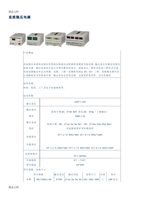
直流稳压电源TX1715SL1A-2AProduct InformationSUMMARIZE:The DC Power supply is automatic constant-voltage/constant-currenttransfer type of power supply with display meter(3-1/2 digits, liquidcrystal display) or electrical point meter. Output constant voltage isadjusted 15V and output constant current is 2A,0-1A/2Ait is output type have one, two and two with fixed 5V3A.The output canbe connected in paralleled or series to get multiple output currents or voltages. APPLICATION:Scientific research, educational institutions factoryand electronics electrical equipment repairs etc.MAIN FUNCTION:1. Output constant current adjustable.2. Output constant voltage adjustable.3. LED display.4. Limited current protection.5. Short circuit protection.CHARACTERISTIC:Input voltage:220VAC±10%Output voltage:0-15/DC;fix 5V3AOutput current:0-1A/2A.Frequency: 50Hz±2HzUsage area: scientific research, educational institutions, factory andelectronics, electrical equipment repairs, ets.DIMENSIONS AND WEIGHT:Model:SK1715SL1A-2AQty:8 PCSPackage: dimension: 585x375x355mmDisplay: 1×LCDG.W.:19.5kgTX1731SBP 1-5AProduct InformationSUMMARIZE:The DC Power supply is automatic constant-voltage/constant-currenttransfer type of power supply with display meter(3-1/2 digits, liquidcrystal display) or electrical point meter. Output constant voltage isadjusted 0-30V and output constant current is 5A,0-1A/2A/3A/5AIt is output type have one, two and two with fixed 5V3A.T he output canbe connected in paralleled or series to get multiple output currents or voltages. APPLICATION:Scientific research, educational institutions factoryand electronics electrical equipment repairs etc.MAIN FUNCTION:1. Output constant current adjustable.2. Output constant voltage adjustable.3. LCD, display.4. Limited current protection.5. Short circuit protection.CHARACTERISTIC:Input voltage:220VAC±10%Output voltage:0-30/60 DC; fix 5V3AOutput current:0-1A/2A/3AFrequency: 50Hz±2HzUsage area: scientific research, educational institutions, factory and electronics, electrical equipment repairs, ets.DIMENSIONS AND WEIGHT:Model:SK1731SBP 1-5AQty: 2 PCSPackage: dimension: 475x345x530mmDisplay: 2×LCDG.W.:26.5/29.5/31kgTX1731SB1A-5AProduct InformationSUMMARIZE:The DC Power supply is automatic constant-voltage/constant-current transfer type of power supply with display meter(3-1/2 digits, liquidcrystal display) or electrical point meter. Output constant voltage isadjusted 0-30V/60V and output constant current is 5A,0-1A/2A/3A/5A It is output type have one, two and two with fixed 5V3A.The output canbe connected in paralleled or series to get multiple output currents or voltages.APPLICATION:Scientific research, educational institutions factoryand electronics electrical equipment repairs etc.MAIN FUNCTION:1. Output constant current adjustable.2. Output constant voltage adjustable.3. LCD display.4. Limited current protection.5. Short circuit protection.CHARACTERISTIC:Input voltage:220VAC±10%Output voltage:0-30/60VDC;fix 5V3AOutput current:0-1A/2A/3A.Frequency: 50Hz±2HzUsage area: scientific research, educational institutions, factory andelectronics, electrical equipment repairs, ets.DIMENSIONS AND WEIGHT:Model:SK1731SL1A-5AQty: 2 PCSPackage: dimension: 455x360x480mmDisplay: 4×LEDG.W.:27/29.5/31.5/31kgTX1760SL1A-3AProduct InformationSUMMARIZE:The DC Power supply is automatic constant-voltage/constant-currenttransfer type of power supply with display meter(3-1/2 digits, liquidcrystal display) or electrical point meter. Output constant voltage isadjusted 0-30V/60V and output constant current is 5A,0-1A/2A/3A/5AIt is output type have one, two and two with fixed 5V3A.The output canbe connected in paralleled or series to get multiple output curren ts or voltages. APPLICATION:Scientific research, educational institutions factoryand electronics electrical equipment repairs etc.MAIN FUNCTION:1. Output constant current adjustable.2. Output constant voltage adjustable.3. LCD, display.4. Limited current protection.5. Short circuit protection.CHARACTERISTIC:Input voltage:220VAC±10%Output voltage:0-30/60VDC;fix 5V3AOutput current:0-1A/2A/3AFrequency: 50Hz±2HzUsage area: scientific research, educational institutions, factory and electronics, electrical equipment repairs, ets.DIMENSIONS AND WEIGHT:Model:SK1760SL1A-3AQty: 4PCSPackage: dimension: 425x385x596mmDisplay: 2×LEDG.W.:22/33/24kg。
开关电源外文翻译()

开关电源外文翻译()————————————————————————————————作者:————————————————————————————————日期:Modeling, Simulation, and Reduction of Conducted Electromagnetic Interference Due to a PWM Buck Type Switching Power Supply IA. FarhadiAbstract:Undesired generation of radiated or conducted energy in electrical systems is called Electromagnetic Interference (EMI). High speed switching frequency in power electronics converters especially in switching power supplies improves efficiency but leads to EMI. Different kind of conducted interference, EMI regulations and conducted EMI measurement are introduced in this paper. Compliancy with national or international regulation is called Electromagnetic Compatibility (EMC). Power electronic systems producers must regard EMC. Modeling and simulation is the first step of EMC evaluation. EMI simulation results due to a PWM Buck type switching power supply are presented in this paper. To improve EMC, some techniques are introduced and their effectiveness proved by simulation.Index Terms:Conducted, EMC, EMI, LISN, Switching SupplyI. INTRODUCTIONFAST semiconductors make it possible to have high speed and high frequency switching in power electronics []1. High speed switching causes weight and volume reduction of equipment, but some unwanted effects such as radio frequency interference appeared []2. Compliance with electromagnetic compatibility (EMC) regulations is necessary for producers to present their products to the markets. It is important to take EMC aspects already in design phase []3. Modeling and simulation is the most effective tool to analyze EMC consideration before developing the products. A lot of the previous studies concerned the low frequency analysis of power electronics components []4[]5. Different types of power electronics converters are capable to be considered as source of EMI. They could propagate the EMI in both radiated and conducted forms. Line Impedance Stabilization Network (LISN) is required for measurement and calculation of conducted interference level []6. Interference spectrum at the output of LISN is introduced as the EMC evaluation criterion []7[]8. National or international regulations are the references for the evaluation of equipment in point of view of EMC []7[]8.II. SOURCE, PATH AND VICTIM OF EMIUndesired voltage or current is called interference and their cause is called interferencesource. In this paper a high-speed switching power supply is the source of interference.Interference propagated by radiation in area around of an interference source or by conduction through common cabling or wiring connections. In this study conducted emission is considered only. Equipment such as computers, receivers, amplifiers, industrial controllers, etc that are exposed to interference corruption are called victims. The common connections of elements, source lines and cabling provide paths for conducted noise or interference. Electromagnetic conducted interference has two components as differential mode and common mode []9.A. Differential mode conducted interferenceThis mode is related to the noise that is imposed between different lines of a test circuit by a noise source. Related current path is shown in Fig. 1 []9. The interference source, path impedances, differential mode current and load impedance are also shown in Fig. 1.B. Common mode conducted interferenceCommon mode noise or interference could appear and impose between the lines, cables or connections and common ground. Any leakage current between load and common ground could be modeled by interference voltage source.and Fig. 2 demonstrates the common mode interference source, common mode currents Icm1 and the related current paths[]9.The power electronics converters perform as noise source Icm2between lines of the supply network. In this study differential mode of conducted interference is particularly important and discussion will be continued considering this mode only.III. ELECTROMAGNETIC COMPATIBILITY REGULATIONS Application of electrical equipment especially static power electronic converters in different equipment is increasing more and more. As mentioned before, power electronics converters are considered as an important source of electromagnetic interference and have corrupting effects on the electric networks []2. High level of pollution resulting from various disturbances reduces the quality of power in electric networks. On the other side some residential, commercial and especially medical consumers are so sensitive to power system disturbances including voltage and frequency variations. The best solution to reduce corruption and improve power quality is complying national or international EMC regulations. CISPR, IEC, FCC and VDE are among the most famous organizations from Europe, USA and Germany who are responsible for determining and publishing the most important EMC regulations. IEC and VDE requirement and limitations on conducted emission are shown in Fig. 3 and Fig. 4 []7[]9.For different groups of consumers different classes of regulations could be complied. Class A for common consumers and class B with more hard limitations for special consumers are separated in Fig. 3 and Fig. 4. Frequency range of limitation is different for IEC and VDE that are 150 kHz up to 30 MHz and 10 kHz up to 30 MHz respectively. Compliance of regulations isevaluated by comparison of measured or calculated conducted interference level in the mentioned frequency range with the stated requirements in regulations. In united European community compliance of regulation is mandatory and products must have certified label to show covering of requirements []8.IV. ELECTROMAGNETIC CONDUCTED INTERFERENCE MEASUREMENTA. Line Impedance Stabilization Network (LISN)1-Providing a low impedance path to transfer power from source to power electronics converter and load.2-Providing a low impedance path from interference source, here power electronics converter, to measurement port.Variation of LISN impedance versus frequency with the mentioned topology is presented inFig. 7. LISN has stabilized impedance in the range of conducted EMI measurement []7.Variation of level of signal at the output of LISN versus frequency is the spectrum of interference. The electromagnetic compatibility of a system can be evaluated by comparison of its interference spectrum with the standard limitations. The level of signal at the output of LISN in frequency range 10 kHz up to 30 MHz or 150 kHz up to 30 MHz is criterion of compatibility and should be under the standard limitations. In practical situations, the LISN output is connected to a spectrum analyzer and interference measurement is carried out. But for modeling and simulation purposes, the LISN output spectrum is calculated using appropriate software.For a simple fixed frequency PWM controller that is applied to a Buck DC/DC converter, it is) changes slow with respect to the switching frequency, the possible to assume the error voltage (vepulse width and hence the duty cycle can be approximated by (1). Vp is the saw tooth waveform amplitude.A. PWM waveform spectral analysisThe normalized pulse train m (t) of Fig. 8 represents PWM switch current waveform. The nth pulse of PWM waveform consists of a fixed component D/fs , in which D is the steady state duty cycle, and a variable component dn/f sthat represents the variation of duty cycle due to variation of source, reference and load.As the PWM switch current waveform contains information concerning EMI due to powersupply, it is required to do the spectrum analysis of this waveform in the frequency range of EMI studies. It is assumed that error voltage varies around V e with amplitude of V e1 as is shown in (2).fm represents the frequency of error voltage variation due to the variations of source, reference and load. The interception of the error voltage variation curve and the saw tooth waveform with switching frequency, leads to (3) for the computation of duty cycle coefficients []10.Maximum variation of pulse width around its steady state value of D is limited to D1. In each period of Tm=1/fm , there will be r=fs/fm pulses with duty cycles of dn. Equation (4) presents the Fourier series coefficients Cn of the PWM waveform m (t). Which have the frequency spectrum of Fig.9.B-Equivalent noise circuit and EMI spectral analysisTo attain the equivalent circuit of Fig.6 the voltage source Vs is replaced by short circuit and) as it has shown in Fig. 10. converter is replaced by PWM waveform switch current (IexThe transfer function is defined as the ratio of the LISN output voltage to the EMI current source as in (5).The coefficients di, ni (i = 1, 2, … , 4) correspond to the parameters of the equivalent circuit. Rc and Lc are respectively the effective series resistance (ESR) and inductance (ESL) of the filter capacitor Cf that model the non-ideality of this element. The LISN and filter parameters are as follows: CN = 100 nF, r = 5 Ω, l = 50 uH, RN =50 Ω, LN=250 uH, Lf = 0, Cf =0, Rc= 0, Lc= 0, fs =25 kHzThe EMI spectrum is derived by multiplication of the transfer function and the source noise spectrum. Simulation results are shown in Fig. 11.VI. PARAMETERS AFFECTION ON EMIA. Duty CycleThe pulse width in PWM waveform varies around a steady state D=0.5. The output noise spectrum was simulated with values of D=0.25 and 0.75 that are shown in Fig. 12 and Fig. 13. Even harmonics are increased and odd ones are decreased that is desired in point of view of EMC.On the other hand the noise energy is distributed over a wider range of frequency and the level of EMI decreased []11.B. Amplitude of duty cycle variationThe maximum pulse width variation is determined by D1. The EMI spectrum was simulatedwith D1=0.05. Simulations are repeated with D1=0.01 and 0.25 and the results are shown in Fig.14and Fig.15.Increasing of D1 leads to frequency modulation of the EMI signal and reduction in level of conducted EMI. Zooming of Fig. 15 around 7th component of switching frequency in Fig. 16 shows the frequency modulation clearly.C. Error voltage frequencyThe main factor in the variation of duty cycle is the variation of source voltage. The fm=100 Hz ripple in source voltage is the inevitable consequence of the usage of rectifiers. The simulation is repeated in the frequency of fm=5000 Hz. It is shown in Fig. 17 that at a higher frequency for fm the noise spectrum expands in frequency domain and causes smaller level of conducted EMI. On the other hand it is desired to inject a high frequency signal to the reference voltage intentionally.D. Simultaneous effect of parametersSimulation results of simultaneous application of D=0.75, D1=0.25 and fm=5000 Hz that leadto expansion of EMI spectrum over a wider frequencies and considerable reduction in EMI level is shown in Fig. 18.VII. CONCLUSIONAppearance of Electromagnetic Interference due to the fast switching semiconductor devices performance in power electronics converters is introduced in this paper. Radiated and conducted interference are two types of Electromagnetic Interference where conducted type is studied in this paper. Compatibility regulations and conducted interference measurement were explained. LISN as an important part of measuring process besides its topology, parameters and impedance were described. EMI spectrum due to a PWM Buck type DC/DC converter was considered and simulated. It is necessary to present mechanisms to reduce the level of Electromagnetic interference. It shown that EMI due to a PWM Buck type switching power supply could be reduced by controlling parameters such as duty cycle, duty cycle variation and reference voltage frequency.VIII. REFRENCES[1] Mohan, Undeland, and Robbins, “Power Electronics Converters, Applications and Design” 3rdedition, John Wiley & Sons, 2003.[2] P. Moy, “EMC Related Issues for Power Electronics”, IEEE, Automotive Pow er Electronics, 1989, 28-29 Aug. 1989 pp. 46 – 53.[3] M. J. Nave, “Prediction of Conducted Interference in Switched Mode Power Supplies”, Session 3B, IEEE International Symp. on EMC, 1986.[4] Henderson, R. D. and Rose, P. J., “Harmonics and their Effec ts on Power Quality and Transformers”, IEEE Trans. On Ind. App., 1994, pp. 528-532.[5] I. Kasikci, “A New Method for Power Factor Correction and Harmonic Elimination in Power System”, Proceedings of IEEE Ninth International Conference on Harmonics and Q uality of Power, Volume 3, pp. 810 – 815, Oct. 2000.[6] M. J. Nave, “Line Impedance Stabilization Networks: Theory and Applications”, RFI/EMI Corner, April 1985, pp. 54-56.[7] T. Williams, “EMC for Product Designers” 3rd edition 2001 Newnes.[8] B. Ke isier, “Principles of Electromagnetic Compatibility”, 3rd edition ARTECH HOUSE 1987.[9] J. C. Fluke, “Controlling Conducted Emission by Design”, Vanhostrand Reinhold 1991.[10] M. Daniel,”DC/DC Switching Regulator Analysis”, McGrawhill 1988[11] M. J. Nave,” The Effect of Duty Cycle on SMPS Common Mode Emission: theory and experiment”, IEEE National Symposium on Electromagnetic Compatibility, Page(s): 211-216, 23-25 May 1989.作者:A. Farhadi国籍:伊朗出处:基于压降型PWM开关电源的建模、仿真和减少传导性电磁干扰IIA. Farhadi作者:A. Farhadi国籍:伊朗出处:摘要:电子设备之中杂乱的辐射或者能量叫做电磁干扰(EMI)。
- 1、下载文档前请自行甄别文档内容的完整性,平台不提供额外的编辑、内容补充、找答案等附加服务。
- 2、"仅部分预览"的文档,不可在线预览部分如存在完整性等问题,可反馈申请退款(可完整预览的文档不适用该条件!)。
- 3、如文档侵犯您的权益,请联系客服反馈,我们会尽快为您处理(人工客服工作时间:9:00-18:30)。
单位代码01学号分类号密级文献翻译高精度稳压直流电源院(系)名称信息工程学院专业名称电子信息工程学生姓名指导教师2013年3 月30 日高精度稳压直流电源文摘:目前对于可调式直流电源的设计和应用现在有很多微妙的,多种多样的,有趣的问题。
探讨这些问题(特别是和中发电机组有关),重点是在电路的经济适用性上,而不是要达到最好的性能。
当然,对那些精密程度要求很高的除外。
讨论的问题包括温度系数,短期漂移,热漂移,瞬态响应变性遥感和开关preregualtor型机组及和它的性能特点有关的一些科目。
介绍从商业的角度来看供电领域可以得到这样一个事实,在相对较低的成本下就可以获得标准类型的0.01%供电调节。
大部分的供电用户并不需要这么高的规格,但是供应商不会为了减少客户这么一点的费用而把0.1%改成0.01%。
并且电力供应的性能还包括其他一些因素,比如说线路和负载调解率。
本文将讨论关于温度系数、短期漂移、热漂移,和瞬态的一些内容。
目前中等功率直流电源通常采用预稳压来提高功率/体积比和成本,但是只有某些电力供应采用这样的做法。
这种技术的优缺点还有待观察。
温度系数十年以前,大多数的商业电力供应为规定的0.25%到1%。
这里将气体二极管的温度系数定位百分之0.01。
因此,人们往往会忽视TC(温度系数)是比规定的要小的。
现在参考的TC往往比规定的要大的多。
为了费用的减少,后者会有很大的提高,但是这并不是真正的TC。
因此,如果成本要保持在一个低的水平,可以采用TC非常低的齐纳二极管,安装上差动放大电路,还要仔细的分析低TC绕线电阻器。
如图1所示,一个典型的放大器的第一阶段,其中CR1是参考齐纳二极管,R是输出电位调节器。
图1 电源输入级图2 等效的齐纳参考电路假设该阶段的输出是e3,提供额外的差分放大器,在稳定状态下e3为零,任何参数的变化都会引起输出的漂移;对于其他阶段来说也是一样的,其影响是减少了以前所有阶段的增益。
因此,其他阶段的影响将被忽略。
以下讨论的内容涵盖了对于TC整体的无论是主要的还是次要的影响。
R3的影响CR1-R3分支的等效的电路如图2所示,将齐纳替换成了它的等效电压源E'和内部阻抗R2。
对于高增益调节器,其中R3的变化对差分放大器的输入来说可以忽略不计,所以前后的变化由R3决定。
如果进一步假定IB << Iz;从(1)可以得到同时,消除Iz,由(2b)可得并且现在,假设那么,方程式(2b)也可以写成例1:短期漂移短期漂移是由国家电气制造商协会(NEMA)提供,可以这样说“这段时间的输出与输入,环境和负载无关”。
在上一节中对温度系数的描述在这里也适用。
据试验测定,在电源里面和它附近的热空气极大地提高了短期特性。
流动空气的冷却效果是众所周知的,然而人们通常不会意识到就算空气在齐纳二极管和晶体管中移动的很缓慢,它对温度的影响也是很显著地。
如果提供比较大的TC,那么输出会有很大的变化。
会有低TC 实现补偿,也就是说,如果消除了了一些元器件相同或相反的影响,这些元器件的热时间常数仍会受到干扰。
一个常用的方法是使用第一个放大器来消除和平衡掉交界处冷却效果上的差异。
可以通过晶体管的固定或保持来近似模拟这个方案,将晶体管嵌入在一个共同的金属块中,等等。
笔者通过把输入级和参考齐纳放置到一个单独的机箱中取得了很好的效果。
如图4所示。
在图5中通过金属的覆盖,漂移得到了很好的改善。
图3 12V的电源晶体管具有百分之0.01的调节精度。
注:保护盒是用来给第一放大器和参考组件进行隔热保护。
图4电源晶体管的测试图图4和图3类似,电源提供了短期漂移,并且没有保护措施。
该元件是没有覆盖直到t1。
盒子里面的温度上升,电压随着时间t1而变化。
如果电位器用于输出地调节(例如R1),应该谨慎的选择价位和设计。
接触电阻的变化可引起漂移。
用有高精密线圈的元件来获得低漂移是没有必要的。
用低电阻的合金和低分辨率的元件可以轮流休息,来缩小范围可以达到同样令人满意的效果。
当然,还要考虑到线路的抗腐蚀性等问题。
有机硅润滑脂可以得到很好的效果。
接触臂的周期的运用对元件的腐蚀有很好的“疗效”。
热漂移符合NEMA定义的热漂移就是“由于不正常的环境的变化引起有关的内部环境温度的变化而照成在一定时间内输出的变化。
温漂通常与线路电压和负载有关”。
温漂与TC的供应以及整体散热的设计有关。
通过对关键部件妥善安置是有可能大大减少甚至完全消除影响。
百分之0.01(规定)的耗材有满负载的百分之0.05到0.15之间的漂移,这非常的罕见。
事实上,一个制造商曾经说过百分之0.15会更好。
减少热漂移除了提高TC以外还可以通过减少内部的消耗来解决。
比如说在关键的放大器和散热元件之间放置热障。
外表面最好位于通风良好处。
应该注意到,只能在百分之0.01和0.05之间索取。
瞬态响应大多数该类型的电源有一个还很受争议的负载端电容器。
这是出于稳定的目的,通常会决定主要的电源时间常数。
这个电容器会导致在遥感模式下短暂的电力供应不良的现象①。
通常情况下,晶体管电源会在很短的时间内作出反应,但是笔者曾经指出,在遥感时,反应会变得很小。
其等效电源如图5所示。
引线从电源到负载电阻R处引入,设备的感应电流Is是相对稳定的。
在平衡条件下,图6表明,一个突然的负荷变化会导致Ldi/dt的瞬间激增,我们称之为“尖峰”;以及线性放电时间越长时电容充放电的情况。
放电时间是,其中并且,①对于Is来说,通常它不会在放大器的最后阶段提供驱动,但是会出现限流现象。
遥感是指电源电压电感的直接负荷。
图5 远程输出传感的等效电路图6 瞬态响应,遥感。
图7 框图。
使用预稳压电源可以减少监测和控制的A型阶段电压的使用和损耗。
由于主要的调节器往往比预调节器响应更快,应该建立足够的储备来使这个阶段下降。
如果不这样可能会导致负载的饱和,那是前置稳压器在响应时间内产生的。
开关前置稳压器型机组传统类- A型晶体管电源供应变得相当笨重,昂贵,与传递阶段拥挤,作为供给增加电流和功率的水平。
要求输出调节范围更大,再加上电力的供应是远程可编程的,会极大地提高条件的要求。
正是由于这些原因,高效利用的开关调节器作为一种压力调节阀在商业和军事用品应用了许多年。
绝大多数的供应整流器可控硅使用与控制元件。
从60-cycle操作的系统压力调节阀响应来源,在20至50ms之间。
最近对高压、大功率开关晶体管的方法更具有吸引力。
该系统提供了一种低成本,发行量较小的方法,再加上一个submillisecond响应时间。
通常是独立的电源频率导致了高开关率。
开关频率就可能被固定的,一个被控制的变量或一个独立的自生自储(LC滤波器电路)参数。
更快的反应时间是非常可取的,因为它减少了在预备役电压值必须通过阶段或仓库(的数量)的电力需求在压力调节阀过滤器。
一个晶体管作为电源开关操作适合具有大电流,高电压等级低漏电流耦合。
不幸的是,这些特点是实现了热容量牺牲,同时使电压和电流的条件导致很高的峰值功率可能是灾难性的。
因此,它成为强制性的设计负荷高峰期间有足够的条件,也包含开关驱动电流限制或快速过载保护系统。
商业发展电力供应总是有输出电流限制,但这并不限制压力调节阀电流负载条件下,除了在稳态(包括短路)。
考虑一下,例如,一个电源工作在短路、短被删除突然叫起来。
指图8、9月的产量将会快速上涨,减少通过阶段电压,关闭开关晶体管。
由此产生的瞬态传达很多周期的交换率),这样电感的压力调节阀过滤变得完全不够的限制流量。
因此,当前将会上升直至稳态已恢复、电路电阻引起限制,或不足开车使开关出来的饱和度。
上述第二种情况导致开关失败。
其他营业状况会产生相似的瞬变包括输出电压编程和初始刺激的用度。
输入功率瞬间的中断也应首先要考虑的事。
一个解决这个问题的办法就是限制的电压变化的速率在可出现一值,通过舞台了压力调节阀可以遵循。
这能被做方便加上足够的输出电容。
这电容会同限流特性会产生一种最大的改变的比率其中C0 = output capacity.假设这个压力调节阀遵循这种变化和有滤波电容器,然后开关电流在电源在上,压力调节阀的参考电压上升也必须是有限的。
采取这一考虑,其中ER = passing stage voltageTl = time constant of reference supply.策略合作关系SCR的使用来代替电晶体的将是一个明显改善由于较高的增兵电流的收视率,却转身他们去了,需要大量的能源。
而门策略合作关系SCR讨厌似乎将为员工提供良好的折衷,全部的问题,严峻的限制,在当前的收视率现限制使用它们。
本文摘自:IEEE TRANSACTIONS ON INDUSTRY AND GENERAL APPLICATIONS VOL. IGA-2, NO.5 SEPT/OCT 1966附:英文原文Highly Regulated DC Power SuppliesAbstract-The design and application of highly regulated dc power supplies present many subtle, diverse, and interesting problems. This paper discusses some of these problems (especially inconnection with medium power units) but emphasis has been placed more on circuit economics rather than on ultimate performance.Sophisticated methods and problems encountered in connection with precision reference supplies are therefore excluded. The problems discussed include the subjects of temperature coefficient,short-term drift, thermal drift, transient response degeneration caused by remote sensing, and switchingpreregualtor-type units and some of their performance characteristics. INTRODUCTIONANY SURVEY of the commercial de power supply field will uncover the fact that 0.01 percent regulated power supplies are standard types and can be obtained at relatively low costs. While most users of these power supplies do not require such high regulation, they never-theless get this at little extra cost for the simple reason that it costs the manufacturer very little to give him 0.01 percent instead of 0.1 percent. The performance of a power supply, however, includes other factors besides line and load regulation. This paper will discuss a few of these-namely, temperature coefficient, short-term drift, thermal drift, and transient response. Present medium power dc supplies commonly employ preregulation as a means of improving power/volume ratios and costs, but some characteristics of the power supply suffer by this approach. Some of the short-comings as well as advantages of this technology will be examined.TEMPERATURE COEFFICIENTA decade ago, most commercial power supplies were made to regulation specifications of0.25 to 1 percent. The reference elements were gas diodes having temperature coefficients of the order of 0.01 percent. Consequently, the TC (temperature coefficient) of the supply was small compared to the regulation specifications and often ignored. Today, the reference element often carries aTC specification greater than the regulation specification.While the latter may be improved considerably at little cost increase, this is not necessarily true of TC. Therefore,the use of very low TC zener diodes, matched differential amplifier stages, and low TC wire wound resistors must be analyzed carefully, if costs are to be kept low.A typical first amplifier stage is shown in Fig. 1. CRI is the reference zener diode and R, is the output adjustment potentiometer.Fig. 1. Input stage of power supply.Fig. 2. Equivalent circuit of zener reference.Let it be assumed that e3, the output of the stage, feedsadditional differential amplifiers,and under steady-state conditions e3 = 0. A variation of any of the parameters could cause the output to drift; while this is also true of the other stages, the effects are reduced by the gain of all previous stages. Consequently, the effects of other stages will be neglected. The following disculssion covers the effects of all elements having primary and secondary influences on the overall TC.Effect of R3The equivalent circuit of CRI -R3 branch is shown in Fig. 2. The zener ha's been replaced with its equivalent voltage source E/' and internal impedance R,. For high gain regulators, the input of the differential amplifier will have negligible change with variations of R3 so thatbefore and after a variation of R3 is made.If it is further assumed that IB << Iz; then from (1)Also,Eliminating I, from (2b),andNow, assuming thatthen,Equation (2b) can also be writtenSHORT-TERM DRIFTThe short-term drift of a supply is defined by the National Electrical Manufacturers Association (NEMA) as "a change in output over a period of time, which change is unrelated to input, environment, or load."Much of the material described in the section on temperature coefficient is applicable here as well. It has been determined experimentally, however, that thermal air drafts in and near the vicinity of the power supply contributes enormously to the short-term characteristics. The cooling effects of moving air are quite well known, but it is not often recognized that even extremely slow air movements over such devices as zeners and transistors cause the junction temperature of these devices to change rapidly. If the TC of the supply is large compared to the regulation, then large variations in the output will be observed. Units having low TC's achieved by compensation-that is, by canceling out the effects of some omponents by equal and opposite effects of others may still be plagued by these drafts due tothe difference in thermal time constants of the elements.Oftentimes, a matched transistor differential amplifier in a common envelope is used for the first amplifier just to equalize and eliminate the difference in cooling effects between the junctions. Approximations to this method include cementing or holding the transistors together, imbedding the transistors in a common metal block, etc. Excellent results were achieved by the author by placing the input stage and zener reference in a separate enclosure. This construction is shown in Fig. 4. The improvement in drift obtained by means of the addition of the metal cover is demonstrated dramatically in Fig. 5.Fig. 5. Short-term drift of a power supply similar to the one shown in Fig. 4 with and without protective covers. The unit was operated without the cover until time tl, when the cover was attached. The initial voltage change following t, is due to a temperature rise inside the box.Fig. 5. Short-term drift of a power supply similar to the one shown n Fig. 4 with and without protective covers. The unit was operated without the cover until time tl, when the cover was attached. The initial voltage change following t, is due to a temperature rise inside the box.If potentiometers are used in the supply for output adjustment (e.g., RI), care should be used in choosing the value and design. Variations of the contact resistance can cause drift. It is not always necessary, however, to resort to the expense of high-resolution multiturn precision units to obtain low drift. A reduction in range of adjustment, use of low-resistance alloys and low-resolution units which permit the contact arm to rest firmly between turns, may be just as satisfactory. Of course, other considerations should include the ability of both the arms and the wire to resist corrosion. Silicone greases are helpful here. Periodic movement of contact arms has been found helpful in "healing" corroded elements.THERMAL DRIFTNEMA defines thermal drift as "a change in output over a period of time, due to changes in internal ambient temperatures not normally related to environmental changes. Thermal drift is usually associated with changes in line voltage and/or load changes ."Thermal drift, therefore, is strongly related to the TC of the supply as well as its overall thermal design. By proper placement of critical components it is possible to greatly reduce or even eliminate the effect entirely. It is not uncommon for supplies of the 0.01 percent(regulation) variety to have drifts of between 0.05 to 0.15 percent for full line or full load variations. In fact, one manufacturer has suggested that anything better than 0.15 percent is good. Solutions to reducing thermal drift other than the obvious approach of improving the TC and reducing internal losses include a mechanical design that sets up a physical and thermal barrier between the critical amplifier components and heat dissipating elements. Exposure to outside surfaces with good ventilation is recommended. With care, 0.01 to 0.05 percent is obtainable.TRANSIENT RESPONSEMost power supplies of the type being discussed have a capacitor across the load terminals. This is used for stabilization purposes and usually determines the dominant time constant of the supply. The presence of this capacitor unfortunately leads to undesirable transient phenomena when the supply is used in the remote sensing mode①. Normally, transistorized power supplies respond in microseconds, but as the author has pointed out , the response can degenerate severely in remote sensing .The equivalent circuit is shown in Fig. 5. The leads from the power supply to the load introduce resistance r. Is is the sensing current of the supply and is relatively constant.Under equilibrium conditions,A sudden load change will produce the transient of Fig. 6. The initial "spike" is caused by an inductive surge Ldi/dt; the longer linear discharge following is the result of the capacitor trying to discharge (or charge). The discharge time iswhereandThe limitations of I,, are usually not due to available drive of the final amplifier stages but to other limitations, current limiting being the most common. Units using pre regulators of the switching type (transistor or SCR types) should be looked at carefully if the characteristics mentioned represent a problem.①Remote sensing is the process by which the power supply senses voltage directly at the load.Fig. 5. Output equivalent circuit at remote sensing.Fig. 6. Transient response, remote sensing.Fig. 7. Block diagram.Preregulated supplies are used to reduce size and losses by monitoring and controlling the voltage across the class-A-type series passing stage (Fig. 7). Since the main regulator invariably responds much quicker than the preregulator, sufficient reserve should always be built into the drop across the passing stage. Failure to provide this may result in saturation of the passing stage when load is applied, resulting in a response time which is that of the preregulator itself.SWITCHING PREREGULATOR-TYPE UNITSThe conventional class-A-type transistorized power supply becomes rather bulky, expensive, and crowded with passing stages, as the current and power level of the supply increases. The requirement of wide output adjustment range, coupled with the ability of thesupply to be remotely programmable, aggravates the condition enormously. For these reasons the high-efficiency switching regulator has been employed as a preregulator in commercial as well as military supplies for many years. The overwhelming majority of the supplies used silicon controlled rectifiers as the control element. For systems operating from 60-cycle sources, this preregulator responds in 20 to 50 ms.Recent improvements in high-voltage, high-power switching transistors has made the switching transistor pproach more attractive. This system offers a somewhat lower-cost, lower-volume approach coupled with a submillisecond response time. This is brought about by a high switching rate that is normally independent of line frequency. The switching frequency may be fixed, a controlled variable or an independent self-generated (by the LC filter circuit) parameter. Faster response time is highly desirable since it reduces the amount of reserve voltage required across the passing stage or the amount of (storage) capacity required in the preregulator filter.A transistor suitable for operating as a power switch has a high-current, high-voltage rating coupled with low leakage current. Unfortunately, these characteristics are achieved by a sacrifice in thermal capacity, so that simultaneous conditions of voltage and current leading to high peak power could be disastrous. It therefore becomes mandatory to design for sufficient switch drive during peak load conditions and also incorporate current-limiting or rapid overload protection systems.Commercial wide-range power supplies invariably have output current limiting, but this does not limit the preregulator currents except during steady-state load conditions (including short circuits). Consider, for example, a power supply operating at short circuit and the short being removed suddenly. Referring to Fig. 7, the output would rise rapidly, reduce the passing stage voltage, and close the switching transistor. The resulting transient extends over many cycles (switching rate) so that the inductance of the preregulator filter becomes totally inadequate to limit current flow. Therefore, the current will rise until steady state is resumed, circuit resistance causes limiting, or insufficient drive causes the switch to come out ofsaturation. The latter condition leads to switch failure.Other operating conditions that would produce similar transients include output voltage programming and initial turn-on of the supply. Momentary interruption of input power should also be a prime consideration.One solution to the problem is to limit the rate of change of voltage that can appear across the passing stage to a value that the preregulator can follow. This can be done conveniently by the addition of sufficient output capacitance. This capacitance in conjunction with the current limiting characteristic would produce a maximum rate of change ofwhereC0 = output capacity.Assuming that the preregulator follows this change and has a filter capacitor Cl, then the switch current isDuring power on, the preregulator reference voltage rise must also be limited. Taking this into account,whereER = passing stage voltageTl = time constant of reference supply.The use of SCR's to replace the transistors would be a marked improvement due to黄河科技学院毕业设计(文献翻译)第20页higher surge current ratings, but turning them off requires large energy sources. While the gate turn-off SCR seems to offer a good compromise to the overall problem, the severe limitations in current ratings presently restrict their use.from:IEEE TRANSACTIONS ON INDUSTRY AND GENERAL APPLICATIONS VOL. IGA-2, NO.5 SEPT/OCT 1966。