DDR3_desigin guide_V1.3
DDR3硬件电路设计——经验

DDR3硬件电路设计——经验随着CPU 性能不断提高,我们对内存性能的要求也逐步升级。
不可否认,紧紧依高频率提升带宽的DDR迟早会力不从心,因此JEDEC 组织很早就开始酝酿DDR2 标准,加上LGA775接口的915/925以及最新的945等新平台开始对DDR2内存的支持,所以DDR2内存将开始演义内存领域的今天。
DDR2 能够在100MHz 的发信频率基础上提供每插脚最少400MB/s 的带宽,而且其接口将运行于1.8V 电压上,从而进一步降低发热量,以便提高频率。
此外,DDR2 将融入CAS、OCD、ODT 等新性能指标和中断指令,提升内存带宽的利用率。
从JEDEC组织者阐述的DDR2标准来看,针对PC等市场的DDR2内存将拥有400、533、667MHz等不同的时钟频率。
高端的DDR2内存将拥有800、1000MHz两种频率。
DDR-II内存将采用200-、220-、240-针脚的FBGA封装形式。
最初的DDR2内存将采用0.13微米的生产工艺,内存颗粒的电压为1.8V,容量密度为512MB。
内存技术在2005年将会毫无悬念,SDRAM为代表的静态内存在五年内不会普及。
QBM与RDRAM内存也难以挽回颓势,因此DDR 与DDR2共存时代将是铁定的事实。
PC-100的“接班人”除了PC一133以外,VCM(VirXual Channel Memory)也是很重要的一员。
VCM即“虚拟通道存储器”,这也是目前大多数较新的芯片组支持的一种内存标准,VCM内存主要根据由NEC公司开发的一种“缓存式DRAM”技术制造而成,它集成了“通道缓存”,由高速寄存器进行配置和控制。
在实现高速数据传输的同时,VCM还维持着对传统SDRAM的高度兼容性,所以通常也把VCM内存称为VCM SDRAM。
VCM与SDRAM 的差别在于不论是否经过CPU处理的数据,都可先交于VCM进行处理,而普通的SDRAM 就只能处理经CPU处理以后的数据,所以VCM要比SDRAM 处理数据的速度快20%以上。
DDR3 硬件设计和 Layout 设计【中为电子科技工作室.】

DDR3硬件设计和Layout设计译自飞思卡尔官方文档Hardware and Layout Design Considerations for DDR3 SDRAMMemory Interfaces目录1 设计检查表 (3)2 终端匹配电阻功耗计算 (8)3 VREF (8)4 VTT电压轨 (8)5 DDR布线 (9)5.1 数据线— MDQ[0:63], MDQS[0:8], MDM[0:8], MECC[0:7] (9)5.2 Layout建议 (10)6 仿真 (12)7 扩展阅读 (13)8 历史版本 (13)9 声明 (13)这是一篇关于DDR3 SDRAM IP core的设计向导,出自飞思卡尔,为了实现PCB的灵活设计,我们可以采用合适的拓扑结构简化设计时的板级关联性。
飞思卡尔强烈推荐系统/板级工程师在PCB制板前进行设计验证,包括信号完整性、时序等等。
1 设计检查表如表1,罗列了DDR设计检查清单,推荐逐一检查,并在最右侧作出决策。
MDQSx/x。
DDR3数据线在做蛇形走线等长匹配时,应该保证蛇形走线间至少有25mil 的间距。
2 终端匹配电阻功耗计算DDR的地址线和控制线会有灌电流和拉电流经终端电阻R T流过,那么该电阻的功耗计算如下:Power = x R T = x (47Ω) = 7.5mW根据上述,我们需要选择高达1/16W的电阻。
另外,V TT电流的计算请参看第4节。
3 V REFV REF电流需求相对较小,低于3mA。
V REF是为控制器和DDR芯片的差分接收器提供0.75V 的直流偏置(V DD/2),V REF的误差或噪声可能会在总线上引起时序错误、不期望的抖动和误动作等。
为避免上述问题,V REF噪声必须控制在JEDEC要求范围内,因此,V REF和V TT不能在同一平面,因为DRAM的V REF对V TT的噪声很敏感。
但是,VREF和VTT的产生必须经由同一个电源产生,以保证高度统一,所以每一个VREF要放置合适的去耦电容(包括控制器、每一个DIMM/DDR芯片、V REF电源),并且做到布局布线简单,预防潜在问题。
xilinx平台DDR3设计教程之设计篇_中文版教程3
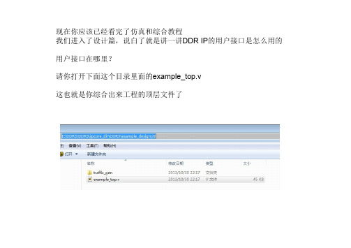
现在你应该已经看完了仿真和综合教程我们进入了设计篇,说白了就是讲一讲DDR IP的用户接口是怎么用的用户接口在哪里?请你打开下面这个目录里面的example_top.v这也就是你综合出来工程的顶层文件了我们来理一理这个文件的结构吧开头部分,全是介绍,你删了都关系然后是各种参数的设定这里有bank,row,column,rank,等等各种设置其实你不用动它们这些都是你之前选条子的时候已经选好了的不记得自己选什么条子了?乖乖,你不如再翻翻仿真教程先?各种仿真延迟参数也跟你选的条子有关你也别管了我都不管这些和DDR条子的各种接口你要知道,用户接口是个内部接口,你这里当然看不到了。
如果之前选了“use system clock”的话这里就看不到clk_ref相关的参考时钟管脚了。
这里顺便提一下column和row地址是在ddr3_addr里面复用的。
column一般是10bit宽度。
row一般14-16bit宽度。
ddr3_ba是选bank的,一般是3bit宽度,对应8个bank。
ddr3_cs_n是选rank的,有几个rank就有几个bit的宽度,因为要考虑啥都不选的情况,和之前几个参数不一样的。
各种参数配置相互之间的关系换算,选择继续和你没有关系作为设计者的你,可以继续无视这些部分各种wire定义你有兴趣研究不?我是没兴趣终于开始实例化DDR3了看见DDR3 右边的#号了没?这说明下面这些都不是管脚,而是配置用的参数。
你继续不用改这都六百多行了,你还是啥也不用改。
唉呀妈呀,DDR3实例化的实体总算找到了,就叫做u_DDR3找到没,我这里是747行接下来你要改动的,其实只有区区几行那就是769行Application interface开始的几个ports从770行的app_addr开始到775行的app_wdf_wren结束一共六行此外,因为你之前选了data mask,所以790行有个app_wdf_mask这一行的赋值你可以直接改成零。
Design Guide for Two DDR3-1066 UDIMM Systems
Technical NoteDesign Guide for Two DDR3-1066 UDIMM SystemsIntroductionDDR3 memory systems are very similar to DDR2 memory systems. One noteworthydifference is the fly-by architecture used in DDR3 JEDEC-standard modules. Dependingon the intended market for the finished product, the memory buses will vary, and thememory system support requirements will range from point-to-point topologies tolarge, multiple registered DIMM topologies.This design guide is intended to assist board designers in developing and implementingtheir products. The document focuses on memory topologies requiring two unbufferedDIMM devices operating at a data rate of 1066Mb/s and two variations of the addressand command bus. The first design variation discussed is a system with one DIMM percopy of the address and command bus using 1T clocking. The second design variation isa system with two DIMM devices on the address and command bus using 2T clocking.The first section of this technical note outlines a set of board design rules, providing astarting point for a board design. The second section details the calculation process fordetermining the portion of the total timing budget allotted to the board interconnect.The intent is that board designers will use the first section to develop a set of generalrules and then, through simulation, verify their designs in the intended environment.Fly-By ArchitectureDesigners who build systems using unbuffered DIMM devices can implement theaddress and command bus using various configurations. For example, some controllershave two copies of the address and command bus, so the system can have one or twoDIMM devices per copy, but no more than two DIMM devices per channel. Further, theaddress bus can be clocked using 1T or 2T clocking. With 1T clocking, a new commandcan be issued on every clock cycle; 2T timing will hold the address and command busvalid for two clock cycles. This reduces the efficiency of the bus to one command per twoclocks, but it substantially increases the amount of setup and hold time available for theaddress and command bus. The data bus remains the same for the address bus varia-tions.DDR3 modules use faster clock speeds than earlier DDR technologies, making signalquality extremely important. For improved signal quality, the clock, control, command,and address buses have been routed in a fly-by topology, where each clock, control,command, and address pin on each DRAM is connected to a single trace and termi-nated. (Other topologies use a tree structure, where termination is off the module nearthe connector.) Inherent to fly-by topology, the timing skew between the clock and DQSsignals can easily be accounted for using the write-leveling feature of DDR3.PDF: 09005aef83a0af6b/Source: 09005aef83657fb2 Micron Technology, Inc., reserves the right to change products or specifications without notice. tn4108_ddr3_design_guide.fm-Rev. B 1/11 EN©2009 Micron Technology, Inc. All rights reserved.The address, command, and control signals are routed on the module with fly-by archi-tecture. As illustrated throughout this technical note, the input signal lines are termi-nated on the module, and further termination is not required. For example, as shown inFigure1 and Figure2 on page3, the V TT terminating resistors are at the end of the fly-bychannel.Figure 1: DDR3-1066 Two-UDIMM Topology – 1T Address and Command BusFigure 2: DDR3-1066 Two-UDIMM Topology – 2T Address and Command BusNote that a timing skew exists between the DRAM controller and the various DRAMdevices on the DIMM, and the DRAM controller must account for the timing skews.DDR3 modules support write leveling, which is intended to help determine the timingskews. For an in-depth discussion of write-leveling features, refer to Micron’s DDR3 datasheets that discuss write leveling.DDR3 Signal GroupsThe signals that compose a DDR3 memory bus can be divided into four unique groups,each with its own configuration and routing requirements.•Data group: Data strobe DQS[8:0], data strobe complement DQS#[8:0], data maskDM[8:0], data DQ[63:0], and check bits CB[7:0] (x72)•Address and command group: Bank addresses BA[2:0]; addresses A[15:0]; andcommand inputs, including RAS#, CAS#, and WE#•Control group:Chip select S#[3:0], clock enable CKE[3:0], on-die terminationODT[3:0], and RESET#0•Clock group: Differential clocks CK[3:0] and CK#[3:0]Board StackupA two-DIMM DDR3 channel can be routed on a four-layer board. The layout should usecontrolled impedance traces of Z O = 40Ω (±10%) characteristic impedance. An exampleboard stackup is shown in Figure3 on page4. The trace impedance is based on a 5-mil-wide trace and 0.5oz copper (Cu) with a dielectric constant of 4.2 for the FR4 prepregmaterial. For this stackup, it is assumed that the 0.5oz Cu on the outer layers is plated fora total thickness of 2.1 mils. Other solutions exist to achieve a 40Ω characteristic imped-ance, so board designers should work with their PCB vendors to specify a stackup.TN-41-08: Design Guide for Two DDR3-1066 UDIMM SystemsDDR3 Command and Address Voltage Margin and Slew Rate Figure 3: Sample Board StackupDDR3 Command and Address Voltage Margin and Slew RateThe primary difference between DDR2 and DDR3 module command, address, andcontrol signals is fly-by topology with impedance matching. Impedance matching isrequired for proper fly-by operation.With a single DIMM placed at the end of the motherboard bus, the system is matchedthroughout. The driver impedance could be as much as 40Ω, but is generally set a littlelower; the motherboard is routed at 40Ω; and the DIMM lead-in, which is about 4 inches,is routed at 40Ω. DRAM-to-DRAM routing is 60Ω, but when the additional capacitanceof the DRAM devices is taken into account, this lead-in becomes an effective 40Ωimpedance. The termination resistor to V TT is 39Ω. This configuration provides fast slewrates and clean edge transitions due to the minimal number of reflections.For configurations with 2 DIMMs on a channel, a mismatch occurs at the first DIMM.This mismatch will look like 20Ω impedance and there will be a reflection toward thedriver. If the driver impedance is 40Ω, the reflection will terminate at the controller.When the signal sees the 20Ω impedance, the amplitude drops by about 50%. After thefirst DIMM, the impedances are matched, and there will be little reflection from thetermination.Thus the primary effect of using a second DIMM is mostly amplitude reduction. Therewill also be a slight timing shift and some slew rate change. The slew rate change is dueto the amplitude change, not a rise-time change. Rise time is based on a percentage ofthe total swing, whereas slew rate is based on the amplitude change.The following figures provide examples of the slew rate change for a two-DIMM deviceversus a one-DIMM device. The slew rate changes are primarily associated with theamplitude change due to voltage division rather than the capacitive loading that domi-nated in DDR2. Figure4 shows the waveform for the third DRAM on a single DIMM;Figure5 compares the waveform for the third DRAM on the first DIMM of a two-DIMMdevice and the waveform for the third DRAM on the second DIMM of a two-DIMMdevice.Figure 4: U3, SR, 1T at 1066Figure 5: U3, DR, 1T at 1066Rank 1Rank 0Address and Command Signals for 2T ClockingOn a DDR3 memory bus, the address and command signals are unidirectional signalsdriven by the memory controller. The address and command signals are captured at theDRAM using the memory clocks. For a system with two unbuffered DIMM devices perchannel, signaling differs from that of a device with one unbuffered DIMM per channel.This difference is illustrated in Figure4, compared with Figure5 on page5 and Figure6on page6. The reduced slew rate makes it difficult, if not impossible, to use 1T timingand meet the setup and hold times at the DRAM.To address this issue, the controller can use 2T address timing—increasing the timeavailable for the address command bus by one clock period, as shown in Figure6. ForDDR3-1066, using 2T on the address and command signals, the address and commandbus runs at a maximum fundamental frequency of 266 MHz.Note that S#, ODT, and CKE timings do not change between 1T and 2T addressingbecause they carry only half of the load carried by the other command signals.Figure 6: U3, DR, R0, 2T at 10662T Address and Command Routing RulesIt is important to reference address and command lines to a solid power plane or to aground plane, preferably to a solid V DD power plane. V DD is the 1.5V supply that alsosupplies power to the DRAM on the DIMM. On a four-layer board, the address andcommand lines are typically routed on the second signal layer and referenced to a solidpower plane. The system address and command signals should be power referencedover the entire bus to provide a low-impedance current return path.DDR3 unbuffered DIMM devices also reference the address and control signals to V DD tomaintain the power reference onto the module. The address and command signalsshould be routed from the controller to the first DIMM, away from the data groupsignals. Because address and command signals are captured at the DIMM using theclock signals, they must maintain a length relationship to the clock signals at the DIMM.Unlike DDR2, where external V TT termination resistors are required, DDR3 modulesincorporate on-board V TT termination resistors, as shown in Figure7. This change wasadded to support fly-by architecture. All inputs, including the clock, have fly-by topolo-gies; the data bus pins are directly connected to the DRAM controller. A possible designconsideration would be to vary the topology shown in Figure 7 by bringing the addressand control busses as far as the length B + C/2 and tie-off to each DIMM from the C/2point.Figure 7: DDR3 Address and Command Signal Group 2T Routing TopologyTable 1: Address and Command Group 2T Routing RulesLengthA = Obtain from DRAM controller vendor (“A” is the length from the die pad to the ball on the ASI C package)B = 1.9 to 4.5 inchesC = 0.425 inchesTotal: A + B + C = 2.5 to 5.0 inchesLength Matching±20 mils of memory clock length at the DIMM1TraceTrace width = 5 mils: target 40Ω impedanceTrace space = 12 to 15 mils, reducing to 11.5 mils between the pins of the DIMMTrace space from DIMM pins = 7 milsTrace space to other signal groups = 20 to 25 milsNotes: 1.This value is controller-dependent.Parallel/Pull-Up Resistor (V TTR) Termination ResistorThe V TT supply is still required on the motherboard. However, the external paralleltermination resistors required for DDR2 are not required for DDR3 JEDEC-compliantmodules; the V TT terminating resistors are built onto the module.Address and Command Signals for 1T ClockingOn a DDR3 memory bus, the address and command signals are unidirectional signalsdriven by the memory controller. The address and command signals are captured at theDRAM using the memory clocks. For a system with two unbuffered DIMM devices perchannel, the signaling differs from a device with one unbuffered DIMM per channel (seeFigure4 through Figure6 starting on page5). The reduced slew rate makes it difficult, ifnot impossible, to use 1T timing and meet the setup and hold times at the DRAM.To address this issue, the controller can use 2T address timing—increasing the timeavailable for the address command bus by one clock period, as shown in Figure6.To increase the timing margin, loading on the address and command bus must bereduced. Some controllers provide two copies of the address and command bus. Onecopy is connected to each DIMM, effectively reducing the total maximum load on thebus to one DIMM. With reduced loading, the timing and voltage margin is increased to apoint that 1T address bus timing is generally achievable (see Figure4 on page5).Address and command 1T signal-group routing topology is shown in the block diagramin Figure8 on page9. For DDR3-1066 using 1T on the address and command signals, theaddress and command bus runs at a maximum fundamental frequency of 533 MHz.Adding an extra copy of address and command signals helps improve signaling, but loadreduction alone may not be enough to comply with setup and hold times for 1T signals. 1T Address and Command Routing RulesIt is important to reference address and command lines to a solid power plane or to aground plane.On a four-layer board, the address and command lines are typically routed on thesecond signal layer and referenced to a solid power plane. The system address andcommand signals should be power referenced over the entire bus to provide a low-impedance current return path.The address and command signals should be routed away from the data group signals,from the controller to the first DIMM. Because address and command signals arecaptured at the DIMM using the clock signals, they must maintain the length relation-ship to the clock signals at the DIMM.Figure 8: DDR3 Address and Command Signal Group 1T Routing TopologyTable 2: Address and Command Group 1T Routing RulesLengthA = Obtain from DRAM controller vendor (“A” is the length from the die pad to the ball on the ASI C package)B = 1.9 to 4.5 inchesC = 0.425 inchesTotal: A + B + C = 2.5 to 5.0 inchesLength Matching±20 mils of memory clock length at the DIMM1TraceTrace width = 5 mils: target 40Ω impedanceTrace space = 12 to 15 mils, reducing to 11.5 mils between the pins of the DIMMTrace space from DIMM pins = 7 milsTrace space to other signal groups = 20 to 25 milsNotes: 1.This value is controller-dependent.Setup and Hold DeratingSetup and hold times require derating whenever the slew rate is faster than 1 V/ns. Thederating factors can be obtained from the device data sheet. Slew rates slower than1V/ns generally do not require derating; however, derating can reclaim some timemargin.TN-41-08: Design Guide for Two DDR3-1066 UDIMM SystemsControl SignalsAdditionally, when developing a timing budget, derating the setup and hold times toV REF points is necessary to ensure that all components are using the same timing refer-ence points.Parallel/Pull-Up Resistor (V TTR) Termination ResistorThe external parallel termination resistors that were required for DDR2 are not requiredfor DDR3 JEDEC-compliant modules; the V TT terminating resistors are built onto themodule.Control SignalsThe control signals in a DDR3 system are different from the address signals in severalways. First, the control signals need to use 1T timing. Second, each DIMM rank (alsocalled rank) has its own copy of the control signals. Figure9 on page10 shows a blockdiagram of the topology used for the control signals.The control signals in a DDR3 system differ from the address signals in several ways.First, the control signals use 1T timing. Second, each DIMM rank (also called rank) hasits own copy of the control signals. Control signal-group routing topology is shown in theblock diagram below.Figure 9: DDR3 Control Signal Group Routing Topology ArrayODTLike DDR2, DDR3 supports on-die termination (ODT) signals. For DDR3 modules, ODTprovides more ranges to select from, and also supports dynamic ODT. For a detaileddiscussion of dynamic ODT, refer to Micron’s DDR3 data sheets.In DDR3 devices, ODT signals are used to control the termination of the data group signals. DDR3 does not need the external serial and parallel termination resistors on the data group signals used in earlier DDR systems. The enhanced DDR3 ODT termination scheme terminates signals via internal termination resistors in the DRAM device and in the controller. ODT signals are used to turn termination on or off in the DRAM (ODT is enabled or disabled using the mode registers), depending on the type of bus transition and the system load.ODT SimulationsSimulations were performed to define ODT settings and values. Table 3 on page 11 shows write simulations run with ODT values of 40Ω, 60Ω, and 120Ω for the active slot and 20Ω, 30Ω, and 40Ω for the standby slot. Table 4 on page 12 shows read simulations run with controller ODT values of 60Ω, 57Ω, 150Ω, and 300Ω; and ODT values at 20Ω, 30Ω, 40Ω, 60Ω, and 120Ω.The ODT scheme shown in Table 5 on page 12 provides an alternative method for dual rank (DR) modules. Using dynamic ODT provides tighter ODT control. Simulations showed that up to 20ps of additional margin is possible using dynamic ODT.No single ODT value delivered the best maximum aperture and voltage margin, with the lowest jitter. So the results were reviewed and the best overall value was selected. The ODT values provided in this technical note are only recommendations and provide a good starting point for analyzing a system.For example, two similar designs might use different ODT values based on specificdesign needs; one might need greater voltage margin, the other more timing margin. If a DRAM controller supplier recommends an ODT scheme that differs from thosepresented here, designers should follow the supplier’s recommendation for ODT use.Notes:1.Made possible via dynamic ODT.Table 3:DDR3 ODT Control for Write SimulationsConfiguration Write To DRAM Controller Slot 1Slot 2Slot 1(DIMM 1)Slot 2(DIMM 2)Rank 1Rank 2Rank 1Rank 2Dual rank Dual rank Slot 1ODT off 120ΩODT off ODT off 30ΩSlot 2ODT off ODT off 30Ω120ΩODT off Dual rank Single rank Slot 1ODT off 120ΩODT off 20Ωn/a Slot 2ODT off ODT off 20Ω120Ω1n/a Single rank Dual rank Slot 1ODT off 120Ω1n/a ODT off 20ΩSlot 2ODT off 20Ωn/a 120ΩODT off Single rank Single rank Slot 1ODT off 120Ω1n/a 30Ωn/a Slot 2ODT off 30Ωn/a 120Ω1n/a Dual rank Empty Slot 1ODT off 40ΩODT off n/a n/a Empty Dual rank Slot 2ODT off n/a n/a 40ΩODT off Single rank Empty Slot 1ODT off 40Ωn/a n/a n/a EmptySingle rank Slot 2ODT offn/an/a40Ωn/aNotes:1.Made possible via dynamic ODT.Notes:1.This value is controller-dependent.Table 4:DDR3 ODT Control for Read SimulationsConfiguration Write To DRAM ControllerSlot 1Slot 2Slot 1(DIMM 1)Slot 2(DIMM 2)Rank 1Rank 2Rank 1Rank 2Dual rank Dual rank Slot 175ΩODT off ODT off ODT off 30ΩSlot 275ΩODT off 30ΩODT off ODT off Dual rank Single rank Slot 175ΩODT off ODT off 20Ωn/a Slot 275ΩODT off 20ΩODT off n/a Single rank Dual rank Slot 175ΩODT off n/a ODT off 20ΩSlot 275Ω20Ωn/a ODT off ODT off Single rank Single rank Slot 175ΩODT off n/a 30Ωn/a Slot 275Ω30Ωn/a ODT off n/a Dual rank Empty Slot 175ΩODT off ODT off n/a n/a Empty Dual rank Slot 275Ωn/a n/a ODT off ODT off Single rank Empty Slot 175ΩODT off n/a n/a n/a EmptySingle rankSlot 275Ωn/an/aODT offn/aTable 5: Alternative DDR3 ODT Control for Dual Rank Write SimulationsConfiguration Write To DRAM Controller Slot 1Slot 2Slot 1(DIMM1)Slot 2(DIMM2)Rank 1Rank 2Rank 1Rank 2Dual rankDual rankSlot 1Rank 1ODT off 120Ω1ODT off 30ΩODT off Rank 2ODT off ODT off 120Ω30ΩODT off Slot 2Rank 1ODT off 30ΩODT off 120Ω1ODT off Rank 2ODT off30ΩODT offODT off120ΩTable 6:Control Group Routing RulesLengthA = Obtain from DRAM controller vendor (“A” is the length from the die pad to the ball on the ASI C package)B = 1.9 to 4.5 inchesC = 0.425 inchesD = 0.2 to 0.55 inchesTotal: A + B + C = 2.5 to 6.0 inches Length Matching±20 mils of memory clock length at the DIMM 1TraceTrace width = 5 mils: target 40Ω impedanceTrace space = 12 to 15 mils, reducing to 11.5 mils between the pins of the DIMM Trace space from DIMM pins = 7 milsTrace space to other signal groups = 20 to 25 milsControl Signal Routing RulesSimilar to the address signals, the control signals must be referenced to a solid powerplane or to a ground plane. On a four-layer board, the control signals are typically routedon the bottom signal layer and referenced to a solid power plane. The system controlsignals must be power referenced over the entire bus to provide a Low-Z current returnpath. Unlike address signals, control signals are routed point-to-point from thecontroller to the DIMM.The control signals do not require any series or parallel resistance. The control signalsmust be routed with clearance from the data group signals, from the controller to thefirst DIMM. Because the control signals are captured at the DIMM using the clocksignals, they must maintain the length relationship to the clock signals at the DIMM. Parallel/Pull-up Resistor (V TTR) Termination ResistorThe external parallel termination resistors that were required for DDR2 are no longerrequired with DDR3 JEDEC-compliant modules because the V TT terminating resistorsare built onto the module.Data SignalsIn a DDR3 system, the data is captured by the memory and the controller using the datastrobe (DQS and DQS#) rather than the clock. The data strobe complement (DQS#) mustbe routed as a differential pair with the data strobe (DQS). To achieve the double datarate, data is captured on each crossing point of the DQS/DQS# pairs. Each eight bits ofdata has an associated data strobe (DQS and DQS#) and data mask (DM) bit. Becausethe data is captured off the strobe, the data bits associated with the strobe must belength-matched closely to their strobe bit. This grouping of data and data strobe isreferred to as a byte lane. The length matching among byte lanes is not as tight as it iswithin the byte lane. Figure10 shows the signals in a single-byte lane and the bustopology for the data signals; Table7 shows the data and data strobe byte-lane groups.Figure 10: DDR3 Data Byte Lane Routing and Bus TopologyTable 7: Data and Data Strobe Byte Lane GroupsData Data Strobe Data Strobe Complement Data MaskDQ[7:0]DQS0DQS#0DM0DQ[15:8]DQS1DQS#1DM1DQ[23:16]DQS2DQS#2DM2DQ[31:24]DQS3DQS#3DM3DQ[39:32]DQS4DQS#4DM4DQ[47:40]DQS5DQS#5DM5DQ[55:48]DQS6DQS#6DM6DQ[63:56]DQS7DQS#7DM7C B[7:0]DQS8DQS#8DM8Data Signal Routing RulesIt is important that the data lines be referenced to a solid ground plane. These high-speed data signals require a good ground return path to avoid signal quality degradationdue to inductance in the signal return path. The system data signals should be ground-referenced from the memory controller to the DIMM connectors, and from DIMMconnector to DIMM connector to provide a Low-Z current return path. This is accom-plished by routing the data signals on the top layer for the entire length of the signal. Thedata signals should not have any vias. If this cannot be avoided, then the time delayassociated with the via should be accounted for in the trace length.Table 8: Data Group Routing RulesLengthA = Obtain from DRAM controller vendor (“A” is the length from the die pad to the ball on the ASI C package)B = 1.9 to 4.5 inchesC = 0.425 inchesTotal: A + B + C = 2.5 to 5.0 inchesLength Matching in Data/Strobe Byte Lane±20 mils data strobe, data strobe complement1100 mils for each byte laneLength Matching in Byte Lane to Byte LaneNot required; de-skewing is required because of fly-by topology on the address command busTraceDataTrace width = 7.9 mils: target 40Ω impedanceTrace space = 11.8 mils minimumTrace space from DIMM pins = 7 milsTrace space to other signal groups = 12 milsDifferential StrobeTrace width = 7.9 mils: target 40Ω impedanceTrace space = 4 mils between pairsTrace space to other signals = 15.8 milsNotes: 1.Differential signals have a faster propagation time than single-ended signals. If the datasignals are routed slightly shorter than the data strobe, the data strobe signal will arrive atthe DRAM in the center of its associated data signals. Because the propagation delay canvary with design parameters, simulating these signals is recommended.Clock SignalsThe memory clocks CK[4:0] and CK#[4:0] are used by the DRAM on a DDR3 bus tocapture the address and command data. Unbuffered DIMM devices require two clockpairs per DIMM. Some DDR3 memory controllers drive all these clocks, and othersrequire an external clock driver to generate these signals. This technical note assumesthat the memory controller will drive the four clock pairs required for a two-DIMMunbuffered system. Clocks are not terminated to V TT like the address signals of a DDR3bus. The clocks are differential and must be routed as a differential pair. Each clock pairis differentially terminated on the DIMM. Figure11 on page16 illustrates the routingtopology used for the clocks, but in this example, only one of the two clock pairsrequired per DIMM is shown.Figure 11: DDR3 Clock Signal Group Routing TopologyClock Signal Routing RulesThe clocks are routed as a differential pair from the controller to the DIMM. The clocksare used to capture the address and control signals at the DRAM on the DIMM. As aresult, the clocks must maintain a length relationship to the address and control signalsat the DIMM to which they are connected. Most controllers have the ability to prelaunchthe address and control signals; this feature is used to center the clock in the addressvalid eye. Prelaunching the address and control signals is required because the clocksare loaded lighter than the address signals, and as a result have less flight time from thecontroller to the DRAM on the DIMM. Differentially routed signals also have a shorterflight time than single-ended signals. This effect causes the clock signals to arrive at theDRAM even sooner than the address, command, and control signals; thus, the differen-tial flight time is a little faster than the single-ended signals to the first DRAM based onthe differential coupling. To compensate for the difference in propagation delay, it isrecommended to route the clock signals slightly longer than the address, command, andcontrol signals.TN-41-08: Design Guide for Two DDR3-1066 UDIMM SystemsDDR3 Memory Power Supply RequirementsDDR3 Memory Power Supply RequirementsA DDR3 bus implementation requires three separate power supplies. The DRAM and the memory portion of the controller require a 1.5V supply. The 1.5V supply provides power for the DRAM core and I/O, and at a minimum, the I/O of the DRAM controller. The second power supply is V REF , which is used as a reference voltage by the DRAM and the controller. The third power supply is V TT , the bus termination supply. Table 10 on page 18 summarizes the tolerances for each of these supplies.V REF Voltage and Layout RecommendationsDDR3 supports a separate V REF for address, command, and control pins (V REFCA ) and for the data bus (V REFDQ ). V REFCA and V REFDQ may come from the same power source, but they should be routed to and then decoupled separately at the DDR3 DIMM. Note that the term V REF applies to both V REFCA and V REFDQ .The memory reference voltage, V REF , requires a voltage level of half V DD /V DDQ with the tolerance shown in Table 10. V REF can be generated using a simple resistor divider with 1% or better accuracy. V REF must track half V DD /V DDQ over voltage, noise, and tempera-ture changes. Peak-to-peak AC noise on V REF must not exceed ±2% V REF(DC). To ensure a solid DDR3 design, it is imperative that the V REF noise, including crosstalk, is kept to a minimum.When implementing V REF , consider the following layout recommendations:•Use a 30 mil trace between the decoupling cap and the destination.•Maintain a 15 mil clearance from other nets.•Simplify implementation by routing V REF on the top signal trace layer.•Isolate V REF and/or shield with ground.•Decouple using distributed 0.01µf and 0.1µf capacitors by the regulator, controller, and DIMM slots. Place one 0.01µf and one 0.1µf near the V REF pin of each DIMM. Place one 0.1µf near the source of V REF , one near the V REF pin on the controller, and two between the controller and the first DIMM.Table 9:Clock Group Routing RulesLengthA = Obtain from DRAM controller vendor (“A” is the length from the die pad to the ball on the ASI C package)B = 1.9 to 5.0 inchesB2 = 2.325 to 5.425 inches Length Matching±4 mils for C K to C K#±9.9 mils clock pair to clock pair at the DIMM TraceTrace width = 8 mils: target 40Ω trace impedance, 80Ω differential impedance Trace space = 5 milsTrace space to other signal groups = 20 mils。
DDR3-硬件设计和-Layout-设计
冲和下冲等)。
终端匹配方案
设计者应该采用主流的终端匹配方案,像商业电脑主板那样的设计,ODT 终端匹配被应用在
数据总线上,地址/命令和控制线也应通过电阻连接到 VTT。当然,其它的终端匹配也是有
效的,但最好通过仿真来验证,确保信号质量满足要求。
3
终端匹配电阻的选择,其功耗是否满足芯片制造商的要求。
功耗计算 Power = x RT
4
假如数据线组增加了外部终端匹配电阻,请查看数据线组是否与其他 DDR3
信号组远离/隔离。
注:因为在 DDR3 数据组中通常优先选用内部 ODT 终端匹配,额外电阻是不
需要的。当然,假如不用 ODT 电阻,那么就需要增设外部电阻器了。
5
请查看 VTT 电阻 RT 布局是否正确,RT 终端电阻应该直接连接到 DDR 总线末端
4 / 13
序号
27
28 29 30
描述
该在同一层布线,并且保证过孔数量的一致性。
注:一些 DDR 芯片数据线接口是 32 位的。
通道 0:MDQ(7:0),MDM(0),MDQS(0),
(0)
通道 1:MDQ(15:8),MDM(1),MDQS(1),
(1)
通道 2:MDQ(23:16),MDM(2),MDQS(2),
VREF 是否合理去耦,源端和终端都应布置一个 0.1uF 电容。
VREF 参考源是否会随 VDDQ、温度、噪声变化,这个变化是否满足 JEDEC 要求。
VREF 电流是否满足系统(DDR 和处理器)需求。
如果采用电阻分压网络产生 VREF,那么请保证电阻阻值和至少 1%的精度。
Routing
建议 DDR3 布线顺序如下:
DDR3要求规范
Registered DIMM的时序: Registered DIMM和其他内存条相比增加了两种关键的器件,PLL和register。 PLL: Phase Locked Loop,锁相环,在模组中起到调节时序,增加时钟驱动力的作用。 一般而言,无论是SDR还是DDR或DDR2的PLL,其输入输出管脚及其工作原理都是相似的。应 用在内存模组上的PLL一般都有一个时钟输入,一个Feedback反馈输入,数个时钟输出及一 个Feedback反馈输出。PLL的两个输入间为零延迟,也就是,FBin和CKin之间的相位差为
对A. 于PC一B块的受叠P层CB(层st数ac约ku束p的)基和板阻(抗如4层板)来说,其所有的信号线只能走在TOP和BOTTOM层, 中间的两层,其中一层为GND平面层,而另一层为VCC 平面层,Vtt和Vref在VCC平面层布线。而当 使用6层来走线时,设计一种专用拓扑结构变得更加容易,同时由于Power层和GND层的间距变小 了,从而提高了PI。 互联通道的另一参数阻抗,在DDR2的设计时必须是恒定连续的,单端走线的阻抗匹配电阻50 Ohms 必须被用到所有的单端信号上,且做到阻抗匹配,而对于差分信号,100 Ohms的终端阻抗匹配电阻 必须被用到所有的差分信号终端,比如CLOCK和DQS信号。另外,所有的匹配电阻必须上拉到 VTT,且保持50 Ohms,ODT的设置也必须保持在50 Ohms。
目3、前,DD比R信较号普遍分使析用中的DDR2的速度已经高达800 Mbps,甚至更高的速度,如1066 Mbps,而 DDR3的速度已经高达1600 Mbps。对于如此高的速度,从PCB的设计角度来讲,要做到严格的时序 匹配,以满足波形的完整性,这里有很多的因素需要考虑,所有的这些因素都是会互相影响的,但 是,它们之间还是存在一些个性的,它们可以被分类为PCB叠层、阻抗、互联拓扑、时延匹配、串 扰、电源完整性和时序,目前,有很多EDA工具可以对它们进行很好的计算和仿真,其中Cadence
DDR3的相关设计规范
DDR3的相关设计规范DDR3是一种常见的电子产品中使用的随机存取存储器(RAM)类型。
它使用双倍数据率(Double Data Rate,DDR)技术,提供高速数据传输和更高的带宽。
DDR3具有许多设计规范,以下是其中一些重要的规范。
1.精确的电气规范:DDR3的设计需要满足电气规范,以确保可靠的数据传输。
其中包括时钟频率、电压供应、信号幅度和交错延迟等方面的要求。
例如,DDR3的标准供电电压为1.5伏特(V)。
2.时序要求:DDR3的时序要求指定了命令、地址和数据等信号之间的时间关系。
这包括读取和写入操作的延迟时间、复位时间和刷新周期等。
时序要求的正确实现是确保DDR3稳定和可靠性的关键。
3.物理尺寸和连接接口:DDR3的物理尺寸和连接接口规范指定了模块的尺寸、引脚布局和插槽位置等。
这包括模块的长度、宽度和高度,以及引脚的布局和排列方式。
物理尺寸和连接接口规范确保DDR3可以正确地插入和连接到相应的插槽。
4.数据传输带宽:DDR3的设计规范涉及数据传输的带宽要求。
带宽是指每秒钟可以传输的数据量,通常以字节或位为单位。
DDR3的设计需要满足特定的带宽要求,以满足高速数据传输的需要。
5.控制和引脚定义:DDR3的设计规范中包括控制和引脚定义,用于指定不同引脚的功能和使用方式。
这些包括地址线、数据线、控制线、时钟线和电源线等。
控制和引脚定义规范确保正确的信号传输和通信。
6.容量和频率选项:DDR3的设计规范提供了不同容量和频率选项,以满足不同应用需求。
容量选项包括存储器模块的总容量,通常以GB为单位。
频率选项指定了DDR3的传输速率,通常以MHz为单位。
7.错误校正代码(ECC)支持:DDR3的设计规范中还包括对错误校正代码的支持。
ECC是一种能够检测和纠正内存中的错误的技术。
DDR3的设计需要支持ECC功能,以增强数据完整性和可靠性。
综上所述,DDR3的设计规范涵盖了电气规范、时序要求、物理尺寸和连接接口、数据传输带宽、控制和引脚定义、容量和频率选项,以及错误校正代码支持等方面。
DDR3_Layout_Guideline_RevB_2014

ISSI DDR3 SDRAM Layout GuidelinesRevision B0. July 15, 2014.IntroductionThis is a general PCB layout guideline for ISSI DDR3 SDRAM, especially targeting point to point applications.DDR3 is an evolutionary transition from previous memory generations of DDR2 products which increases clock frequencies and bandwidth with on the fly calibration to adjust for voltage and temperature variations to maintain stable Output drive characteristics, On-Die termination (ODT) with dynamic control and additional advanced features that are ideally suited for point to point applications.In DDR3 board designs controller manufacturers may require special or additional guidelines in these cases ISSI recommends the controller guidelines be applied first and confirmed to ISSI component specifications are not violated.PCB Layout GuidelinesFR-4 is commonly used for the dielectric material. Thickness and trace widths should be adjusted to match the desired impedance. Trace lengths are also important and their performance impact should be confirmed in simulations for each of the critical clock and net groups. Generally, single impedances (CA, Control & DQ’s) are 50Ω(+/- 10%) and differential impedances (Clocks, DQS’s) are nominally 100Ω(+/- 10%) and are typically routed on inner layers if possible. In slower applications, crosstalk issues would be less and closer spacing may be allowed after careful simulation to evaluate the design rule changes. Minimum spacing guidelines in these examples are dependent on dielectric thickness, routing pitch and should be verified with simulations to reduce intranet/internet group coupling/crosstalk. All impedances should be verified and monitored for each layer to make sure they comply with design specifications.Power DistributionAs clock frequencies increase power distribution networks (PDN) must be carefully controlled to insure adequate timing margin and noise immunity. This is especially critical in wide I/O designs where simultaneous switching of the outputs (SSO) is common. In this case power distribution networks can experience large peak current demands on Vddq and Vssq lines. If the power network isn’t carefully designed, peak current demand (High Drive Strength) can negatively impact timing margins and in extreme cases cause power supply deficiencies. Supply and ground planes, routing and decoupling should be checked insure optimal voltage/current supply for DDR3 devices.The following are general guidelines for PDN development in DDR3 board designs.1.Solid Power and Ground planes should be used in DDR3 routing areas.2.Place a 0.1uF cap and 0.01uF as close as possible for every VDDQ pin.3.VTT decoupling should be as close to the components and pull-up resistors as possible.4.Place a 0.1uF decoupling cap between VTT and VDD.5.Low ESL decoupling capacitors should be used and routing should be carefully evaluated to minimize inductance.6.Power connections from supply planes to vias for device pins or decoupling capacitors should be as short (<8 mils) and aswide as possible (trace widths should be the same or larger than the via size) to minimize trace impedance.A hierarchical design approach is recommended in DDR3 board layout with differential clocks (CK/CK#) and Data Strobes (DQS/DQS#). Overall routing lengths for these signals (CK/CK# & DQS/DQS#) should be controlled / matched to within ±2 ps or a maximum of 10mils between true and compliment signals. Route the CK/CK# clocks and set as the target trace propagation delays for the DQ net group. Match the CK/CK# clock to within ±5 ps of all DQS/DQS#. DQ and DM net groups should be routed with their respective DQS/DQS# and DM on the same PCB layer and matched within ±10ps, maximum difference of50mils. DQS/DQS# should be used as the target trace propagation delay for the associated Data and data mask signals.Route the address/control signal group ideally on the same layer as the CK/CK# clocks, to within ±10 ps skew of the CK/CK# traces. Following table is a good example for baseline specifications at the beginning of a board design. Values in this table are general guidelines and should be confirmed with board simulations to verify design targets and operating margins.Notes:1.Minimum trace width is 0.13mm (5mil).2.Intranet spacing, the distance between two adjacent traces within a net, is 8mil (depending on dielectric thickness)3.Internet spacing, the distance between the two outermost signals of different signal group is 15mil. Same rule appliesbetween one clock pair and another clock pair.4.Differential clocks should be routed in parallel with short trace lengths.5.Differential clocks must be routed on the same layer and placed on an internal layer minimize the noise.6.Due to crosstalk and signal noise reduction keeping the trace lengths as short possible ISSI recommends less that 20mm.7.Signals from the same net group should be routed on the same layer.8.Signals from the same Byte group, such as DQS, DM and 8 bits of DQ, must be routed in the same layerV REF ControlV REF should be designed to provide optimum noise margin in the system. V REF levels must be carefully controlled and isolated from noise conditions to prevent potential timing errors which can reduce setup and hold time margins, increase jitter, and cause erratic memory bus behavior. V REF is expected to track variations in V DDQ and the peak to peak noise must remain within specification.1.Place a 0.1uF capacitor between V REF and V DDQ2.Place a 0.1uF capacitor between V REF and V SSQ3.V REF should have a minimum trace length to reduce inductance.4.V REF should have a wide trace. Min 20 mil is recommended.5.V REF should maintain a minimum of 25mil width and spacing from other signals to minimize coupling effects and ideallybe isolated with adjacent ground traces.6.Each V REF source and destination should be decoupled with 0.1uF caps.EMI and Termination.The DDR3 SDRAM uses a programmable impedance output buffer. The output drive strength is calibrated during initialization, this feature minimizes any process variation present in the driver. To calibrate output driver impedance, RZQ needs to be located between the ZQ ball and VSSQ. The value of RZQ must be 240Ω ±1% and can’t be shared. Each DDR3 should have its own RZQ. Drive strength is selected by programming value in the memory mode register 1 (MR1). The default strength isRZQ/6(=40Ω). In layout, the impedance for all single ended data groups is approximately 50Ω and differential signals are nominally 100Ω. Refer to the controller manufacturers design guideline for the any restrictions or recommendations.LAND patternFollow IPC-SM-782A, keep size of land pattern to be equal to 80% of the ball size of BGA.Please contact the ISSI Application Engineering team for any DDR3 product development questions.Anderson Zhang(Anderson_Zhang@), Jiff Lee(jiff_lee@), Jiho Kim(jhkim@)。
- 1、下载文档前请自行甄别文档内容的完整性,平台不提供额外的编辑、内容补充、找答案等附加服务。
- 2、"仅部分预览"的文档,不可在线预览部分如存在完整性等问题,可反馈申请退款(可完整预览的文档不适用该条件!)。
- 3、如文档侵犯您的权益,请联系客服反馈,我们会尽快为您处理(人工客服工作时间:9:00-18:30)。
龙芯CPU DDR3布线设计指导及软件调试说明产品型号:龙芯3A2013年1月龙芯中科技术有限公司阅读指南本手册是龙芯3A、3B及2G芯片的内存软硬件设计指导,分为两部分,第一部分为硬件设计的指导及布线约束文件,第二部分为软件调试说明,适用于针对龙芯3A、3B及2G处理器的主板设计。
修订历史目录第一部分DDR3硬件设计指导 (5)1. 说明 (5)2. 电源设计要求 (5)3、PCB布局及走线要求 (5)3.1 信号分组(DDR3 signal groups) (6)3.2 叠层和布线层使用 (6)3.3 参考平面 (8)3.4 时钟信号组布线要求 (8)3.5 控制信号 (9)3.6 命令信号 (10)3.7 数据信号 (12)3.8 数据选通信号 (13)第二部分DDR3软件调试说明 (15)4. 内存基础知识 (15)5. 龙芯芯片的访存流程 (16)6. Pmon内存初始化代码介绍(3A/B、2G/H) (16)7. 内存故障诊断 (18)第一部分 DDR3硬件设计指导1. 说明本文档为基于龙芯3A、3B及2G芯片的主板设计提供内存设计及layout指导,根据我们针对现有的开发系统的信号测试结果及龙芯CPU的特点,给出了目前我们认为比较合理的内存设计方案。
本方案针对采用DDR3 DIMM插槽的主板设计方案,其它情况我们后续会补充完善,现阶段请跟我们技术人员联系。
2. 电源设计要求Vref信号,该信号电流较小,但是该信号的不稳定会导致时序误差、产生比较大的jitter 等问题,所以需要保证Vref电压值稳定,波动范围小于+-2%。
对于Vref的走线要求:1)走线宽度30mils,推荐走在表层2)距离其它信号走线距离大于20mil,距其它干扰源(power switch,晶振等)250mil 以上3)Vref通过1%的电阻对DIMM_VDD分压产生,在DIMM插槽的每一个Vref引脚和CPU 的每个Vref引脚附近至少放置0.01uF和0.1uF电容各一个,在分压电阻附近放置1个0.1uF 电容。
VTT电压的设计及走线要求1)VTT瞬间电流需求较大,请采用专用的电源芯片产生,禁止使用电阻分压方式2)VTT铺铜走在表层,产生VTT的电源电路距DIMM插槽上的VTT引脚尽量近3)VTT的铺铜平面上靠近DIMM插槽的位置放置4个0.1uF电容,另外需再放1~2个10~22uF的电容。
时钟、命令和控制信号线在内存条上以MEM_VDD作为参考平面,而在Loongson 3A上参考平面为GND。
为解决信号线跨分割带来的信号完整性问题,需要在DIMM条附近增加连接MEM_VDD和GND的电容。
3、PCB布局及走线要求本节主要包括DDR3接口PCB设计指导。
任何偏离该指导中给定的信号拓扑和走线均需要通过仿真和验证,以确定满足DDR3 SDRAM和系统时序要求。
DDR3接口的PCB设计主要包括信号线的线宽/线距、叠层与阻抗控制、走线的长度限制等方面,本文档对于这几个方面都有详细的说明。
对于每个DDR控制器连接2个DIMM插槽的设计,推荐使用下面的信号连接方式:DIMM0 CLK0&1;SCSN0&1;ODT0&1;CKE0DIMM1 CLK2&3;SCSN2&3;ODT2&3;CKE13.1 信号分组(DDR3 signal groups)DDR3接口信号分为4个信号组:时钟、控制、命令、数据和数据选通信号,表1.1 对信号的分组情况进行了说明。
表1.1 DDR3信号分组数据和数据选通组中的每个Byte Lane(Lane0~Lane8)均可和时钟、控制、命令一样,布线时作为一个单独的同组信号看待。
3.2 叠层和布线层使用PCB设计推荐采用6层PCB叠层结构,叠层如图1.1所示图1.1 推荐的六层PCB板叠层结构图(DIMM)表1.2 推荐的六层PCB板叠层信息表(DIMM)3.3 参考平面龙芯3A/3B芯片内部所有DDR信号参考地平面,所以建议板上DDR走线参考地平面,内存条附近增加电源到地平面的电容以解决信号完整性问题。
3.4 时钟信号组布线要求图1.3 时钟信号布线拓扑(DIMM)表1.3 时钟信号组布线指导加一片IDT 公司的DDR3 Clock Zero Delay Buffer 专用芯片,订货型号是ICS671AGI-28LF ,该器件是TSSOP8封装,适用于PCB 空间密集的应用。
3.5 控制信号图1.4 控制信号布线拓扑(DIMM )表 1.4 控制信号组布线指导3.6 命令信号图1.5 命令信号布线拓扑(DIMM)表 1.5 命令信号组布线指导3.7 数据信号图1.6 数据信号布线拓扑(DIMM)表 1.6 数据信号组布线指导3.8 数据选通信号图1.7 数据选通信号布线拓扑(DIMM )表 1.7 数据选通信号组布线指导注:按照以上走线规范,我们测试内存控制器工作在296MHz(33MHz外部晶振)时比较稳定,其它频率没有做过多的测试,如果需要其它条件下的走线规范,请等待后续我们的发布的设计指导文件或者直接与我们联系。
第二部分 DDR3软件调试说明4. 内存基础知识内存颗粒组成内存设备的基本单元,也就是我们在内存条上看到的规格相同的一个个小黑块。
目前主流的类型为SDRAM(Synchronized Dynamic RAM)。
SDRAM根据技术发展又分为DDR、DDR2、DDR3等几代产品。
目前主流的是DDR2和DDR3。
内存颗粒的技术规范见JEDEC标准(JESD79-2和JESD79-3)。
该文档可到jedec官网免费下载()。
下面对关于颗粒的一些重要、易混的概念做一个简单介绍。
1.地址线。
SDRAM使用行列地址线复用技术。
即行地址和列地址共用同一组地址线,因此要分两次发送,先发行地址,再发列地址。
2.颗粒容量:一个颗粒包含的bit位数。
比如:512Mb、1Gb、2Gb等。
3.位宽。
位宽是颗粒中可寻址的最小单元的bit位数,也是一个颗粒的数据线的个数。
目前常见的位宽有x4,x8,x16。
4.Bank。
Bank是颗粒内部的概念,一个颗粒内有多个bank(目前主要是4和8),一组行列地址寻址的是一个bank内的一个存储单元,因此一次完整的寻址还需要提供bank地址。
Bank地址是和行列地址同时发送的。
5.CS(ChipSelect)片选信号。
每个颗粒都有一个CS信号引脚,只有当该信号为低时,颗粒才会接收命令。
6.Rank。
Rank是DIMM条的概念。
一个rank相当于DIMM条的一组SDRAM颗粒,一般也就是DIMM条的一个面。
一个DIMM条可以包含2个Rank,也就是双面的DIMM条。
一个Rank对应一个CS信号,该CS信号用来控制该组的所有SDRAM颗粒。
内存条目前的主流内存条为DIMM(Dual In-line Memory Module,双列直插内存模块)。
内存条分为SO-DIMM(笔记本用的)、UDIMM(Unbuffered DIMM,台式机用的、市面上常见的内存条)、RDIMM(Registered DIMM,多用于服务器)等很多种。
内存条其实就是将多个SDRAM 颗粒拼装在一起,这些颗粒的地址、控制线串连在一起,而数据线并在一起形成DIMM的数据线。
目前的DIMM条数据线个数一般为64位。
因此对于x8的颗粒,需要8个才能形成一组存储单元,对DIMM条寻址时,这8个颗粒都会被命中,因此一次寻址会命中8个字节,这8个字节根据所在的数据线位置来区分。
5. 龙芯芯片的访存流程图1 龙芯2G/H 及龙芯3号芯片的访存流程6. Pmon 内存初始化代码介绍(3A/B 、2G/H )Pmon 中内存相关部分的代码包含在start.S 中。
内存初始化需要在cache 初始化之后进行。
内存初始化的代码被封装起来了,封装在loongson*_ddr[2]_config.S 中,使用时只需要正确设置输入参数(64位的寄存器s1)。
下面详细介绍s1的设置方法。
s1的低4位(bit[3:0]),用来设置节点ID 和控制器选择。
bit[1:0]对应节点ID ;bit[3:2]对应控制器选择:2’b01---只使用MC0;2’b10---只使用MC1;2’b00---MC0/1都使用。
对于2G/H 、3B 来说,只有MC0,因此bit[3:2]总是应该设置为2’b01.s1的其他位用来设置内存信息。
s1的设置分两种情况:一种是使用内存条上的SPD 自动检测内存条信息,一种是直接手动设置内存信息,包括颗粒类型(DDR2还是DDR3)、行列地址线个数等等。
两种模式,通过配置文件的AUTO_DDR_CONFIG 选项选择。
在前一种自动检测内存信息的情况下,s1的作用是告诉自动检测代码SPD 所在的I2C 总线的地址。
一个节点最多有2个(3A )内存控制器,每个内存控制器最多连接2个内存条,因此每个节点最多连接4个内存条。
此时使用s1的bit[31:16]来存放4个内存条所连接的I2C 总线的地址(SA2:SA0)。
每4bit 表示一个内存条。
有效值为0x0~0x7,0x8~0xf 表示没有连接内存条。
s1的bit[31:16]分别对应MC1的Slot1(MC1的CS3/2)、MC1的Slot0(MC1的CS1/0)、MC0的Slot1(MC0的CS3/2)、MC0的Slot0(MC0的CS1/0)。
在后一种手动设置内存信息的情况下,共使用24bit 来设置一个控制器的内存信息。
s1的bit[63:40]对应MC1,bit[31:8]对应MC0.这24位的含义可以通过查看ddr_config_define.h 中的注释来具体了解。
下面对常用的一些设置进行说明。
比如,一个常用的设置为0x c1e30404(红色部分),表示常见的DDR3双面2GB UDIMM 内存条。
下面将这24位分为几个位域来说明。
位域划分如下:0x c 112 e 3 34 045 04。
位域的值都用十六进制表示。
(1)对于相应容量的x16颗粒,右边的域值增加1. (2)如果使用32位的数据宽度,右边的域值增加8. 对于位域3(bank 数、地址mirror 、列地址数),(1)颗粒bank 数为4时,右边的域值减去8. 对于位域4(cs_map ),这个位域的4个bit (3~0)分别表示MC 的片选信号CS3~CS0上面是否连接有内存颗粒。
这个域值与PCB 的走线相关。
下面以使用内存条的主板为例来据正反面是否都有内存颗粒来判断。
但华芯的一种DDR3 2GB RDIMM内存条,正反面都有颗粒,但仍属于单面内存条。
512M字对于位域5(内存容量),表示这个控制器可以使用的内存容量大小,单位为龙芯2H、3A/B使用软件训练的方法(ARB_level)来设置控制器需要的一些延时参数,一般不需要手动调整。