车载逆变电源系统的研究外文翻译
外文翻译---电动汽车DC-DC电源转换器的原理、建模和控制
外文原文Principle, Modeling and Control of DC-DCConvertors for EVZHAN G Cheng-ning , SUN Feng-chun , ZHAN G Wang (School of Vehic le and Transportation Engineering , Beijing Institute of Technology , Beijing 100081)Abstract :DC-DC convertors can convert the EV’s high-voltage DC power supply into the lowvoltage DC power supply. In order to design an excellent convertor one must be guided by theory of automatic control. The principle and the method of design, modeling and control for DC-DC convertors of EV are introduced. The method of the system-response to a unit step-function input and the frequency-response method are applied to researching the convertor’s mat- hematics model and control characteristic. Experiments show that the designed DC-DC convertor’s output voltage precision is high , the antijamming ability is strong and the adjustable performance is fast and smooth.Key words: EV ; DC-DC convertors ; automatic control ; mathematics model ; Bode drawingCLC number : U 469-72 Document code : A Generally there are two power supplies in EV. One is the DC high-voltage power supply that is used by high power devices such as traction motors and air conditioners etc. The other is the DClow-voltage power supply that is usually used in some control circuitand low-voltage electrical devices such as the inst- rument and lighting. It s rating voltage is 24 V or 12 V. The low-voltage power supply can be gained from the high-voltage power supply by aDC-DC conver-tor.In this paper, the main performance of the designed convertor is that the input voltage range is from DC 250 V to DC 450 V , the output voltage is DC 24 V , the maximum output current is DC 20 A , and the output precision is 1 %.1 Principle of the Convertor1.1 The Block Diagram of the DC-DC ConvertorThe block diagram of the DC-DC convertor is showed in Fig. 1. The battery series provide the DC high-voltage input U s. Thelow-voltage output of the con-vertor is U o. The setting value U i of the convertor is equal to or is in proportion to the demanded output voltage U o. The convertor is a closed-loop negative feedback-system with voltage feedback.1.2 Power Switch CircuitThe power switch circuit with semi-bridge mode is showed in Fig. 2. L1 and C1 constitute an input filter to avoid high-frequencyimpulses flowing bac- kwards. Capacitors C2and C3 constitute the partial-voltage circuit while resist-ances R1 and R2do so. IGBT1 and IGBT2 are semiconductor switch devices. C6 is a separation DC capacitor. T1 is a transformer that reduces the voltage. L2 and C7 constitute an output filter. RL is the load resistance. When the PWM signalsin the reverse semi-waves are inputted onto IGBT1 and IGBT2’s control poles , the corresponding DC voltage can be yielded from the convertor.Fig. 2 Principle circuit of power switch with semi-bridge mode 1.3 Control CircuitThe chip SG3525 is used in the PWM control circuit showed in Fig. 3. V cc is the power voltage applied to the chip, it is 12.0 V. A base-voltage of 5.1 V is yielded on pin16 of the chip that is partially used as parameter voltage input U i. The chip includes asawtooth-wave generator. R t and C t are the external resis-tance and capacity that determine the sawtooth-wave’s frequency.Pin2 of the chip is a positive-phase input port. Voltage input U i is putted to the port, here U i =2. 5 V. Pin1 of the chip is the negative-phase input port where the feedback voltage is inputted.Pin9 of the chip is the output end of the inside amplifier of the chip. The proper resistance and capacitor are connected between the pin1 andpin9 to realize compensation of the DC-DC convertor.C8 is the integral capacitor. The integral compensator is adopted as the system-compensation of the system. The PWM impulses are yielded from pin11 and pin14 of the chip. When the PWM control circuit operates normally, U i on the pin2 and U b on the pin1 should be balanced. When U b is not equal to U i , the PWM width can be automatically adjusted by the PWM control circuit to make U b equal to U i. By this way we can control the output voltage of the convertor.Fig. 3 The connection circuit for the PWM control chip SG3525 1.4 Drive CircuitThe drive circuit of IGBT usually adopts a pulse-transformer or an opto-coupler to isolate the power circuit from the control circuit. An individual power supply is needed if an opto-coupler is used, which increases the complexity of the system. So the isolation-circuit adopt s a pulse-transformer showed in Fig. 4. Transistors BG1 and BG2 in Fig. 4 compose a complementation power amplification circuit. T2 is the pulse-transformer that isolates the power circuit from the control circuit. R5 and C8 compose the acceleration circuit. The diode D6eliminates negative impulses. The diode D7 and transistor BG3 compose the rapid discharge circuit of the distributing capacitor at the control pole of IGBT.Fig. 4 Principle circuit for IGBT drive2Modeling and Control2.1 ModelingThe DC-DC convertor is a voltage negative feedback-system. Aiming to obtain the better dynamic and static characteristic we must model and analyse it in theory. According to Ref. [ 1 ] ,DC-DC convertors are the approximate second-order systems. In order to obtain accurate parameters , the method of the system-response to a unit step-function input is adopted in this paper.2.1.1 Measuring the Open-Loop System’s Response to a Unit Step-Function InputThe block diagram for measuring is shown in Fig. 5. The concrete method is described as follows : ①The voltage feedback signal is cut off ; ②The setting value of the chip SG3525 adopts themiddling value U i0 to make the width of an impulse be about 0.5 T ;③U i0 is superimposed with d U i that is composed by positive and negative rectangle wave impulses. The amplitude of d U i is taken to be equal to 0.2U i0. It should make d U o be easy to be observed to select the rectangle wave frequency , adopting f 1 = 400 Hz ; ④The output waveform of U o ( = U o 0 + d U o ) is shown in Fig. 6. As shown in Fig. 6 when f 1 = 400 Hz , period T = 2.5 ms (5 grills) , the time for the maximum voltage value is about 0.2 grills. d U o’s stable voltage amplitude is - grills. Peak overshoot is 1 grill. Every grill in the vertical direction represents 5 V. By this way the data of system-response to a unit step-function input can be obtained as follows :peak time t p = 0.1 ms ; peak overshoot σp = 1/ 2 = 50 %;output and input’s incremental ratio K0 = d U o/ d U i = 10/ 1 = 10.Fig.5 The measuring block diagram of the open-loop systemFig. 6 The system-response to a unit step-function inpu t2.1.2Determining the Open-Loop Transfer FunctionAccording to Ref s. [2,3 ] , we have the damping ratio ξ, undamped natural frequency ωn and transfer function of controlled object G p ( s) as follows :In order to ensure that when the output voltage U o =24 V the feedback voltage to pin1 of the SG3525 is 2.5 V to balance the input voltage U i = 2.5 V, we take the feedback and measuring factor asK b = U b/ U o = -15/ -4 = 01104.( 4 )2.2Design of the PID Regulator2.2.1The Principle Scheme and Transfer Function of the PID RegulatorTo resist the disturbance of the power supply voltage and load current to the DC-DC convertor so as to improve control precision , an integral compensator is adopted. The principle scheme of the integral compensator is shown in Fig. 7.Fig. 7 The principle scheme of the integral compensatorIt s transfer function isG c ( s) = K i/ s = 1/ ( RCs).( 5 )In Fig. 7 and Eq. (5), R = 10 kΩ, C = 0.1μF , K i = 1/ ( RC) = 1/ (10 ×103 ×011 ×10 - 6)= 1 000.2.2.2The Bode Drawing of the System Open-Loop Transfer FunctionThe system open-loop transfer function is the product of the controlled object’s , feedback and measuring circuit’s and integral compensator’s transfer functions. We haveG( s) = G c ( s) G p ( s) G b ( s) =The system Bode drawing is shown in Fig. 8 from Eq. (6). The curves ①and ④are respectively the logarithmic gain-frequency characteristic ,logarithmic phase-frequency characteristic of controlled object G p ( s). The curves ②and ⑤are respectively the logarithmic gain-frequency characteristic , logarithmicphase-frequency characteristic of the feedback and measuring circuit joint the integral compensator. The curves ③and ⑥are respectively the logarithmic gain-frequency characteristic and logarithmic phase-frequency characteristic of the compensatedopen-loop system. By Fig. 8 we know that the system is I-model system. When the input doesn’t change , there isn’t steady-state error. It s original phase-margin frequency ωc = 1 016 rad/ s , phase margin γ= 89.21°, so the adjustable performance of the system is fast and smooth.Fig. 8 The Bode drawing of the system open2loop transfer function 3 The Result and Conclusion of ExperimentWhen the load resistance R L = 1.2Ω, the experiment data of U s , I s , U o , I o , η(ηis efficiency of the convertor) are shown in Tab. 1. When the load resistance R L = 2.4Ω, the experiment data ofU s , I s , U o , I o , ηare shown in Tab.2.4 Conclusions①Because the integral compensator is adopted , the output voltage U o of the convertor has quite high precision even if the input power voltage and the load changes.②The width of the impulses is adjusted automatically in the convertor to realize constant output voltage value. With the increase of the input voltage the width of the impulses turn narrow , the convertor’s efficiency drops. In the process of designing a DC-DC convertor, we must diminish the adjustable range of the impulse width and make the impulse width wider when the convertor operates.③The reasonable value of the resistance and capacitor in the feedback circuit must be selected so that the feedback-system has enough gain margin and phase margin that can guarantee thecontrol-system to be adjusted smoothly.References:[1 ] Cai Xuansan , Gong Shaowen. High-frequency electronics (in Chinese) [ M].Beijing : Science Press , 1994. 232 - 246.[2] Zhang Wang , Wang Shiliu. Automatic control principle (in Chinese)[M]. Beijing: Beijing Institute of Technology Publishing House , 1994. 71 - 72.[3 ] D’Azzo J J. Linear control system analysis and design [M]. San Francisco: McGraw-Hill Book Company,1981. 83 - 92.电动汽车DC-DC电源转换器的原理、建模和控制张承宁, 孙逢春, 张旺(北京理工大学车辆与交通工程学院, 北京100081)摘要:为了设计出在电动汽车上把高压直流电源变换成低压直流电源的高品质DC-DC 变换器,采用自动控制理论进行指导. 介绍电动汽车DC-DC 变换器原理和设计,建模与控制方法. 应用阶跃响应法、频率法研究其数学模型和控制特性,并且进行分析和计算. 实验结果表明,用这种方法所研制的电动汽车DC-DC 变换器输出电压精度高,抗干扰能力强,调节特性快速、平稳.关键词:电动汽车; DC-DC 变换器; 自动控制; 数学模型; Bode 图中图分类号U 469172 文献标识码A通常有两种电源电动汽车。
基于单片机的车载逆变电源设计

宝骚与Hl奔基于单片机的车载逆变电源设计Design of intelligeaquarium monitoring system郭志成任晓芳朱东山(兰州工业学院电气工程学院,甘肃兰州730070)摘要:设计了一种车载逆变电源,系统采用两级变换结构,先使用PWM芯片SG3525控制双变压器结构的推挽电路将蓄电池电压升高,在通过单片机PIC16F877A输出SPWM信号控制全桥逆变电路,得到220V/50Hz正弦交流电为车载电器供电系统设计简单、容易实现,克服了传统车载逆变电源存在的问题,提高了电源的适用性关键词:逆变电源;SG3525;推挽电路;PIC16F877AAbstract:A vehicle-mounted inverter power supply is designed.The system adopts a two-stage conversion structure.The PWM chip SG3525is used to control the push-pull circuit of the dual-transformer structure to taise the battery voltage.The SPWM signal is output through the single-chip PIC16F877A to control the full-bridge inverter circuit.220v/50Hz sinusoidal AC power supply for vehical electrical appliances.The system design is simple and easy to implement,overcomes the problems existing in the traditional vehicle inverter power supply,and improves the applicability of the power supply.Key words:Inverter power supply;SG3525;Push-pull circuit;PIC16F877A中图分类号:TM76文献标识码:B文章编号:1003-8965(2019)02-0086-020引言随着私家汽车的普及和现代科技的进步,大量电子产品,例如车载音响、电视、冰箱、平板电脑、医疗急救电器等的投入使用,使人们出行更加舒适和方便。
电动汽车充电系统及控制器外文文献翻译最新译文
文献出处:Pollet G. The research of electric car charging system and controller [J]. Electrochimica Acta, 2015, 5(3): 235-249.原文The research of electric car charging system and controllerPollet GAbstractThis paper puts forward the whole bridge main circuit topology and PWM control method effectively improves the reliability of the charging system and efficiency. Put forward and realized based on digital signal processing chip controller circuit intelligent PI control algorithm and variable parameters, significantly improve the control precision of the charging system voltage, current and response characteristics. Double proposes a CAN bus and RS - 485 bus communication network, realized the distributed control of the process of charging, the charging operation is flexible and reliable. Due to be able to provide a communication interface to battery management system and algorithm, charging system according to the state change of battery charging mode, optimizing the charging mode. The success of the charging system has important theoretical significance and engineering value. Keywords: Electric cars; Charging system, PWM, Intelligent PI, Distributed control 1 IntroductionElectric car, it is all or part of the electric drive system of power car, compared with conventional cars powered by gasoline as, electric cars in such aspects as environmental protection, clean, energy-saving occupy obvious advantages. Now each big international automobile manufacturer have invested a lot of money and manpower to electric car research and development, a variety of the electric car prototype appeared frequently, some have reached high industrialization scale. Now the development of the electric car industry has formed a hybrid vehicles, pure battery-powered electric vehicles (electric cars) and three main direction of fuel cell electric vehicles. Pure electric vehicle itself is not harmful gas emissions, can make full use of surplus power in the evening, improve the efficiency of energy utilization, and improve the economic benefit. Pure electric vehicles completely eliminateemissions of the vehicle running, fully use of secondary energy electricity, in line with the energy sustainable utilization strategy, along with the progress of the technical level, the pure electric vehicles has a broad development prospects. But at present, the development of the battery and charging system can't satisfy the requirement of electric cars, there are some theoretical and technical problems have yet to be research, serious lack of relevant standards and norms, has become the bottleneck of affecting the development of electric vehicles.2 The current situation of the electric vehicle charging systemAt the beginning of last century, as the secondary battery research is successful, and matching charging system arises at the historic moment. The charging system using the conventional charging method, which is USES small current for a long time to recharge battery. This way of charge due to the charging time is too long, can not meet the requirement of the electric cars and so on, the demand of the quick charge. Widely at home and abroad to carry out the study of fast charging system. Fast charging system produce roughly experienced three stages of development:(l) Groping stageIs the earliest in the 50 s of the last century, the United States as a result of the need of military, began to study fast charging technology, made the metal rectifying shape fast charging system, for 6 to 24 v lead-acid battery quick charging, the weight of 40 kg, have fast, medium and slow three charging modes.(2) The theory research stage1967 U.S. troops (Mas) have bubbles in the process of charging is studied, find the reason and law of gas, on the premise of minimum gas rate and find out the maximum charging current of battery can accept and acceptable charging current curve, discusses the theory of quick charge battery, and on the basis of practice, put forward the basic rules of quick charge battery.(3) The practical application stageMcCulloch electronic companies in the United States in 1970 made the lead-acid battery quick charging system, for 500A to 190AH battery charging current, and in 1200A discharge to deal with the polarization current for short periods of time, theresults 30 minutes to put the battery is good. In addition to the United States, such as Japan, other countries such as Britain, France, Germany, the former Soviet Union also has different degree of development in rapid charging technology. Britain's associated company invented "TEC total energy intelligent charging control technology" and its control system, effectively control the powder charging when the amount of energy needed, overcome existing corona charging system and friction type charging system caused various problems, to solve the "Faraday shielding effect" and "reverse ionization effect" and so on.At present the batteries of electric cars in use process, because of the limitation of the voltage of the power battery energy and need to adopt more battery in series combination, and power battery characteristics of highly nonlinear, individual difference is very big, therefore become the electric car battery management system, a necessary device. The most basic function of BMS is to monitor the working state of the battery (voltage, current and temperature of the battery), prediction of power battery (SOC) of battery capacity, battery management to avoid over discharge, overcharge, overheating and serious imbalance between monomer battery voltages, maximize battery storage capacity and cycle life.Current of the electric vehicle charging system is not very good with a serious defect currently has been relatively mature and supporting the use of on-board BMS system, charging system is either not provide communication interface with BMS, or communication interface is not compatible with popular now BMS interface. BMS system has the most comprehensive, full of battery state of real-time data, if you can provide the charging system and its communication interface, can fundamentally solve the current charging system in the process of charging the battery status change resulting in without understanding the state of the battery charged blindly charging, thus reduce battery life.In addition, as the core of the electric vehicle charging system, the existing charging controller, the control process are mostly based on analog signal processing, and its control structure is a centralized control structure. The traditional charging system boundary is not clear, complex structure and each subsystem is unitized degreeis very low. Its applied electromagnetic environment, all kinds of high frequency signals could easily lead to serious interference of microcomputer control charging system failure. In the past, often using analog signal for each signal transmission is between the control systems. Various kinds of interference signal into analog signals, it is easy to lead to failure of the control system, its structure and the process may not apply to the requirement of the distributed control and the whole process of the digital processing requirements.3 The function of the electric vehicle charging system requirementsThe charging system in addition to providing communication interface with BMS, received by the BMS battery status parameters of transfer function, extract energy from power supply and charging system is passed to the battery in the right way, so as to set up between power supply and battery power conversion interface. Charging system is usually performed by the power conversion unit and process control of controller. The basic properties of the charging system requirements include the following:Security: electric vehicle charging, how to ensure that personnel's personal safety and the safety of the battery is very important. Easy to use: charging system should have high intelligence, operators don't need too much intervention in the charging process. Cost economy: economic and cheap charging system helps to reduce the cost of the whole electric cars, improve operation efficiency, and promote the commercialization of electric vehicles. High efficiency: efficiency is one of the most important requirements for modern charging system; the efficiency of the energy efficiency of high and low for the electric car has a huge impact. Low pollution to the power supply: the power electronic technology of the charging system is a kind of highly nonlinear devices, will produce harmful to the supply network and other electrical equipment of the harmonic pollution, moreover, because of the charging system power factor is low, the charging system load increases, its effect on the supply network also not allow to ignore.4 EV charging method4.1 Constant current chargingIn the whole process of charging and is always with constant current for rechargeable battery. In this way, to ensure that in the later stages of charging without a lot of gas, therefore can only use small current charging, so need a long time, the charging method has the advantage of simple operation, the current is too small, but in the beginning in the late charge and charging current is too large, charging time is long.4.2 Constant voltage chargingEarly charging current is quite large, as the charge and current decreases. For more battery discharge, the initial charging current is too large in order to protect cells from damage, at the beginning of the charging to limited flow measures to avoid the charging current is too large. Compared with constant current charging, the battery is not easy to calculate.4.3 Constant voltage charging current limitingTo remedy constant-voltage charging shortcomings, is widely used in constant voltage current limiting method. Set the maximum charging current, at the beginning of the charge, when the current exceeds the limit of flow value, with the current limiting value, when the current less than the current limit value, constant voltage charging. Thus automatically adjust the charging current, does not exceed a certain limit, the charging current is controlled in the early.4.4 Constant voltage charge after constant currentThis method is a combination of constant current charging and constant voltage charge, the previous constant current charging and accounting period of constant voltage charging way, on the one hand to avoid the constant voltage charging current is too large, in the early late again on the other hand to avoid the constant current charging phenomenon.4.5 Charge attenuationIn the process of charging, with the increase of voltage of the battery, charging current attenuation of charging method gradually. This is a kind of ideal charging method; charge saves time and prevents the sulfuric acid stratification and the plate vulcanizing. But this charging method implementation requires more complex control,compared with the constant current charging; the charging amount is not easy to estimate. Due to the battery and nonlinear dispersion, complexity, the problems in the process of charging, the battery charging has become a more complex issue. The traditional charging method is used to charging very troublesome, because often be charging for 10 hours, and in the process of charging must be manned. Quick charge is the problem to be solved in the process of charging current control, in the process of charging, if the charging current is not enough, to reach the purpose of quick charge. If the charging current is too large and will cause a large number of precipitation of gas, electrolyte temperature will rise quickly, easy to cause the battery plate is damaged, shorten the battery life. Also in the process of charging battery monomer battery consistency of difference, this factor must be fully considered.译文电动汽车充电系统及控制器研究Pollet G摘要本文提出了全桥的主电路拓扑结构和PWM的控制手段,有效的提高了充电系统的可靠性和效率。
车载逆变电源_毕业设计

山东科技大学学士学位论文摘要摘要车载逆变器就是一种能把汽车上12V直流电转化为220V/50Hz交流电的电子装置,是常用的车用电子用品。
在日常生活中逆变器的应用也很广泛,比如笔记本电脑、录像机和一些电动工具等。
本设计主要基于开关电源电路技术等基础知识,采用二次逆变实现逆变器的设计。
主要思路是:运用TL494以及SG3525A等芯片,先将12V直流电源升压为320V/50Hz的高频交流电,再经过整流滤波将高频交流电整流为高压直流电,然后采用正弦波脉冲调制法,通过输出脉冲控制开关管的导通。
最后经过LC工频滤波及相应的输入输出保护电路后,输出稳定的准正弦波,供负载使用。
本设计具有灵活方便、适用范围广的特点,基本能够满足实践需求。
而且本设计采用高频逆变方式,具有噪声降低、反应速度提高以及电路调整灵活的优点。
设计符合逆变电源小型化、轻量化、高频化以及高可靠性、低噪声的发展趋势。
关键词:车载逆变器;脉冲调宽;保护电路;TL494 ;SG3525A;山东科技大学学士学位论文ABSTRACTABSTRACTCar inverter is a kind of vehicle that can be converted to 220V/50Hz 12V DC AC electronic device which is commonly used in automotive electronic products. The inverter applications are very broad in the daily life , such as notebook computer, video recorder and electric tools etc.This design is mainly based on switch power supply circuit technology basic knowledge, using two inverter realize inverter design. The main idea uses the TL494 and SG3525A etc chip, the first 12 V dc power boost for 320 V/frequency 50 Hz high frequency alternating current, and rectification of high frequency ac filter will rectifier for high voltage dc and then using sine pulse regulation law, through the output pulse control switch tube conduction. Finally after LC industrial frequency filter and the corresponding input/output protection circuits, stable output prospective sine wave, used for load.The design is flexible and convenient, apply a wide range of features, can basically meet the demand of practice. Besides the design uses the high frequency inverter, with noise reduction, response speed and adjust the advantages of flexible circuit. Finally the design conforms to the power supply miniaturization, lightweight, high frequency and high reliability, low noise trend.Key words: car invert ;pulse width modulation;circuit protection;TL494; SG3525A ;山东科技大学学士学位论文目录目录1 绪论 (1)1.1 车载逆变器及其发展 (1)1.2 逆变电源技术的发展 (2)1.3 逆变电源的发展趋势 (5)2 设计总体目标 (7)2.1 设计要求及系统指标 (7)2.2 总体方案的选取 (8)3 整体电路设计 (11)3.1 逆变电源整体框图 (11)3.2 脉宽调制技术及其原理 (13)3.3 正弦波脉宽调制技术 (18)4 逆变电源主要集成芯片外围电路及其功能简介 (21)4.1 TL494外围电路及其应用 (21)4.2 SG3525A外围电路及其应用 (23)4.3 ICL8038外围电路及其应用 (28)4.4 IR2110外围电路及其应用.................................315 逆变电源单元电路设计 (35)5.1 DC/DC变换电路 (35)5.2 DC/AC变换电路 (36)5.3 输入过压保护电路.......................................38 5.4 输入欠压保护电路.......................................38 5.5 过热保护电路...........................................39山东科技大学学士学位论文目录5.6 输出过压保护电路......................................40 5.7 输出过流保护电路.....................................41 致谢词.............................................43 参考文献...........................................44 附录...............................................46 附录一外文翻译..........................................46 附录二逆变电源原理图....................................631 绪论1.1 车载逆变器及其发展车载逆变电源是将汽车发动机或汽车电瓶上的直流电转换为交流电,供一般电器产品使用,是一种较方便的车用电源转换设备。
基于PIC单片机的数字式车载逆变电源的研究与设计的开题报告
基于PIC单片机的数字式车载逆变电源的研究与设计的开题报告一、研究背景和意义随着汽车电子设备的不断普及和迅速发展,车载逆变器作为一种可将车辆直流电源转换为交流电源的重要设备,受到了广泛的关注和应用。
目前市面上的车载逆变器大多数属于模拟式逆变器,存在体积大、效率低、噪音大等缺点。
数字式车载逆变器以其小巧、高效、低噪音等优点逐渐成为研究热点。
本次设计旨在基于PIC单片机,设计一款功能齐全、性能优良、价格实惠的数字式车载逆变器,为汽车电子设备提供更加优质的电源支撑,具有重要的应用意义和实用价值。
二、设计内容和研究方法本设计主要分为硬件设计和软件设计两个部分:1.硬件设计硬件设计包括功率电路设计、控制电路设计和保护电路设计。
其中功率电路要能够满足车载设备的电源需求,控制电路需要适配所选单片机,保护电路则需要在出现异常情况时对逆变器进行保护。
2.软件设计软件部分主要包括单片机程序设计和上位机软件开发。
单片机程序需要实现逆变器的控制功能和数据采集功能,上位机软件需要实现对逆变器数据实时显示和操作控制。
研究方法主要采用仿真和实验相结合的方式,先通过仿真软件进行模拟实验,验证设计的可行性,然后基于实验结果优化设计,最终通过实验验证出设计的正确性和有效性。
三、预期成果本研究的预期成果是设计出一款稳定性好、噪音小、效率高的数字式车载逆变器,并成功实现单片机控制。
同时,将开发一个友好的上位机软件,实现对逆变器的实时监控和控制,最终实现一个可靠的数字式车载逆变器系统,为汽车电子设备提供更加优质的电源支撑。
四、研究进度安排本论文的研究进度安排如下:1.文献调研和理论研究(2周);2.硬件设计和电路仿真(4周);3.单片机程序设计和调试(3周);4.上位机软件开发和测试(3周);5.系统集成和性能测试(2周);6.论文写作(2周)。
五、参考文献1.李正东.数字式车载逆变器研究[D].河南科技大学,2019.2.李晓明,周荣年.PIC单片机逆变控制系统的设计与研究[J].自动化应用,2017,2(2):135-137.3.汪琴.数字式车载逆变器设计[D].青岛理工大学,2018.4.宋华.基于DSP的数字式车载逆变器研究[D].长春工程学院,2018.。
(完整word版)逆变器外文文献及翻译

Inverter1 IntroductionAn inverter is an electrical device that converts direct current (DC) to alternating current (AC); the converted AC can be at any required voltage and frequency with the use of appropriate transformers, switching, and control circuits.Solid-state inverters have no moving parts and are used in a wide range of applications, from small switching power supplies in computers, to large electric utility high-voltage direct current applications that transport bulk power. Inverters are commonly used to supply AC power from DC sources such as solar panels or batteries.There are two main types of inverter. The output of a modified sine wave inverter is similar to a square wave output except that the output goes to zero volts for a time before switching positive or negative. It is simple and low cost and is compatible with most electronic devices, except for sensitive or specialized equipment, for example certain laser printers. A pure sine wave inverter produces a nearly perfect sine wave output (<3% total harmonic distortion) that is essentially the same as utility-supplied grid power. Thus it is compatible with all AC electronic devices. This is the type used in grid-tie inverters. Its design is more complex, and costs 5 or 10 times more per unit power The electrical inverter is a high-power electronic oscillator. It is so named because early mechanical AC to DC converters were made to work in reverse, and thus were "inverted", to convert DC to AC.The inverter performs the opposite function of a rectifier.2 Applications2.1 DC power source utilizationAn inverter converts the DC electricity from sources such as batteries, solar panels, or fuel cells to AC electricity. The electricity can be at any required voltage; in particular it can operate AC equipment designed for mains operation, or rectified to produce DC at any desired voltageGrid tie inverters can feed energy back into the distribution network because they produce alternating current with the same wave shape and frequency as supplied by the distribution system. They can also switch off automatically in the event of a blackout.Micro-inverters convert direct current from individual solar panels into alternating current for the electric grid. They are grid tie designs by default.2.2 Uninterruptible power suppliesAn uninterruptible power supply (UPS) uses batteries and an inverter to supply AC power when main power is not available. When main power is restored, a rectifier supplies DC power to recharge the batteries.2.3 Induction heatingInverters convert low frequency main AC power to a higher frequency for use in induction heating. To do this, AC power is first rectified to provide DC power. The inverter then changes the DC power to high frequency AC power.2.4 HVDC power transmissionWith HVDC power transmission, AC power is rectified and high voltage DC power is transmitted to another location. At the receiving location, an inverter in a static inverter plant converts the power back to AC.2.5 Variable-frequency drivesA variable-frequency drive controls the operating speed of an AC motor by controlling the frequency and voltage of the power supplied to the motor. An inverter provides the controlled power. In most cases, the variable-frequency drive includes a rectifier so that DC power for the inverter can be provided from main AC power. Since an inverter is the key component, variable-frequency drives are sometimes called inverter drives or just inverters.2.6 Electric vehicle drivesAdjustable speed motor control inverters are currently used to power the traction motors in some electric and diesel-electric rail vehicles as well as some battery electric vehicles and hybrid electric highway vehicles such as the Toyota Prius and Fisker Karma. Various improvements in inverter technology are being developed specifically for electric vehicle applications.[2] In vehicles with regenerative braking, the inverter also takes power from the motor (now acting as a generator) and stores it in the batteries.2.7 The general caseA transformer allows AC power to be converted to any desired voltage, but at the same frequency. Inverters, plus rectifiers for DC, can be designed to convert from any voltage, AC or DC, to any other voltage, also AC or DC, at any desired frequency. The output power can never exceed the input power, but efficiencies can be high, with a small proportion of the power dissipated as waste heat.3 Circuit description3.1 Basic designsIn one simple inverter circuit, DC power is connected to a transformer through the centre tap of the primary winding. A switch is rapidly switched back and forth to allowcurrent to flow back to the DC source following two alternate paths through one end of the primary winding and then the other. The alternation of the direction of current in the primary winding of the transformer produces alternating current (AC) in the secondary circuit.The electromechanical version of the switching device includes two stationary contacts and a spring supported moving contact. The spring holds the movable contact against one of the stationary contacts and an electromagnet pulls the movable contact to the opposite stationary contact. The current in the electromagnet is interrupted by the action of the switch so that the switch continually switches rapidly back and forth. This type of electromechanical inverter switch, called a vibrator or buzzer, was once used in vacuum tube automobile radios. A similar mechanism has been used in door bells, buzzers and tattoo guns.As they became available with adequate power ratings, transistors and various other types of semiconductor switches have been incorporated into inverter circuit designs 3.2 Output waveformsThe switch in the simple inverter described above, when not coupled to an output transformer, produces a square voltage waveform due to its simple off and on nature as opposed to the sinusoidal waveform that is the usual waveform of an AC power supply. Using Fourier analysis, periodic waveforms are represented as the sum of an infinite series of sine waves. The sine wave that has the same frequency as the original waveform is called the fundamental component. The other sine waves, called harmonics, that are included in the series have frequencies that are integral multiples of the fundamental frequency.The quality of output waveform that is needed from an inverter depends on thecharacteristics of the connected load. Some loads need a nearly perfect sine wave voltage supply in order to work properly. Other loads may work quite well with a square wave voltage.3.3 Three phase invertersThree-phase inverters are used for variable-frequency drive applications and for high power applications such as HVDC power transmission. A basic three-phase inverter consists of three single-phase inverter switches each connected to one of the three load terminals. For the most basic control scheme, the operation of the three switches is coordinated so that one switch operates at each 60 degree point of the fundamental output waveform. This creates a line-to-line output waveform that has six steps. The six-step waveform has a zero-voltage step between the positive and negative sections of the square-wave such that the harmonics that are multiples of three are eliminated as described above. When carrier-based PWM techniques are applied to six-step waveforms, the basic overall shape, or envelope, of the waveform is retained so that the 3rd harmonic and its multiples are cancelled4 History4.1 Early invertersFrom the late nineteenth century through the middle of the twentieth century, DC-to-AC power conversion was accomplished using rotary converters or motor-generator sets (M-G sets). In the early twentieth century, vacuum tubes and gas filled tubes began to be used as switches in inverter circuits. The most widely used type of tube was the thyratron.The origins of electromechanical inverters explain the source of the term inverter. Early AC-to-DC converters used an induction or synchronous AC motor direct-connected to a generator (dynamo) so that the generator's commutator reversed its connections atexactly the right moments to produce DC. A later development is the synchronous converter, in which the motor and generator windings are combined into one armature, with slip rings at one end and a commutator at the other and only one field frame. The result with either is AC-in, DC-out. With an M-G set, the DC can be considered to be separately generated from the AC; with a synchronous converter, in a certain sense it can be considered to be "mechanically rectified AC". Given the right auxiliary and control equipment, an M-G set or rotary converter can be "run backwards", converting DC to AC. Hence an inverter is an inverted converter.4.2 Controlled rectifier invertersSince early transistors were not available with sufficient voltage and current ratings for most inverter applications, it was the 1957 introduction of the thyristor or silicon-controlled rectifier (SCR) that initiated the transition to solid state inverter circuits.The commutation requirements of SCRs are a key consideration in SCR circuit designs. SCRs do not turn off or commutate automatically when the gate control signal is shut off. They only turn off when the forward current is reduced to below the minimum holding current, which varies with each kind of SCR, through some external process. For SCRs connected to an AC power source, commutation occurs naturally every time the polarity of the source voltage reverses. SCRs connected to a DC power source usually require a means of forced commutation that forces the current to zero when commutation is required. The least complicated SCR circuits employ natural commutation rather than forced commutation. With the addition of forced commutation circuits, SCRs have been used in the types of inverter circuits describedIn applications where inverters transfer power from a DC power source to an AC above.power source, it is possible to use AC-to-DC controlled rectifier circuits operating in the inversion mode. In the inversion mode, a controlled rectifier circuit operates as a line commutated inverter. This type of operation can be used in HVDC power transmission systems and in regenerative braking operation of motor control systems.Another type of SCR inverter circuit is the current source input (CSI) inverter. A CSI inverter is the dual of a six-step voltage source inverter. With a current source inverter, the DC power supply is configured as a current source rather than a voltage source. The inverter SCRs are switched in a six-step sequence to direct the current to a three-phase AC load as a stepped current waveform. CSI inverter commutation methods include load commutation and parallel capacitor commutation. With both methods, the input current regulation assists the commutation. With load commutation, the load is a synchronous motor operated at a leading power factor. As they have become available in higher voltage and current ratings, semiconductors such as transistors or IGBTs that can be turned off by means of control signals have become the preferred switching components for use in inverter circuits.4.3 Rectifier and inverter pulse numbersRectifier circuits are often classified by the number of current pulses that flow to the DC side of the rectifier per cycle of AC input voltage. A single-phase half-wave rectifier is a one-pulse circuit and a single-phase full-wave rectifier is a two-pulse circuit. A three-phase half-wave rectifier is a three-pulse circuit and a three-phase full-wave rectifier is a six-pulse circuit。
基于单片机单相车载逆变电源设计

基于单片机单相车载逆变电源设计Abstract:The design of a single-phase car-mounted inverter power supply based on a single-chip microcomputer is presented in this paper. The article analyzes the system requirements and design principle of the inverter power supply in detail. The system adopts a single-chip microcomputer as the core controller, and a power MOS tube as the switching device. By adjusting the pulse width modulation signal of the single-chip microcomputer, the DC voltage output by the car battery is converted into a stable AC voltage.Keywords:Single-phase inverter power supply; single-chip microcomputer; pulse width modulation; car-mounted applicationIntroduction:With the rapid development of automobile technology, more and more car electronics have been developed, which need AC power supply. However, the power supply of the onboard equipment is mainly provided by the car battery, which only provides DC voltage output. In order to meet the AC power supply needs of onboard equipment, an inverter power supply is required. Moreover, with the miniaturization of the car body, it is increasingly difficult to add a large-capacity generator to provide the required AC power supply. Therefore, it is necessary to design a small and efficient inverter power supply that can be easily installed in a car.The principle of an inverter power supply is to convert DC voltage into AC voltage. The conversion process needs touse a switching device to switch the DC voltage, and then use a filter circuit to filter the switching signal to obtain the stable output voltage. The conversion process requiresprecise control, and the single-chip microcomputer is anideal control device in the process of converting DC voltage into AC voltage. The pulse width modulation (PWM) technology of the single-chip microcomputer can effectively control the output voltage.Design and Implementation:The system block diagram of the inverter power supply based on the single-chip microcomputer is shown in Figure 1, including four parts: power supply unit, control unit, drive unit and switching unit.Power supply unit: This unit converts the input DC voltage (car battery) into a stable DC voltage for thecontrol unit and the drive unit. The DC voltage is filteredby a filter capacitor to remove the AC component and obtain a DC voltage.Control unit: This unit consists of a single-chip microcomputer, which is used to control the switching unit by generating a PWM signal. The single-chip microcomputer also provides feedback control of the inverter output voltage, which ensures the stable operation of the inverter power supply.Drive unit: This unit is composed of a driver circuit and an isolation transformer. The driver circuit is used to provide PWM signals to the switching unit. The isolation transformer is used to isolate the drive circuit and the switching circuit to ensure the safety of the system.Switching unit: This unit is composed of power MOS tubes,which is used to switch the DC voltage to obtain a stable AC voltage.The switching unit of the system is shown in Figure 2.It uses two power MOS tubes as switching devices, which convert the DC voltage input into a square wave signal. The square wave signal is filtered by the output transformer and then output as an AC voltage.Conclusions:In this paper, a single-phase car-mounted inverter power supply based on a single-chip microcomputer is designed. Through the analysis of the system requirements and design principle, the system adopts a single-chip microcomputer as the core controller, and uses power MOS tubes as the switching device to convert the DC voltage output by the car battery into a stable AC voltage. The control of the inverter power supply is realized by adjusting the PWM signal using the single-chip microcomputer. The experimental results show that the designed system has stable output performance and is suitable for car-mounted applications.。
基于PIC16F716的数字式车载逆变电源的研究和设计
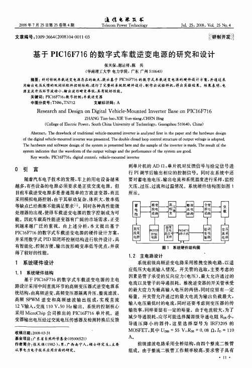
基于PIC16F716的数字式车载逆变电源的研究和设计作者:张天保, 谢运祥, 陈兵作者单位:华南理工大学,电力学院,广东,广州,510640刊名:通信电源技术英文刊名:TELECOM POWER TECHNOLOGIES年,卷(期):2008,25(4)被引用次数:1次1.李强,周席德.车载单相正弦脉宽调制IGBT逆变器的研制[J].电力电子技术.1997,(2):13-15.2.李学海.PIC单片机实用教程[M].北京:航空航天大学出版社.2002.3.Xuejun Pei,Xinehun Lin,etal.Analysis and design of the DSP-based fully digital ControlledUPS.IEEE,Power Electronics.2001,296-300.4.Cha H J.Real-Time digital control of PWM inverter with PI compensator for uninterruptible power supply[C].IEEE IECON Conf.Rec.1990,(2):1125-1128.5.Low K S.A Digital Control Technique for a Single-Phase PWM inverter[M].IEEE TRANSACTIONS ON INDUSTRIAL ELECTRONICS.1998,(8):1335-1340.1.学位论文张天保基于PIC单片机的数字式车载逆变电源的研究与设计2008随着汽车的发展,车上的用电设备越来越多,对车载逆变电源的需求也日益增强,而且有些设备的电源还要求必须是正弦交流电。
但目前国内市场上的车载逆变电源多是普通简单的方波逆变电源,而且采用模拟电路控制,由于其驱动复杂、体积大,效率低等缺点已经渐渐不能满足要求。
同时各种高性能微处理器的出现,使得车载逆变电源的数字控制成为可能。
- 1、下载文档前请自行甄别文档内容的完整性,平台不提供额外的编辑、内容补充、找答案等附加服务。
- 2、"仅部分预览"的文档,不可在线预览部分如存在完整性等问题,可反馈申请退款(可完整预览的文档不适用该条件!)。
- 3、如文档侵犯您的权益,请联系客服反馈,我们会尽快为您处理(人工客服工作时间:9:00-18:30)。
变频器保护和实时监控系统
[摘要]
在现代,人们已经设计和建造出了关于保护和监控直流/交流转换器的系统,该系统是由一个快速反应的硬件保护单元、负载保护装置和自动检测故障发生的逆变器,同时附上一个计算关键操作步骤参数的微控制单元所组成。
文章并不是研究控制装置发生故障的情况。
由硬件结构和模拟传感器组成的控制单元是一个不仅低成本而且稳定可靠的控制单元。
实验结果表明,该实时系统能确保变频器正常运行并且还能监控故障的发生,任何由交流电机驱动的逆变电源都能用此装置来增加系统稳定性,此装置还可用于可再生能源系统中,等等。
一、简介
DC/AC电源逆变器在今天主要用于不间断的供电系统中,例如:感应热量和再生能源系统。
其功能是通过改变电压的幅值和频率将输入进来的直流电压转变成工作需要的交流电压。
这种逆变器的参数规格有输入、输出电压的范围,输出电压频率范围和最大的输出功率。
所以这种逆变器在大小操作系统中运用很广泛。
1. 逆变器一般要求工作在比较严格的环境内,因为经过此种逆变器而输出的的电压、电流会供给对参数变化非常敏感又昂贵的设备。
2. 由于变频器经常在恶劣环境下被运用,所以其本身具有自我保护的功能。
例如:应用在可再生能源和其他案例中关于温度和湿度的敏感变化。
变频器都能在一定的承受范围内正常工作。
3. 随时记录下逆变器的运行过程中的数据变化,假如设备出现故障,此设备都能
将故障原因告知使用者。
考虑到对于逆变器的保护,设计师们通常采用特殊的保护装置和控制电路。
运用最为广泛的保护方式是过电流保护,但是这种方式不是经常都有效,因为保险丝的动作时间太长,动作反应相对缓慢,有时难以起到预想的效果,因此是需要格外配备保护设备的继电器、限流电感。
滤波器具有抑制直流电源和瞬间负载的电压、电流变化引起的高次谐波的能力,同时它的缺点是会增加逆变器的功率损耗,和设备的成本、重量。
电源逆变器有内在的过流保护功能,能适当设计成与直流电感连接来构成过载保护的条件。
电压源逆变器(逆变器)包括一个滤波器的输出阶段,因此有一个输出短路条件的限制,这个限制称为输出滤波电感的电流上升率。
在前面的情况下,在高电感的情况下会导致逆变器损耗增加。
如果上述任何数量的超过预定的限制,将会产生一个由直流电源供应的驱动电机关闭的信号,将会影响到直流电源的输出。
在电机驱动应用中,变频器通常只用作过载保护或者作为一种使用侵入电流传感技术来起作用,用它来测量直流电流或负载电流或特殊电机控制算法技术。
然而,上述方法的实施都是在没有充分检测所有可能发生故障的情况下执行的,例如:一种直流环节中关于电容短路的电路。
如下图所示:
图1 关于电容短路电路图
先进的单片机技术已经领导着监控数字控制技术和控制逆变器的发展,利用卡门滤波器来监控输出电压的幅度和频率,这种的技术已经记载在参考文献[12]中。
虽然这种方式具有将一定数目的控制功能整合到单独一个芯片上的优势,但是其并不保护逆变器抵御所有故障的发生。
如果这种方式扩展应用到更重要的信号检测中,系统将不会很迅速的保护逆变器来应对发生的故障;相反就需要更快的微控制器或者数字信号处理器(TMS)来保护逆变器,但这同样会增加系统成本。
对于检测一个逆变器是否发生故障,现在已经提出了好几种方法,例如一种检测电源开关是否发生故障的诊断系统,它是一个由脉宽调制逆变器供电的同步电流传感器,这部分资料在参考文献[13]上体现,这是在分析电流适量轨迹和瞬时频率
的基础上得到的故障模式。
由专家分析出来的故障诊断系统是基于逆变器的实时监控的并在参考文献[14]上体现,上述提到的方法旨在帮助系统在出现故障后排除故障原因。
在上述的所有方法中可以得到的是大部分逆变器是不完全履行先前逆变电源要求的执行步骤(步骤1-3)。
在本文中,用来保护和监控直流/交流逆变器的低成本控制单元将会被介绍。
该系统是由以下几个部件组成的:
(一)硬件保护单元,在逆变器电路特定点得到的比较适当信号会与预定水平的信号相比较,以便确定最适合系统的信号来执行正确系统操作。
;
(二)一个基于控制器的实时系统监测着逆变器操作时的所有关键参数的变化。
当系统发生故障时,保护装置中的硬件部分会立即启动确保逆变器万无一失,与此同时微控制单元会立即通知操作员系统发生故障。
微控制器单元会通过遥感—232协议来与计算机进行通信。
这些必要的变频器参数是基于微控制器的实现并衡量非侵入性和非耗散型操作来确定的。
一般首选的更快的处理器是由于其较低的成本。
然而,一个数字信号处理器将作为一个附加的实现数字化的控制功能模块(即功率半导体控制器,其带有先进的电池检测算法,等等),在这篇文章中并不针对研究控制单元发生的障碍。
这篇论文的组织结构如下:变频器的硬件发生故障的原因解释记录在第2节;关于传感器和驱动器时间和力量上的检测问题在第3节里解释;第4节里提出控制和监控单位;微控制器单元的算法分析在第5节,同时结果在第6节。
二、逆变器硬件结构和故障原因
一般通用逆变器的结构图如图2所示。
建立在IGBT桥梁调节得到的直流输入电压为正弦脉宽调制波,低通滤波器,LC型过滤器是用来调制解调输出(220V、50HZ)正弦波形,而电源变压器是用于生产低失真输出所需的高电压,另外,电源功率的大小取决于逆变器功率和直流输入电压值理想效率。
逆变器操作过程中可能出现的问题在下方列出:
1.经过输入电压输出的逆变器的规格
2.电路超载时的情况
3.瞬时变化的输出电压,例如,连接和断开电机时的瞬间电压
4.电路短路时的输出状况
5.逆变器输出的电压和频率规格
6.在高温环境下,半导体特性的变化
7.高湿度环境可能影响电子器件的动作
8.其他突发因素影响,例如逆变器的驱动电路发生故障,等
如果上述任意一种问题发生,逆变器必须立即停止运行来保护负载和逆变器电源免遭破坏,同时系统管理者必须得到关于这个问题的相关资料。
平均发生故障的间隔时间(平均无故障)是正常工作时间几万倍。
三、传感器
该传感器在逆变器的显示图如下图所示3.霍尔传感器用于测量直流输入电流和交流输出电流。
他们有较好的分流电阻,如从主电源电路独立地隔离出灰尘、湿
度及时间等特征,此外,
它们还具有频率带宽的特点,包括低温变化下的直流操作变化特点,所以他们是理想的电流检测逆变器。
无反馈的霍尔效应传感器能保证低功耗。
但是,因为反应速度比较缓慢,所以在过流的情况下不能有效保护功率半导体。
因此,过流保护电路一般都采用组组并联的场效应管,如下图所示
图3 传感器在逆变电路的显示图
四、结论
这种低成本、实时控制装置的开发,它能有效地保护和检测直流/交流逆变器,该系统的目标是在确保逆变器输出电压下降为零的情况(也就是无故障、安全的情况);当操作不当时,控制单元就会发生故障,再将故障发生的情况和关键参数细节会传递给系统管理者,此系统的设计是基于高性能的单片机和现成的电子元件,利用实验模拟出控制单元的模型,并在实验室内构建和测试最贴合系统的正弦脉宽调制逆变器。
实验结果证明:该系统保证了变频器的正常使用和确保故障发生时的安全操作。
该装置能增加系统的可靠性,由交流电机驱动的任何电源变频器和可再生能源系统,等等。
在后一种情况下电池的充电和交流/直流转换器的监测中包括现有的微控制器算法、先进的电池检测算法和数字脉宽调制逆变器技术,所以,在今后这种系统会在更广阔的领域中被使用。