XC7A100T-FGG676I FPGA设计小结
FPGA可编程逻辑器件芯片XC7A100T-2FGG484C中文规格书
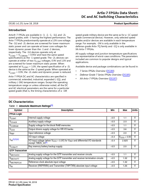
IntroductionArtix®-7 FPGAs are available in -3, -2, -1, -1LI, and -2L speed grades, with -3 having the highest performance. The Artix-7FPGAs predominantly operate at a 1.0V core voltage. The -1LI and -2L devices are screened for lower maximum static power and can operate at lower core voltages for lower dynamic power than the -1 and -2 devices, respectively. The -1LI devices operate only atV CCINT=V CCBRAM=0.95V and have the same speed specifications as the -1 speed grade. The -2L devices can operate at either of two V CCINT voltages, 0.9V and 1.0V and are screened for lower maximum static power. When operated at V CCINT=1.0V, the speed specification of a -2L device is the same as the -2 speed grade. When operated at V CCINT=0.9V, the -2L static and dynamic power is reduced. Artix-7 FPGA DC and AC characteristics are specified in commercial, extended, industrial, expanded (-1Q), and military (-1M) temperature ranges. Except the operating temperature range or unless otherwise noted, all the DC and AC electrical parameters are the same for a particular speed grade (that is, the timing characteristics of a -1M speed grade military device are the same as for a -1C speed grade commercial device). However, only selected speed grades and/or devices are available in each temperature range. For example, -1M is only available in the defense-grade Artix-7Q family and -1Q is only available in XA Artix-7FPGAs.All supply voltage and junction temperature specifications are representative of worst-case conditions. The parameters included are common to popular designs and typical applications.Available device and package combinations can be found in:•7Series FPGAs Overview (DS180)•Defense-Grade 7Series FPGAs Overview (DS185)•XA Artix-7 FPGAs Overview (DS197)DC CharacteristicsArtix-7 FPGAs Data Sheet: DC and AC Switching CharacteristicsDS181 (v1.25) June 18, 2018Product SpecificationTable 1:Absolute Maximum Ratings(1)Symbol Description Min Max Units FPGA LogicV CCINT Internal supply voltage–0.5 1.1VV CCAUX Auxiliary supply voltage–0.5 2.0VV CCBRAM Supply voltage for the block RAM memories–0.5 1.1VV CCO Output drivers supply voltage for HR I/O banks–0.5 3.6VV REF Input reference voltage–0.5 2.0VV IN(2)(3)(4)I/O input voltage–0.4V CCO+0.55V I/O input voltage (when V CCO=3.3V) for V REF and differential I/O standardsexcept TMDS_33(5)–0.4 2.625VV CCBATT Key memory battery backup supply–0.5 2.0V GTP TransceiverV MGTAVCC Analog supply voltage for the GTP transmitter and receiver circuits–0.5 1.1V V MGTAVTT Analog supply voltage for the GTP transmitter and receiver termination circuits–0.5 1.32V V MGTREFCLK Reference clock absolute input voltage–0.5 1.32V V IN Receiver (RXP/RXN) and Transmitter (TXP/TXN) absolute input voltage–0.5 1.26VVersion In:Typical V CCINTDeviceISE 14.7Vivado 2018.2(Table2)N/A 1.22 1.0V XC7A12T, XC7A15T, XC7A25T, XC7A35T, XC7A50T, XC7A75TN/A 1.220.95V XC7A12T, XC7A15T, XC7A25T, XC7A35T, XC7A50T, XC7A75T, XC7A100T,XC7A200TN/A 1.140.9V XC7A12T, XC7A15T, XC7A25T, XC7A35T, XC7A50T, XC7A75T1.10 1.22 1.0V XC7A100T, XC7A200T1.07 1.140.9V XC7A100T, XC7A200TN/A 1.15 1.0V XA7A12T, XA7A15T, XA725T, XA7A35T, XA7A50T, XA7A75T1.07 1.15 1.0V XA7A100T1.06 1.11 1.0V XQ7A100T, XQ7A200TN/A 1.11 1.0V XQ7A50TDeviceSpeed Grade1.0V0.95V0.9V -3-2-2LE-1-1Q-1M-1LI-2LEXC7A12T Vivado tools2018.2 v1.22Vivado tools 2017.4 v1.20N/A N/A Vivado tools2017.4 v1.20Vivado tools2018.1 v1.14XC7A15T Vivado tools 2014.4 v1.14N/A N/A Vivado tools2014.4 v1.14Vivado tools 2014.4 v1.10XC7A25T Vivado tools2018.2 v1.22Vivado tools 2017.4 v1.20N/A N/A Vivado tools2017.4 v1.20Vivado tools2018.1 v1.14XC7A35T Vivado tools 2013.4 v1.11N/A N/A Vivado tools2014.4 v1.14Vivado tools 2013.4 v1.08Selecting the Correct Speed Grade and Voltage in the Vivado ToolsIt is important to select the correct device speed grade and voltage in the Vivado tools for the device that you are selecting.To select the 1.0V speed specifications in the Vivado tools, select the Artix-7, XA Artix-7, or Defense Grade Artix-7Q sub-family, and then select the part name that is the device name followed by the package name followed by the speed grade. For example, select the xc7a100tfgg676-3 part name for the XC7A100T device in the FGG676 package and -3 (1.0V) speed grade or select the xc7a100tfgg676-2L part name for the XC7A100T device in the FGG676 package and -2LE (1.0V) speed grade.To select the -1LI (0.95V) speed specifications in the Vivado tools, select the Artix-7 sub-family and then select the part name that is the device name followed by an “i” followed by the package name followed by the speed grade. For example, select the xc7a100tifgg676-1L part name for the XC7A100T device in the FGG676 package and -1LI (0.95V) speed grade. The -1LI (0.95V) speed specifications are not supported in the ISE tools.To select the -2LE (0.9V) speed specifications in the Vivado tools, select the Artix-7 Low Voltage sub-family and then select the part name that is the device name followed by an “l” followed by the package name followed by the speed grade. For example, select the xc7a100tlfgg676-2L part name for the XC7A100T device in the FGG676 package and -2LE (0.9V) speed grade.XC7A50T Vivado tools 2013.4 v1.11N/A N/A Vivado tools 2014.4 v1.14Vivado tools 2013.4 v1.08XC7A75T Vivado tools 2013.3 v1.10N/A N/A Vivado tools 2014.4 v1.14Vivado tools 2013.3 v1.07XC7A100T ISE tools 14.4 or Vivado tools 2012.4 with the14.4/2012.4 device pack v1.07N/A N/A Vivado tools 2014.4 v1.14ISE tools 14.5 or Vivado tools 2013.1 v1.05XC7A200T ISE tools 14.4 or Vivado tools 2012.4 with the14.4/2012.4 device pack v1.07N/AN/A Vivado tools 2014.4 v1.14XA7A12T N/A Vivado tools 2018.1 v1.15N/A Vivado tools 2018.1 v1.15N/A N/A N/A XA7A15T N/A Vivado tools 2014.4 v1.14N/A Vivado tools 2014.4 v1.14N/A N/A N/A XA7A25T N/A Vivado tools 2018.1 v1.15N/A Vivado tools 2018.1 v1.15N/A N/A N/A XA7A35T N/A Vivado tools 2014.1 v1.09N/A Vivado tools 2014.1 v1.09N/A N/A N/A XA7A50T N/A Vivado tools 2014.1 v1.09N/A Vivado tools 2014.1 v1.09N/A N/A N/A XA7A75T N/A Vivado tools 2014.1 v1.09N/A Vivado tools 2014.1 v1.09N/A N/A N/A XA7A100TN/AISE tools 14.5 or Vivado tools 2013.1 v1.05N/AISE tools 14.5 or Vivado tools 2013.1 v1.05ISE tools 14.6 or Vivado tools2013.2 v1.06N/AN/AN/AXQ7A50T N/A Vivado tools 2014.2 v1.08N/A Vivado tools2014.2 v1.08N/A Vivado tools 2014.2 v1.08Vivado tools 2015.4 v1.11N/A XQ7A100TN/AISE tools 14.5 or Vivado tools 2013.1 v1.04N/AISE tools 14.5 or Vivado tools 2013.1 v1.04N/AISE tools 14.6 or Vivado tools 2013.2 v1.05Vivado tools 2015.4 v1.11N/AXQ7A200T N/A ISE tools 14.5 or Vivado tools 2013.1 v1.04N/A ISE tools 14.5 or Vivado tools 2013.1 v1.04N/A ISE tools 14.6 or Vivado tools 2013.2 v1.05Vivado tools 2015.4 v1.11N/ATable 14:Artix-7 Device Production Software and Speed Specification Release (Cont’d)DeviceSpeed Grade1.0V0.95V0.9V -3-2-2LE-1-1Q -1M -1LI -2LEDescriptionSpeed GradeUnits1.0V0.95V0.9V-3-2/-2LE-1-1LI-2LESDR LVDS transmitter (using OSERDES; DATA_WIDTH=4 to 8)680680600600600Mb/s DDR LVDS transmitter (using OSERDES; DATA_WIDTH=4 to 14)12501250950950950Mb/s SDR LVDS receiver (SFI-4.1)(1)680680600600600Mb/s DDR LVDS receiver (SPI-4.2)(1)12501250950950950Mb/sMemory StandardSpeed GradeUnits1.0V0.95V0.9V-3-2/-2LE-1-1Q/-1M-1LI-2LE4:1 Memory ControllersDDR31066(3)800800667800800Mb/s DDR3L800800667N/A667667Mb/s DDR2800800667533667667Mb/s 2:1 Memory ControllersDDR3800700620620620620Mb/s DDR3L800700620N/A620620Mb/s DDR2800700620533620620Mb/s LPDDR2667667533400533533Mb/s。
FPGA可编程逻辑器件芯片XC7A200T-1FBG676I中文规格书

XTP385 (v2.0) March 30, 2015OverviewTo ensure business continuity and enable high volume supply chain capabilities for all Virtex®-6 and selected 7 series FPGAs product families, Xilinx is qualifying an additional substrate supplier, Unimicron Technology Corporation (UMTC) for flip chip ball grid area (FCBGA) packages.For Virtex-6 FPGAs, this change affects all standard and specification control document (SCD) XC Commercial (C) and Industrial (I) grade devices. Hi-Rel “XQ” devices are not affected by this PCN.For Artix®-7, Zynq®-7000 All Programmable, Virtex®-7 and Kintex®-7 in the SB, FB, FF, SBG, FBG and FFG packages, this change affects all standard and specification control document (SCD) XC Commercial (C) grade, Extended (E) grade and Industrial (I) grade devices. Virtex-7 in the FL, FLG, FH and FHG packages, and Automotive “XA” devices for 7 series FPGAs are not affected by this PCN. Kintex®-7Q, Virtex®-7Q and Zynq®-7000Q All Programmable Hi-Rel “XQ” FPGAs RF flip chip packages are affected (Refer to XCN14013).This additional supplier will adhere to the same performance, quality and reliability specifications that apply to all product families proven through extensive qualification and testing. As a result, there is no change in form, fit, function, or reliability with this substrate supplier addition.FAQsQ: What is the change?Xilinx is qualifying an additional substrate supplier, Unimicron Technology Corporation (UMTC) for flip chip ball grid area (FCBGA) packages for all Virtex-6 and selected 7 series FPGAs product families. UMTC is a reputablecompany supplying component substrate and system printed circuit board to many semiconductor customers and original equipment make (OEM) customers for over 10 years. Q: Why is Xilinx making this change?This change ensures business continuity and enables high volume supply chain capabilities for Xilinx product families.Q: Why adding Phase 3?As a result of the successful implementation for Xilinx FPGAs (Virtex-6 FPGAs and 7-series), we are expanding this program to include SoC (Zynq-7000 All Programmable) to this change. Q: Which products are affected?For Virtex-6 FPGAs, this change affects all standard and specification control document (SCD) XC Commercial (C) and Industrial (I) grade devices. Hi-Rel “XQ” devices in the FFG1156 package are not affected by this PCN. For Artix-7, Zynq-7000 All Programmable, Virtex-7 and Kintex-7 in the SB, FB, FF, SBG, FBG and FFG packages, this change affects all standard and specification control document (SCD) XC Commercial (C) grade, Extended (E) grade and Industrial (I) grade devices. Virtex-7 in the FL, FLG, FH and FHG packages, and Automotive“XA” devices找FPGA ,上赛灵思半导体(深圳)有限公司FAQ: Transition Schedule for Substrate Supplier for Virtex-6 and 7 Series FPGAs Flip Chip PackagesXTP385 (v2.0) March 30, 2015for 7 series FPGAs are not affected by this PCN. Kintex-7Q, Virtex-7Q and Zynq-7000Q All Programmable Hi-Rel “XQ” FPGAs RF flip chip packages are affected (Refer to XCN14013).Affected device package-pin are listed in the Table 1, Table 2, Table 3, Table 4 and Table 5 below:FAQ: Transition Schedule for Substrate Supplier for Virtex-6 and 7 Series FPGAs Flip Chip PackagesXTP385 (v2.0) March 30, 2015Table 5: Zynq-7000 FPGAs Devices Package Product AffectedNotes:(1)Please refer to Table 6 Phase 1 cross-ship schedule (2)Please refer to Table 7 Phase 2 cross-ship schedule (3)Please refer to Table 8 Phase 3 cross-ship schedule*For inquiries about a specific part number, please contact your customer operations representative or CQE representative for any additional questions.Q: When will this change take effect?This change will take effect in Q1, CY2015. At that time, Xilinx will start cross shipping all Virtex-6 product families and selected 7 series FPGAs product families from UMTC. This will result in initial production device shipments to customers in the timelines indicated in Table 6 and Table 7 and Table 8 below.Table 6: Phase 1 - Virtex-6 and Kintex-7 Devices Qualification Completion and Cross-Ship ScheduleFAQ: Transition Schedule for Substrate Supplier for Virtex-6 and 7 Series FPGAs Flip Chip PackagesXTP385 (v2.0) March 30, 2015FAQ: Transition Schedule for Substrate Supplier for Virtex-6 and 7 Series FPGAs Flip Chip PackagesXTP385 (v2.0) March 30, 2015Revision HistoryThe following table shows the revision history for this document:。
FPGA可编程逻辑器件芯片XC7K160T-2FFG676I中文规格书

7Series FPGAs Data Sheet: OverviewSpartan-7 FPGA Feature SummaryTable 2:Spartan-7 FPGA Feature Summary by DeviceDevice LogicCellsCLBDSPSlices(2)Block RAM Blocks(3)CMTs(4)PCIe GT XADCBlocksTotal I/OBanks(5)Max UserI/O Slices(1)MaxDistributedRAM (Kb)18Kb36Kb Max(Kb)XC7S66,000938701010518020002100 XC7S1512,8002,00015020201036020002100 XC7S2523,3603,6503138090451,62030013150 XC7S5052,1608,150600120150752,70050015250 XC7S7576,80012,000832140180903,24080018400 XC7S100102,40016,0001,1001602401204,32080018400 Notes:1.Each 7series FPGA slice contains four LUTs and eight flip-flops; only some slices can use their LUTs as distributed RAM or SRLs.2.Each DSP slice contains a pre-adder, a 25x18 multiplier, an adder, and an accumulator.3.Block RAMs are fundamentally 36Kb in size; each block can also be used as two independent 18Kb blocks.4.Each CMT contains one MMCM and one PLL.5.Does not include configuration Bank 0.Table 3:Spartan-7 FPGA Device-Package Combinations and Maximum I/OsPackage CPGA196CSGA225CSGA324FTGB196FGGA484FGGA676Size (mm)8 x 813 x 1315 x 1515 x 1523 x 2327 x 27Ball Pitch(mm)0.50.80.8 1.0 1.0 1.0 Device HR I/O(1)HR I/O(1)HR I/O(1)HR I/O(1)HR I/O(1)HR I/O(1)XC7S6100100100XC7S151********XC7S25150150100XC7S50210100250XC7S75338400XC7S100338400Notes:1.HR = High-range I/O with support for I/O voltage from 1.2V to 3.3V.Encryption, Readback, and Partial ReconfigurationIn all 7series FPGAs (except XC7S6 and XC7S15), the FPGA bitstream, which contains sensitive customer IP, can be protected with 256-bit AES encryption and HMAC/SHA-256 authentication to prevent unauthorized copying of the design. The FPGA performs decryption on the fly during configuration using an internally stored 256-bit key. This key can reside in battery-backed RAM or in nonvolatile eFUSE bits.Most configuration data can be read back without affecting the system's operation. Typically, configuration is anall-or-nothing operation, but Xilinx 7series FPGAs support partial reconfiguration. This is an extremely powerful and flexible feature that allows the user to change portions of the FPGA while other portions remain static. Users can time-slice these portions to fit more IP into smaller devices, saving cost and power. Where applicable in certain designs, partial reconfiguration can greatly improve the versatility of the FPGA.XADC (Analog-to-Digital Converter)Highlights of the XADC architecture include:•Dual 12-bit 1MSPS analog-to-digital converters (ADCs)•Up to 17 flexible and user-configurable analog inputs•On-chip or external reference option•On-chip temperature (±4°C max error) and power supply (±1% max error) sensors•Continuous JTAG access to ADC measurementsAll Xilinx 7series FPGAs (except XC7S6 and XC7S15) integrate a new flexible analog interface called XADC. When combined with the programmable logic capability of the 7series FPGAs, the XADC can address a broad range of data acquisition and monitoring requirements. For more information, go.The XADC contains two 12-bit 1 MSPS ADCs with separate track and hold amplifiers, an on-chip analog multiplexer (up to 17external analog input channels supported), and on-chip thermal and supply sensors. The two ADCs can be configured to simultaneously sample two external-input analog channels. The track and hold amplifiers support a range of analog input signal types, including unipolar, bipolar, and differential. The analog inputs can support signal bandwidths of at least500KHz at sample rates of 1MSPS. It is possible to support higher analog bandwidths using external analog multiplexer mode with the dedicated analog input (see UG480, 7 Series FPGAs and Zynq-7000 All Programmable SoC XADC Dual 12-Bit 1 MSPS Analog-to-Digital Converter User Guide).The XADC optionally uses an on-chip reference circuit (±1%), thereby eliminating the need for any external active components for basic on-chip monitoring of temperature and power supply rails. To achieve the full 12-bit performance of the ADCs, an external 1.25V reference IC is recommended.If the XADC is not instantiated in a design, then by default it digitizes the output of all on-chip sensors. The most recent measurement results (together with maximum and minimum readings) are stored in dedicated registers for access at any time via the JTAG interface. User-defined alarm thresholds can automatically indicate over-temperature events and unacceptable power supply variation. A user-specified limit (for example, 100°C) can be used to initiate an automatic powerdown.EasyPath-7 FPGAsEasyPath-7 FPGAs provide a fast, simple, and risk-free solution for cost reducing Kintex-7, Virtex-7 T, and Virtex-7 XT FPGA designs. EasyPath-7 FPGAs support the same packages, speed grades, and match all Kintex-7 or Virtex-7 FPGA data sheet specifications (in function and timing). With no re-engineering or re-qualification, EasyPath-7 FPGAs deliver the lowest total product cost compared to any other FPGA cost-reduction solution.7Series FPGA Ordering InformationTable12 shows the speed and temperature grades available in the different device families. Some devices might not be available in every speed and temperature grade.Table 12:7 Series Speed Grade and Temperature RangesDevice Family DevicesSpeed Grade, Temperature Range, and Operating VoltageCommercial (C)0°C to +85°CExtended (E)0°C to +100°CIndustrial (I)–40°C to +100°CExpanded (Q)–40°C to +125°CSpartan-7All -2C (1.0V)-2I (1.0V)-1C (1.0V)-1I (1.0V)-1Q (1.0V)-1LI (0.95V)Artix-7All-3E (1.0V)-2C (1.0V)-2I (1.0V)-2LE (1.0V or 0.9V)-1C (1.0V)-1I (1.0V)-1LI (0.95V)Kintex-7XC7K70T-3E (1.0V)-2C (1.0V)-2I (1.0V)-2LE (1.0V or 0.9V)-1C (1.0V)-1I (1.0V) XC7K160TXC7K325TXC7K355TXC7K410TXC7K420TXC7K480T-3E (1.0V)-2C (1.0V)-2I (1.0V)-2LE (1.0V or 0.9V)-2LI (0.95V)-1C (1.0V)-1I (1.0V)Virtex-7 TXC7V585T-3E (1.0V)-2C (1.0V)-2I (1.0V)-2LE (1.0V)-1C (1.0V)-1I (1.0V) XC7V2000T-2C (1.0V)-2GE (1.0V)-2LE (1.0V)-1C (1.0V)-1I (1.0V)Virtex-7 XTXC7VX330TXC7VX415TXC7VX485TXC7VX550TXC7VX690T-3E (1.0V)-2C (1.0V)-2I (1.0V)-2LE (1.0V)-1C (1.0V)-1I (1.0V) XC7VX980T-2C (1.0V)-2LE (1.0V)-1C (1.0V)-1I (1.0V) XC7VX1140T-2C (1.0V)-2GE (1.0V)-2LE (1.0V)-1C (1.0V)-1I (1.0V)Virtex-7 HT All -2C (1.0V)-2GE (1.0V)-2LE (1.0V) -1C (1.0V)。
XC7A100T-FGG676I FPGA设计小结教学内容

X C7A100T-F G G676IF PG A设计小结XC7A100T-FGG676I FPGA设计小结XC7A100T-FGG676I是XILINX 的Artix-7 Family FPGA,具有高性价比,低功耗能,小封装等优点。
在4P项目中作为FPGA主要实现不同接口的报文桥接功能。
XC7A100T-FGG676I基本配置XC7A100T-FGG676I在本项目中用于Master SPI模式,基本配置如下,具体请见文件ug470XC7A100T-FGG676I的电源设计以及功耗XC7A100T-FGG676I电源主要有1.0V,1.2V,1.8V,3.3V,由于项目中使用的是DDR3,故和DDR3相连的FPGA的BANK16的VCCO使用的是1.5V。
本项目中的FPGA is available in -2 speed grades ,故VCCINT=1.0V。
根据XC7A100T-FGG676I的要求,为了减少电流消耗和确保上电的时候三态,电源上电顺序:1.0>1.2>1.8>3.3/1.5VXC7A100T-FGG676I上没有BANK12和BANK33,据FAE反馈这些BANK其实里面是不接到硅片上的。
它们只是为管脚兼容做的。
故这些管脚悬空接地接电源都可以。
为方便走线计,建议悬空,VCCO_12和VCC_33 pin脚悬空:FPGA和DDR3设计XC7A100T-FGG676I的BANK16基本没有复用脚,故BANK16和DDR3相连。
BANK16的VCCO连接到1.5V(其他BANK的VCCO连接到3.3V)。
本项目要求1G/2G DDR3相互兼容,故预留了一个DDR3_A13,注意选择的IO口要在一个time group中,XC7A100T-FGG676I和DDR3连接时,DDR3的LDM和UDM需要接地。
Note:1)、某些总线在不使用Phase的情况下,是可以使用不在同一个time group,2)、查看FPGA每个BANK的pin定义,发现H17,E22等,纯粹作为IO口使用,不在任何的time group中,对此IO需注意。
FPGA可编程逻辑器件芯片XC7K160T-1FFG676I中文规格书

General DescriptionXilinx® 7series FPGAs comprise four FPGA families that address the complete range of system requirements, ranging from low cost, small form factor, cost-sensitive, high-volume applications to ultra high-end connectivity bandwidth, logic capacity, and signal processing capability for the most demanding high-performance applications. The 7series FPGAs include:•Spartan®-7 Family: Optimized for low cost, lowest power, and high I/O performance. Available in low-cost, very small form-factorpackaging for smallest PCB footprint.•Artix®-7 Family: Optimized for low power applications requiring serial transceivers and high DSP and logic throughput. Provides the lowest total bill of materials cost for high-throughput, cost-sensitiveapplications.•Kintex®-7 Family: Optimized for best price-performance with a 2X improvement compared to previous generation, enabling a new class of FPGAs.•Virtex®-7 Family: Optimized for highest system performance and capacity with a 2X improvement in system performance. Highestcapability devices enabled by stacked silicon interconnect (SSI)technology.Built on a state-of-the-art, high-performance, low-power (HPL), 28nm, high-k metal gate (HKMG) process technology, 7series FPGAs enable an unparalleled increase in system performance with 2.9Tb/s of I/O bandwidth, 2 million logic cell capacity, and 5.3TMAC/s DSP, while consuming 50% less power than previous generation devices to offer a fully programmable alternative to ASSPs and ASICs.Summary of 7Series FPGA Features•Advanced high-performance FPGA logic based on real 6-input look-up table (LUT) technology configurable as distributed memory.•36Kb dual-port block RAM with built-in FIFO logic for on-chip data buffering.•High-performance SelectIO™ technology with support for DDR3 interfaces up to 1,866 Mb/s.•High-speed serial connectivity with built-in multi-gigabit transceivers from 600Mb/s to max. rates of 6.6Gb/s up to 28.05Gb/s, offering a special low-power mode, optimized for chip-to-chip interfaces.• A user configurable analog interface (XADC), incorporating dual 12-bit 1MSPS analog-to-digital converters with on-chip thermal and supply sensors.•DSP slices with 25x18 multiplier, 48-bit accumulator, and pre-adder for high-performance filtering, including optimized symmetriccoefficient filtering.•Powerful clock management tiles (CMT), combining phase-locked loop (PLL) and mixed-mode clock manager (MMCM) blocks for high precision and low jitter.•Quickly deploy embedded processing with MicroBlaze™ processor.•Integrated block for PCI Express® (PCIe), for up to x8 Gen3 Endpoint and Root Port designs.•Wide variety of configuration options, including support for commodity memories, 256-bit AES encryption with HMAC/SHA-256 authentication, and built-in SEU detection and correction.•Low-cost, wire-bond, bare-die flip-chip, and high signal integrity flip-chip packaging offering easy migration between family members in the same package. All packages available in Pb-free and selected packages in Pb option.•Designed for high performance and lowest power with 28nm, HKMG, HPL process, 1.0V core voltage process technology and0.9V core voltage option for even lower power.7Series FPGAs Data Sheet: Overview DS180 (v2.6) February 27, 2018Product SpecificationTable 1:7Series Families ComparisonMax. Capability Spartan-7Artix-7Kintex-7Virtex-7Logic Cells102K215K478K1,955KBlock RAM(1) 4.2Mb13Mb34Mb68MbDSP Slices 1607401,9203,600DSP Performance(2)176 GMAC/s929GMAC/s2,845GMAC/s5,335GMAC/s MicroBlaze CPU(3)260 DMIPs303 DMIPs438 DMIPs441 DMIPs Transceivers–163296Transceiver Speed– 6.6Gb/s12.5Gb/s28.05Gb/sSerial Bandwidth–211Gb/s800Gb/s2,784Gb/sPCIe Interface–x4 Gen2x8 Gen2x8 Gen3Memory Interface800Mb/s1,066Mb/s1,866Mb/s1,866Mb/sI/O Pins400500500 1,200I/O Voltage 1.2V–3.3V 1.2V–3.3V 1.2V–3.3V 1.2V–3.3VPackage Options Low-Cost, Wire-Bond Low-Cost, Wire-Bond,Bare-Die Flip-Chip Bare-Die Flip-Chip and High-Performance Flip-ChipHighest PerformanceFlip-ChipNotes:1.Additional memory available in the form of distributed RAM.2.Peak DSP performance numbers are based on symmetrical filter implementation.3.Peak MicroBlaze CPU performance numbers based on microcontroller preset.Mixed-Mode Clock Manager and Phase-Locked LoopThe MMCM and PLL share many characteristics. Both can serve as a frequency synthesizer for a wide range of frequencies and as a jitter filter for incoming clocks. At the center of both components is a voltage-controlled oscillator (VCO), which speeds up and slows down depending on the input voltage it receives from the phase frequency detector (PFD).There are three sets of programmable frequency dividers: D, M, and O. The pre-divider D (programmable by configuration and afterwards via DRP) reduces the input frequency and feeds one input of the traditional PLL phase/frequency comparator. The feedback divider M (programmable by configuration and afterwards via DRP) acts as a multiplier because it divides the VCO output frequency before feeding the other input of the phase comparator. D and M must be chosen appropriately to keep the VCO within its specified frequency range. The VCO has eight equally-spaced output phases (0°, 45°, 90°, 135°, 180°, 225°, 270°, and 315°). Each can be selected to drive one of the output dividers (six for the PLL, O0 to O5, and seven for the MMCM, O0 to O6), each programmable by configuration to divide by any integer from 1 to 128. The MMCM and PLL have three input-jitter filter options: low bandwidth, high bandwidth, or optimized mode. Low-bandwidth mode has the best jitter attenuation but not the smallest phase offset. High-bandwidth mode has the best phase offset, but not the best jitter attenuation. Optimized mode allows the tools to find the best setting.MMCM Additional Programmable FeaturesThe MMCM can have a fractional counter in either the feedback path (acting as a multiplier) or in one output path. Fractional counters allow non-integer increments of 1/8 and can thus increase frequency synthesis capabilities by a factor of 8.The MMCM can also provide fixed or dynamic phase shift in small increments that depend on the VCO frequency. At 1600MHz, the phase-shift timing increment is 11.2ps.Clock DistributionEach 7series FPGA provides six different types of clock lines (BUFG, BUFR, BUFIO, BUFH, BUFMR, and the high-performance clock) to address the different clocking requirements of high fanout, short propagation delay, and extremely low skew.Global Clock LinesIn each 7series FPGA (except XC7S6 and XC7S15), 32 global clock lines have the highest fanout and can reach every flip-flop clock, clock enable, and set/reset, as well as many logic inputs. There are 12 global clock lines within any clock region driven by the horizontal clock buffers (BUFH). Each BUFH can be independently enabled/disabled, allowing for clocks to be turned off within a region, thereby offering fine-grain control over which clock regions consume power. Global clock lines can be driven by global clock buffers, which can also perform glitchless clock multiplexing and clock enable functions. Global clocks are often driven from the CMT, which can completely eliminate the basic clock distribution delay.Regional ClocksRegional clocks can drive all clock destinations in their region. A region is defined as an area that is 50 I/O and 50 CLB high and half the chip wide. 7series FPGAs have between two and twenty-four regions. There are four regional clock tracks in every region. Each regional clock buffer can be driven from any of four clock-capable input pins, and its frequency can optionally be divided by any integer from 1 to 8.I/O ClocksI/O clocks are especially fast and serve only I/O logic and serializer/deserializer (SerDes) circuits, as described in theI/O Logic section. The 7series devices have a direct connection from the MMCM to the I/O for low-jitter, high-performance interfaces.Block RAMSome of the key features of the block RAM include:•Dual-port 36Kb block RAM with port widths of up to 72•Programmable FIFO logic•Built-in optional error correction circuitryEvery 7series FPGA has between 5 and 1,880 dual-port block RAMs, each storing 36Kb. Each block RAM has two completely independent ports that share nothing but the stored data.Synchronous OperationEach memory access, read or write, is controlled by the clock. All inputs, data, address, clock enables, and write enables are registered. Nothing happens without a clock. The input address is always clocked, retaining data until the next operation. An optional output data pipeline register allows higher clock rates at the cost of an extra cycle of latency.During a write operation, the data output can reflect either the previously stored data, the newly written data, or can remain unchanged.Programmable Data WidthEach port can be configured as 32K×1, 16K×2, 8K×4, 4K×9 (or8), 2K×18 (or16), 1K×36 (or32), or 512×72 (or64). The two ports can have different aspect ratios without any constraints.Each block RAM can be divided into two completely independent 18Kb block RAMs that can each be configured to any aspect ratio from 16K×1 to 512×36. Everything described previously for the full 36Kb block RAM also applies to each of the smaller 18Kb block RAMs.Only in simple dual-port (SDP) mode can data widths of greater than 18bits (18Kb RAM) or 36bits (36Kb RAM) be accessed. In this mode, one port is dedicated to read operation, the other to write operation. In SDP mode, one side (read or write) can be variable, while the other is fixed to 32/36 or 64/72.Both sides of the dual-port 36Kb RAM can be of variable width.Two adjacent 36Kb block RAMs can be configured as one cascaded 64K×1 dual-port RAM without any additional logic. Error Detection and CorrectionEach 64-bit-wide block RAM can generate, store, and utilize eight additional Hamming code bits and perform single-bit error correction and double-bit error detection (ECC) during the read process. The ECC logic can also be used when writing to or reading from external 64- to 72-bit-wide memories.FIFO ControllerThe built-in FIFO controller for single-clock (synchronous) or dual-clock (asynchronous or multirate) operation increments the internal addresses and provides four handshaking flags: full, empty, almost full, and almost empty. The almost full and almost empty flags are freely programmable. Similar to the block RAM, the FIFO width and depth are programmable, but the write and read ports always have identical width.First word fall-through mode presents the first-written word on the data output even before the first read operation. After the first word has been read, there is no difference between this mode and the standard mode.7Series FPGA Ordering InformationTable12 shows the speed and temperature grades available in the different device families. Some devices might not be available in every speed and temperature grade.Table 12:7 Series Speed Grade and Temperature RangesDevice Family DevicesSpeed Grade, Temperature Range, and Operating VoltageCommercial (C)0°C to +85°CExtended (E)0°C to +100°CIndustrial (I)–40°C to +100°CExpanded (Q)–40°C to +125°CSpartan-7All -2C (1.0V)-2I (1.0V)-1C (1.0V)-1I (1.0V)-1Q (1.0V)-1LI (0.95V)Artix-7All-3E (1.0V)-2C (1.0V)-2I (1.0V)-2LE (1.0V or 0.9V)-1C (1.0V)-1I (1.0V)-1LI (0.95V)Kintex-7XC7K70T-3E (1.0V)-2C (1.0V)-2I (1.0V)-2LE (1.0V or 0.9V)-1C (1.0V)-1I (1.0V) XC7K160TXC7K325TXC7K355TXC7K410TXC7K420TXC7K480T-3E (1.0V)-2C (1.0V)-2I (1.0V)-2LE (1.0V or 0.9V)-2LI (0.95V)-1C (1.0V)-1I (1.0V)Virtex-7 TXC7V585T-3E (1.0V)-2C (1.0V)-2I (1.0V)-2LE (1.0V)-1C (1.0V)-1I (1.0V) XC7V2000T-2C (1.0V)-2GE (1.0V)-2LE (1.0V)-1C (1.0V)-1I (1.0V)Virtex-7 XTXC7VX330TXC7VX415TXC7VX485TXC7VX550TXC7VX690T-3E (1.0V)-2C (1.0V)-2I (1.0V)-2LE (1.0V)-1C (1.0V)-1I (1.0V) XC7VX980T-2C (1.0V)-2LE (1.0V)-1C (1.0V)-1I (1.0V) XC7VX1140T-2C (1.0V)-2GE (1.0V)-2LE (1.0V)-1C (1.0V)-1I (1.0V)Virtex-7 HT All -2C (1.0V)-2GE (1.0V)-2LE (1.0V) -1C (1.0V)。
FPGA可编程逻辑器件芯片XC7Z035-1FFG676I中文规格书

Zynq-7000 SoC First Generation ArchitectureThe Zynq®-7000 family is based on the Xilinx SoC architecture. These products integrate a feature-rich dual-core or single-core ARM® Cortex™-A9 based processing system (PS) and 28nm Xilinx programmable logic (PL) in a single device. The ARM Cortex-A9 CPUs are the heart of the PS and also include on-chip memory, external memory interfaces, and a rich set of peripheral connectivity interfaces. Processing System (PS)ARM Cortex-A9 BasedApplication Processor Unit (APU)• 2.5 DMIPS/MHz per CPU•CPU frequency: Up to 1GHz•Coherent multiprocessor support•ARMv7-A architecture•TrustZone® security•Thumb®-2 instruction set•Jazelle® RCT execution Environment Architecture•NEON™ media-processing engine•Single and double precision Vector Floating Point Unit (VFPU)•CoreSight™ and Program Trace Macrocell (PTM)•Timer and Interrupts•Three watchdog timers•One global timer•Two triple-timer countersCaches•32KB Level1 4-way set-associative instruction and data caches (independent for each CPU)•512KB 8-way set-associative Level2 cache(shared between the CPUs)•Byte-parity supportOn-Chip Memory•On-chip boot ROM•256KB on-chip RAM (OCM)•Byte-parity supportExternal Memory Interfaces•Multiprotocol dynamic memory controller•16-bit or 32-bit interfaces to DDR3, DDR3L, DDR2, or LPDDR2 memories•ECC support in 16-bit mode•1GB of address space using single rank of 8-, 16-, or 32-bit-wide memories•Static memory interfaces•8-bit SRAM data bus with up to 64MB support•Parallel NOR flash support•ONFI1.0 NAND flash support (1-bit ECC)•1-bit SPI, 2-bit SPI, 4-bit SPI (quad-SPI), or two quad-SPI (8-bit) serial NOR flash8-Channel DMA Controller•Memory-to-memory, memory-to-peripheral, peripheral-to-memory, and scatter-gather transaction supportI/O Peripherals and Interfaces•Two 10/100/1000 tri-speed Ethernet MAC peripherals with IEEE Std802.3 and IEEE Std1588 revision 2.0 support•Scatter-gather DMA capability•Recognition of 1588 rev. 2 PTP frames•GMII, RGMII, and SGMII interfaces•Two USB 2.0 OTG peripherals, each supporting up to 12 Endpoints •USB 2.0 compliant device IP core•Supports on-the-go, high-speed, full-speed, and low-speed modes•Intel EHCI compliant USB host•8-bit ULPI external PHY interface•Two full CAN 2.0B compliant CAN bus interfaces•CAN 2.0-A and CAN 2.0-B and ISO 118981-1 standardcompliant•External PHY interface•Two SD/SDIO 2.0/MMC3.31 compliant controllers•Two full-duplex SPI ports with three peripheral chip selects•Two high-speed UARTs (up to 1Mb/s)•Two master and slave I2C interfaces•GPIO with four 32-bit banks, of which up to 54 bits can be used with the PS I/O (one bank of 32b and one bank of 22b) and up to 64 bits(up to two banks of 32b) connected to the Programmable Logic •Up to 54 flexible multiplexed I/O (MIO) for peripheral pin assignments Interconnect•High-bandwidth connectivity within PS and between PS and PL•ARM AMBA® AXI based•QoS support on critical masters for latency and bandwidth control Zynq-7000 SoC Data Sheet: OverviewDS190 (v1.11.1) July 2, 2018Product SpecificationClock ManagementSome of the key highlights of the clock management architecture include:•High-speed buffers and routing for low-skew clock distribution•Frequency synthesis and phase shifting•Low-jitter clock generation and jitter filteringEach device in the Zynq-7000 family has up to 8 clock management tiles (CMTs), each consisting of one mixed-mode clock manager (MMCM) and one phase-locked loop (PLL). See Table5.Table 5:MMCM Count per DeviceZynq Device MMCM PLLXC7Z007S22XC7Z012S33XC7Z014S44XC7Z01022XC7Z01533XC7Z02044XC7Z03055XC7Z03588XC7Z04588XC7Z10088Mixed-Mode Clock Manager and Phase-Locked LoopThe MMCM and PLL share many characteristics. Both can serve as a frequency synthesizer for a wide range of frequencies and as a jitter filter for incoming clocks. At the center of both components is a voltage-controlled oscillator (VCO), which speeds up and slows down depending on the input voltage it receives from the phase frequency detector (PFD).There are three sets of programmable frequency dividers: D, M, and O. The pre-divider D (programmable by configuration and afterwards via DRP) reduces the input frequency and feeds one input of the traditional PLL phase/frequency comparator. The feedback divider M (programmable by configuration and afterwards via DRP) acts as a multiplier because it divides the VCO output frequency before feeding the other input of the phase comparator. D and M must be chosen appropriately to keep the VCO within its specified frequency range. The VCO has eight equally-spaced output phases (0°, 45°, 90°, 135°, 180°, 225°, 270°, and 315°). Each can be selected to drive one of the output dividers (six for the PLL, O0 to O5, and seven for the MMCM, O0 to O6), each programmable by configuration to divide by any integer from 1 to 128. The MMCM and PLL have three input-jitter filter options: Low-bandwidth mode, which has the best jitter attenuation;high-bandwidth mode, which has the best phase offset; and optimized mode, which allows the tools to find the best setting. MMCM Additional Programmable FeaturesThe MMCM can have a fractional counter in either the feedback path (acting as a multiplier) or in one output path. Fractional counters allow non-integer increments of 1/8 and can thus increase frequency synthesis capabilities by a factor of 8.The MMCM can also provide fixed or dynamic phase shift in small increments that depend on the VCO frequency. At1,600MHz, the phase-shift timing increment is 11.2ps.Clock DistributionEach device in the Zynq-7000 family provides six different types of clock lines (BUFG, BUFR, BUFIO, BUFH, BUFMR, and the high-performance clock) to address the different clocking requirements of high fanout, short propagation delay, and extremely low skew.Global Clock LinesIn each device, 32 global clock lines have the highest fanout and can reach every flip-flop clock, clock enable, and set/reset as well as many logic inputs. There are 12 global clock lines within any clock region driven by the horizontal clock buffers (BUFH). Each BUFH can be independently enabled/disabled, allowing for clocks to be turned off within a region, thereby offering fine-grain control over which clock regions consume power. Global clock lines can be driven by global clock buffers, which can also perform glitchless clock multiplexing and clock enable functions. Global clocks are often driven from the CMT, which can completely eliminate the basic clock distribution delay.Regional ClocksRegional clocks can drive all clock destinations in their region. A region is defined as any area that is 50 I/O and 50 CLB high and half the device wide. Each device in the Zynq-7000 family has between four and fourteen regions. There are four regional clock tracks in every region. Each regional clock buffer can be driven from either of four clock-capable input pins, and its frequency can optionally be divided by any integer from 1 to 8.I/O ClocksI/O clocks are especially fast and serve only I/O logic and serializer/deserializer (SerDes) circuits, as described in theI/O Logic section. The SoCs have a direct connection from the MMCM to the I/O for low-jitter, high-performance interfaces. Block RAMSome of the key features of the block RAM include:。
FPGA可编程逻辑器件芯片XC7K160T-2FFG676I中文规格书

Chapter 1:Packaging OverviewPin DefinitionsTable1-12 lists the pin definitions used in 7series FPGAs packages.Note:There are dedicated general purpose user I/O pins listed separately in Table1-12. There are also multi-function pins where the pin names start with either IO_LXXY_ZZZ_# or IO_XX_ZZZ_#,where ZZZ represents one or more functions in addition to being general purpose user I/O. If notused for their special function, these pins can be user I/O.user I/O after stage 2 configuration is complete.Table 1-12:7Series FPGAs Pin DefinitionsPin Name Type Direction DescriptionUser I/O PinsIO_LXXY_# IO_XX_#Dedicated Input/OutputMost user I/O pins are capable of differential signalingand can be implemented as pairs. The top and bottom I/O pins are always single ended. Each user I/O is labeledIO_LXXY_#, where:°IO indicates a user I/O pin°L indicates a differential pair, with XX a unique pair inthe bank and Y = [P|N] for the positive/negative sidesof the differential pair°# indicates a bank numberConfiguration PinsFor more information, see the Configuration Pin Definitions table in UG470, 7Series FPGAs Configuration User Guide.CCLK_0Dedicated(1)Input/Output Configuration clock. Output in Master mode or input in Slave modeDONE_0Dedicated(1)Bidirectional DONE indicates successful completion of configuration(active High)INIT_B_0Dedicated(1)Bidirectional(open-drain)Indicates initialization of configuration memory (active Low)M0_0, M1_0, or M2_0Dedicated(1)Input Configuration mode selectionPROGRAM_B_0Dedicated(1)Input Asynchronous reset to configuration logic (active Low) TCK_0Dedicated(1)Input JTAG clockTDI_0Dedicated(1)Input JTAG data inputTDO_0Dedicated(1)Output JTAG data outputTMS_0Dedicated(1)Input JTAG mode selectChapter 2:7Series FPGAs Package FilesTo download all available Artix-7 FPGAs package/device/pinout files click here: Table 2-2:Artix-7 FPGAs Package/Device Pinout FilesChapter 3:Device DiagramsArtix-7 FPGAs Device DiagramsDeviceCP236CPG236CPG238CS324CSG324CS325CSG325FT256FTG256SB484SBG484SBV484RS484FG484FGG484FG676FGG676FB484FBG484RB484FB676FBG676RB676FF1156FFG1156XC7A12T page 100page 105XC7A15T page 98page 102page 109page 111page 113XC7A25T page 100page 107XC7A35T page 98page 102page 109page 111page 113XC7A50T page 98page 102page 109page 111page 113XC7A75T page 102page 111page 116page 119XC7A100T page 102page 111page 116page 119XC7A200T page 122page 125page 128page 131XA7A12T page 100page 105XA7A15T page 98page 102page 109page 113XA7A25T page 100page 107XA7A35T page 98page 102page 109XA7A50T page 98page 102page 109XA7A75T page 102page 116XA7A100Tpage 102page 116Table 5-1:Thermal Resistance Data—All DevicesPackage PackageBody Size DevicesθJB(°C/W)θJA(°C/W)θJC(°C/W)θJA-Effective (°C/W)(1)@250 LFM@500 LFM@750 LFMSpartan-7 FPGAsCPGA1968 x 8XC7S615.135.08.4630.128.627.9 CPGA1968 x 8XA7S615.135.08.4630.128.627.9 CPGA1968 x 8XC7S1515.135.08.4630.128.627.9 CPGA1968 x 8XA7S1515.135.08.4630.128.627.9 CSGA22513 x 13XC7S617.432.210.626.725.124.2 CSGA22513 x 13XA7S617.432.210.626.725.124.2 CSGA22513 x 13XC7S1517.432.210.626.725.124.2 CSGA22513 x 13XA7S1517.432.210.626.725.124.2 CSGA22513 x 13XC7S2515.630.69.427.123.524.4 CSGA22513 x 13XA7S2515.630.69.427.123.524.4 CSGA32415 x 15XC7S259.422.1 5.6518.116.716.2 CSGA32415 x 15XA7S259.422.1 5.6518.116.716.2 CSGA32415 x 15XC7S507.620.1 4.4715.914.814.1 CSGA32415 x 15XA7S507.620.1 4.4715.914.814.1 FTGB19615 x 15XC7S613.727.88.922.521.120.0 FTGB19615 x 15XC7S1513.727.88.922.521.120.0 FTGB19615 x 15XC7S2512.526.27.120.919.418.6 FTGB19615 x 15XC7S508.822.6 5.317.315.915.1 FGGA48423 x 23XC7S509.217.9 5.8513.812.712.1 FGGA48423 x 23XA7S509.217.9 5.8513.812.712.1 FGGA48423 x 23XC7S75 6.815.8 3.8512.111.010.4 FGGA48423 x 23XA7S75 6.815.8 3.8512.111.010.4 FGGA48423 x 23XC7S100 6.815.8 3.8512.111.010.4 FGGA48423 x 23XA7S100 6.815.8 3.8512.111.010.4 FGGA67627 x 27XC7S75 6.815.0 3.7111.210.29.7 FGGA67627 x 27XA7S75 6.815.0 3.7111.210.29.7 FGGA67627 x 27XC7S100 6.815.0 3.7111.210.29.7 FGGA67627 x 27XA7S100 6.815.0 3.7111.210.29.7 Artix-7 FPGAsCP/CPG23610 x 10XC7A15T7.924.8 5.2920.318.918.0 CPG23610 x 10XA7A15T7.924.8 5.2920.318.918.0 CP/CPG23610 x 10XC7A35T7.924.8 5.2920.318.918.0。
xc7a100t-fgg676ifpga设计小结(1)

XC7A100T-FGG676I FPGA设计小结XC7A100T-FGG676I是XILINX 的Artix-7 Family FPGA,具有高性价比,低功耗能,小封装等优点。
在4P项目中作为FPGA主要实现不同接口的报文桥接功能。
XC7A100T-FGG676I基本配置XC7A100T-FGG676I在本项目中用于Master SPI模式,基本配置如下,具体请见文件ug470XC7A100T-FGG676I的电源设计以及功耗XC7A100T-FGG676I电源主要有,,,,由于项目中使用的是DDR3,故和DDR3相连的FPGA的BANK16的VCCO使用的是。
本项目中的FPGA is available in -2 speed grades ,故VCCINT=。
根据XC7A100T-FGG676I的要求,为了减少电流消耗和确保上电的时候三态,电源上电顺序:>>>XC7A100T-FGG676I上没有BANK12和BANK33,据FAE反馈这些BANK其实里面是不接到硅片上的。
它们只是为管脚兼容做的。
故这些管脚悬空接地接电源都可以。
为方便走线计,建议悬空,VCCO_12和VCC_33 pin脚悬空:FPGA和DDR3设计XC7A100T-FGG676I的BANK16基本没有复用脚,故BANK16和DDR3相连。
BANK16的VCCO连接到(其他BANK的VCCO连接到)。
本项目要求1G/2G DDR3相互兼容,故预留了一个DDR3_A13,注意选择的IO口要在一个time group中,XC7A100T-FGG676I和DDR3连接时,DDR3的LDM和UDM需要接地。
Note:1)、某些总线在不使用Phase的情况下,是可以使用不在同一个time group,2)、查看FPGA每个BANK的pin定义,发现H17,E22等,纯粹作为IO口使用,不在任何的time group中,对此IO需注意。
- 1、下载文档前请自行甄别文档内容的完整性,平台不提供额外的编辑、内容补充、找答案等附加服务。
- 2、"仅部分预览"的文档,不可在线预览部分如存在完整性等问题,可反馈申请退款(可完整预览的文档不适用该条件!)。
- 3、如文档侵犯您的权益,请联系客服反馈,我们会尽快为您处理(人工客服工作时间:9:00-18:30)。
XC7A100T-FGG676I FPGA设计小结
XC7A100T-FGG676I是XILINX 的Artix-7 Family FPGA,具有高性价比,低功耗能,小封装等优点。
在4P项目中作为FPGA主要实现不同接口的报文桥接功能。
XC7A100T-FGG676I基本配置
XC7A100T-FGG676I在本项目中用于Master SPI模式,基本配置如下,具体请见文件ug470
XC7A100T-FGG676I的电源设计以及功耗
XC7A100T-FGG676I电源主要有1.0V,1.2V,1.8V,3.3V,由于项目中使用的是DDR3,故和DDR3相连的FPGA的BANK16的VCCO使用的是1.5V。
本项目中的FPGA is available in -2 speed grades ,故VCCINT=1.0V。
根据XC7A100T-FGG676I的要求,为了减少电流消耗和确保上电的时候三态,电源上电顺序:1.0>1.2>1.8>3.3/1.5V
XC7A100T-FGG676I上没有BANK12和BANK33,据FAE反馈这些BANK其实里面是不接到硅片上的。
它们只是为管脚兼容做的。
故这些管脚悬空接地接电源都可以。
为方便走线计,建议悬空,VCCO_12和VCC_33 pin脚悬空:
FPGA和DDR3设计
XC7A100T-FGG676I的BANK16基本没有复用脚,故BANK16和DDR3相连。
BANK16的VCCO连接到1.5V(其他BANK的VCCO连接到3.3V)。
本项目要求1G/2G DDR3相互兼容,故预留了一个DDR3_A13,注意选择的IO口要在一个time group中,XC7A100T-FGG676I和DDR3连接时,DDR3的LDM和UDM需要接地。
Note:
1)、某些总线在不使用Phase的情况下,是可以使用不在同一个time group,
2)、查看FPGA每个BANK的pin定义,发现H17,E22等,纯粹作为IO口使用,不在任何的time group中,对此IO需注意。
DDR3在layout的时候,要求走线等长,而XC7A100T-FGG676I的内部有走线,PAD到Die 有延时(该延时表格由逻辑提供),故必须加入PCB走线延时中计算。
如下为XC7A100T-FGG676I DDR走线要求:
FPGA的Serdes接口
XC7A100T-FGG676I的GTP transceiver具有低功耗,数据速率可工作在500Mb/s~6.6Gb/s之间,内部高度集成编程模块,使用方便简单,应用于多种场景,GTP transceiver在BANK213和BANK216,一共有8对TX/RX,4对CLK,如下。
SERDES信号线和电源设计
本项目中只有一对Serdes信号,故使用了TX0_213和TX0_213,CLK使用了
CLK0P_213/CLK0N_213
The MGTRREF pin should be connected to the MGTAVTT supply through a 100Ω
precision external resistor. The resistor calibration circuit provides a controlled current load to the resistor that is connected to the MGTRREF pin. It then senses the voltage drop across the external calibration resistor and uses that value to adjust the internal resistor calibration setting. The quality of the resistor calibration is dependent on the accuracy of the voltage measurement at the MGTRREF pin.
根据ug482内容,XC7A100T-FGG676I 的BANK213和BANK216的电源是分开的,分别是G11和G10,故该项目中未使用到BANK216,故BANK216的电源MGTAVTT_G11和MGTAVCC_G11直接接地。
G11和G10都接着电源没问题。
但是这样有几个坏处:
1.电源拉得比较大,特别像你们这样板层又少电源又多的情况,影响布局优化。
而且
SERDES电源需要干净,大面积和其他电源相邻会形成平板电容效应,数字电源上的噪声会耦合到SERDES电源上,降低性能;
2.增加静态功耗。