LM331中文资料_中文手册_芯片中文资料_芯片中文手册
LM331应用手册2
AN-673
TL DD 10788 – 1
FIGURE 1 System Diagram
TRI-STATE is a registered trademark of National Semiconductor Corporation C1995 National Semiconductor Corporation
TL DD10788
RRD-B30M75 Printed in U S A
A capacitive or resistive sensor’s weight related capacitance or resistance change is transformed by a 555 timer (in astable mode) to a change of frequency The output frequency f is determined by the formula f e 1 44 ((Ra a 2Rb) C) The output high time is given by t1 e 0 693 (Ra a Rb) C The output low time is given by t2 e 0 693 Rb C This frequency is measured using the COP800 16-bit timer in the ‘‘input capture’’ mode After calculation the weight is displayed on a 2-way multiplexed LCD Using this configuration a complete scale can be built using only two ICs and a few external passive components For more information on V F converters generally used with voltage output sensors refer to the literature listed in the reference section Frequency Measurement The COP 16-bit timer is ideally suited for precise frequency measurements with minimum software overhead This timer has three programmable operating modes of which the ‘‘input capture’’ mode is used for the frequency measurement Allocated with the timer is a 16-bit ‘‘autoload capture register’’ The G3-I O-pin serves as the timer capture input (TIO) In the ‘‘input capture’’ mode the timer is decremented with the instruction cycle frequency (tc) Each positive going edge at TIO (also neg edge programmable) causes the timer value to be copied automatically to the autoload capture register without stopping the timer or destroying its
LM331原理分析和调试报告

LM331原理分析和调试报告一、LM331概述LM331是美国NS公司生产的性价比比较高的集成芯片,可用作精密频率电压转换器、A/D转换器、线性频率调制解调、长时间积分器及其他相关器件。
采用了新的能隙基准电路,在工作温度范围内和4V电源电压范围内有极高的精度。
LM331动态范围宽,可达到100dB;线性度好,最大非线性失真小于0.01%,工频降低到0.1Hz时也能保证较好的现行;变化精度高,数字分辨率可达到12位外接电路简单,只需要介入几个外部元件就很容易构成V/F获F/V转换。
二、LM331内部结构图1 LM331内部结构由图1所示,LM331主要有输入比较器、定时比较器、R-S触发器、复零晶体管、能隙基准电路、精密电流源电路、电流开关、输出保护管、输出驱动管等部分组成。
输出驱动管采用集电极开路形式,可以通过选择逻辑电流和外接电阻灵活改变输出脉冲的逻辑电平。
LM331可以采用双电源或单电源供电,工作电压4.0~40V,输出高达40V,而且可以有效防止Vcc短路。
三,工作原理理论分析1、V/F转换原理图如图2所示,外接电阻R、t C、定时比较器、R-S触发器、t复零晶体管等构成单稳定时电路。
图2 V/F转换原理图当输入正电压V时,输入比较器输出高电平到R-S触发器使其置i位,Q输出高电平使输出驱动管导通,Q输出电平使复零晶体管截止,引脚3输出逻辑低电平。
与此同时开关打向右边,电流源对R充电,L同时因为复零晶体管截止,电源通过R对t C充电,当t C两端充电电压t大于2V时,定时比较器输出高电平到R-S触发器使其复位,Q输出3CC低电平,输出驱动管截止,引脚3输出逻辑高电平。
同时复零晶体管导通,C通过复零晶体管迅速放电,同时电流开关打向左边,L C对L R t放电,当t C 放电电压等于i V 时,输入比较器输出高电平,再次使R-S 触发器置位,如此反复,形成自激振荡。
图3 t C 、t C 充放电和输出0f 的波形假设t C 充电时间位1t ,放电时间位2t 根据电荷平衡12()()R L L L L I V R t V R t -=又知()121o f t t =+,得 01L L R f V R I t =实际中L V 波动很小,近似等于i V ,所以01i L R f V R I t =,频率与输入电压成正比,实现了电压-频率转换。
IC资料-精密压_频转换器 LM331_331A

0.15
0.50
V
0.10
0.40
V
±0.05
1.0
uA
3.0
6.0
mA
4.0
8.0
mA
注 1:表中按达到的精度和温度稳定性的不同,分别有 LM331 和 LM331A 两种型号 注 2:表一和表二中所有特性均是按图 5 电路,及 4.0V≤VS≤40V 的条件下测得。(除非另 有说明)
LM331/331A
额定满量程频率
VIN=-10V
10.0
长期增益稳定性 (1000小时)
TMIN≤TA≤TMAX
超限频率(相对于标 准频率范围)
VIN=-11V
10
输入比较器
失调电压
TMIN≤TA≤TMAX
LM331 LM331A
偏置电流Βιβλιοθήκη 失效电流共模范围TMIN≤TA≤TMAX
-0.2
计时器
计时器阈值电压 (第5脚)
1.10 ±150 ±50
kHz/V ppm/℃
0.01
0.1
%/V
0.006 0.06 %/V
kHz
±0.02
%量程
%
±3
±10
±4
±14
mV
±3
±10
-80
-300
nA
±8 ±100 nA
VCC-2.0
V
0.667
±10 200 200 0.22
0.70
±100 1000 500 0.5
* VS nA V
LM331/331A
电参数(二)
Ta=25℃,除其它特殊说明外
参数
测试条件
电流源(第1脚) 输出电流 电压变化引起的变化
LM331资料1
摘要:本文主要介绍一种应用V/F转换器LM331实现A/D转换的电路,本电路价格低廉,外围电路简单, 适合应用在转换速度不太高的场合应用.本文包括硬件电路和软件程序的实现. 关键词:A/D转换器,V/F转换器, 高精度.引言:数据的采集与处理广泛地应用在自动化领域中,由于应用的场合不同,对数据采集与处理所要求的硬件也不相同.在控制过程中,有时要对几个模拟信号进行采集与处理,这些信号的采集与处理对速度要求不太高,一般采用AD574或ADC0809等芯片组成的A/D转换电路来实现信号的采集与模数转换,而AD574和ADC0809等A/D转换器价格较贵,线路复杂,从而提高了产品价格和项目的费用.在本文中,从实际应用出发,给出了一种应用V/F转换器LM331芯片组成的A/D转换电路,V/F转换器LM331芯片能够把电压信号转换为频率信号,而且线性度好,通过计算机处理,再把频率信号转换为数字信号,就完成了A/D转换。
它与AD574等电路相比,具有接线简单,价格低廉,转换精度高等特点,而且LM331芯片在转换过程中不需要软件程序驱动,这与AD574等需要软件程序控制的A/D转换电路相比,使用起来方便了许多。
一. 芯片简介LM331是美国NS公司生产的性能价格比比较高的集成芯片。
它是当前最简单的一种高精度V/F转换器、A/D转换器、线性频率调制解调、长时间积分器以及其它相关的器件。
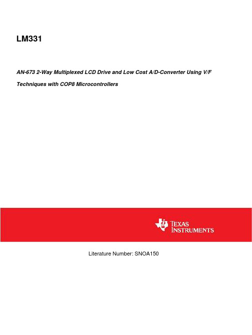
LM331为双列直插式8引脚芯片,其引脚框图如图1所示。
图1 LM331逻辑框图LM331 各引脚功能说明如下:脚 1 为脉冲电流输出端,内部相当于脉冲恒流源,脉冲宽度与内部单稳态电路相同;脚 2 为输出端脉冲电流幅度调节,RS 越小,输出电流越大;脚 3 为脉冲电压输出端,OC 门结构,输出脉冲宽度及相位同单稳态,不用时可悬空或接地;脚4 为地;脚 5 为单稳态外接定时时间常数RC ;脚6 为单稳态触发脉冲输入端,低于脚7 电压触发有效,要求输入负脉冲宽度小于单稳态输出脉冲宽度Tw ;脚7 为比较器基准电压,用于设置输入脉冲的有效触发电平高低;脚8 为电源Vcc , 正常工作电压范围为4~40V。
lm331详解

Versatile Monolithic V/Fs can Compute as Well as Convert with High AccuracyThe best of the monolithic voltage-to-frequency (V/F)con-verters have performance that’s so good it equals or ex-ceeds that of modular types.Some of these ICs can be designed into quite a variety of circuits because they’re notably versatile.Along with versatility and high performance come the advantages that are characteristic of all V/F con-verters,including good linearity,excellent resolution,wide dynamic range,and an output signal that’s easy to transmit as well as couple through an isolator.One of the recently introduced monolithic types,the LM131,has both high performance and a design that’s rather flex-ible.For instance,it can compute and convert at the same time;the computation is a part of the conversion.Among other functions,it can provide the product,ratio and square root of analog inputs.This IC has an internal reference for its conversion circuitry that’s also brought out to a pin,so it’s available to external circuits associated with the converter.Not surprisingly,it turns out that any deviations of the reference,due to process variations and temperature changes have equal and oppo-site effects on the scale factors of the converter and the external circuitry.(This presumes,of course,that the scale factor of the external circuitry is a linear function of voltage.)Precision Relaxation OscillatorBefore looking at some applications,quickly take a look at the basic circuit of an LM131V/F converter (Figure 1).Basically,this IC,like any V/F converter,is a precision relax-ation oscillator that generates a frequency linearly propor-tional to the input voltage.As might be expected,the circuit has a capacitor,C L ,with a sawtooth voltage on it.Generally speaking,the circuit is a feedback loop that keeps this capacitor charged to a voltage very slightly higher than the input voltage,V IN .If V IN is high,C L discharges relatively quickly through R L ,and the circuit generates a high fre-quency.If V IN is low,C L discharges slowly,and the converter puts out a low frequency.When C L discharges to a voltage equal to the input,the comparator triggers the one-shot.The one-shot closes the current switch and also turns on the output transistor.With the switch closed,current from the current source recharges C L to a voltage somewhat higher than the input.Charging continues for a period determined by R T and C T .At the end of this period,the one-shot returns to its quiescent state and C L resumes discharging.Resistor R S sets the amount of current put out by the current source.In fact,the current in pin 1,with the switch on,is identical to the current in pin 2.The latter pin is at a constant voltage (nominally 1.90V),so a given resistor value can set the operating currents.When connected to a high imped-ance buffer,this pin provides a stable reference for external circuits.The open-collector output at pin 3permits the output swing to be different from the converter’s supply voltage,if the load circuit requires.The supplies don’t have to be separate,however,and both the converter and its load can use the same voltage.National Semiconductor Application Note D August 1980Versatile Monolithic V/Fs Can Compute as Well as Convert with High AccuracyAN-D©2002National Semiconductor Corporation Precision Relaxation Oscillator(Continued)Steady as She GoesBy far the simplest of the circuits that make use of the reference output voltage from the LM131is one that simply ties this output pin right back to the signal input.This con-nection is just a V/F converter with a constant input,which makes it a constant-frequency oscillator.Even with thissimple circuit (Figure 2),variations in the reference voltage have two opposite effects that cancel each other out,so the circuit is particularly stable.In this type of circuit,the temperature-dependent internal delays tend to cancel as well,which isn’t true of relaxation oscillators based on op amps or comparators.00874201FIGURE 1.A voltage-to-frequency converter such as this is a relaxation oscillator with a frequency proportional tothe input voltage.Current pulses keep C L ’s average voltage slightly greater than the input voltage.A N -D 2Steady as She Goes(Continued)Resistors R L and R S are best taken from the same batch.(R L must be larger than R S,so it’s made up of two resistors.)By doing this,the tempco tracking,which is the criticalparameter,is five to ten times better than it would be if R Lwere a single30.1kΩresistor.Although the reference output,pin2,can’t be loaded withoutaffecting the converter’s sensitivity,the comparator input,pin7,has a high impedance so this connection does no harm.Frequency stability is typically±25ppm/˚C,even with anLM331,which as a V/F converter is specified only to150ppm/˚C maximum.From20Hz to20kHz,stability is excel-lent,and the circuit can generate frequencies up to120kHz.Although the simplest way of using the reference output is totie it back to the input,the reference can also be bufferedand amplified to supply such external circuitry as a resistivetransducer,which might be a strain gauge or a pot(Figure3).As in the stable oscillator already described,deviations ofthe internal reference voltage from the ideal cause the trans-ducer’s and the converter’s sensitivities to change equally inopposite directions,so the effects cancel.In this circuit,op amp A2buffers and amplifies the constantvoltage at pin2of the converter to provide the5V excitationfor the strain gauge.Amplifier A1,connected as an instru-mentation amplifier,raises the output of the strain gauge to ausable level while rejecting common-mode pickup.A potentiometer-type transducer works just as well with thiscircuit.Its wiper output takes the place of A1’s output asshown at the X.The reference terminal is both a constant voltage output anda current programming input.So far,it’s been shown simplywith one or two resistors going to ground.It is,however,afull-fledged signal input that accepts a signal from a currentsource quite well.3Steady as She Goes(Continued)This extra input is what enables the LM131to compute while converting.For instance,it will convert the ratio of two volt-ages to a frequency proportional to the ratio (Figure 4).The circuit is still a V/F converter,but has two signal inputs,both of them going to rather unorthodox places at that.The in-puts,shown as voltages,are converted to currents by two current pumps (voltage-to-current converters).Of course,if currents of the proper ranges are available,the current pumps aren’t needed.The left current pump,which includes Q1and A1,determines how fast capacitor C L discharges between output pulses.The other pump sets the current in the reference circuit to control the amount of recharge cur-rent when the one-shot fires.Tying the comparator input,pin 7,to the reference pin sets the comparator’s trip point at a constant voltage.To get an idea of how the circuit works,consider first the effect of,for instance,tripling the input voltage,V1.This make C L discharge to the comparator trip point three times as fast,so the frequency triples.Next,consider a givenchange,such as doubling the voltage at the other input,V2.This doubles the recharge current to C L during the fixed-width output pulse,which means C L ’s voltage in-creases twice as much during recharging.Since the dis-charge into Q1is linear (for V1constant),it takes twice as long for C L to discharge —the frequency becomes half of what it was before.Although the current pumps in Figure 4must have negative inputs,rearranging the op amps according to Figure 5makes them accept positive inputs instead.Trimming out the offset in the op amp gives the ratio converter better linearity and accuracy.The trim circuit in Figure 5a needs stable positive and negative supplies for the offset trimmer,while the one in Figure 5b needs only a stable positive supply.Unmarked components in Figure 5b are the same as in Figure 5a .Note that the full-scale range of the current pumps can be changed by varying the value of the input resistor(s).If either of these pump circuits is used with a single positive supply,00874205R1,R2,R3:Stable components with low tempco Q1:β≥330a00874206bFIGURE 5.These current pumps adapt the converter circuits in Figure 4and Figure 6to positive input voltages.Optional offset trimming improves linearity and accuracy,especially with input signals that have awide dynamic range.A N -D 4Steady as She Goes(Continued)the op amp should be a type such as 1/2LM358or 1/4LM324,which has a common-mode range that includes the negative-supply bus.Computing Square Roots ImplicitlyAn analog divider computes the square root of a signal when the signal is fed to the divider’s numerator input,and the output is fed back to the divider’s denominator input.00874207This type of computation is called implicit,because the end result of the computation is only implied,not explicitly stated by the equation that defines the computation.In the implicit square root computing loop described in the text,a V/F converter serves as a divider.Since it’s a con-verter,its inputs are voltages (or currents),but its output is a frequency.To connect its output back to one of its inputs so it will compute a square root means that its output frequency must be converted back to a voltage.This is taken care of by the frequency-to-voltage converter.It’ll Take ReciprocalsTaking the ratio of two inputs —in other words,doing division —is only one of the mathematical operations thatcan be combined with converting.Another one is a special case of division,which is taking reciprocals.In this instance,the numerator (V1in Figure 4)is held constant,and the denominator,V2,changes over a wide range such as one or two decades.In this case,since the frequency is the recip-rocal of the input,the period of the output is proportional to the input.When operated this way,the V2current pump should have an offset trimmer.A constant current circuit is still needed to discharge capacitor C L .Nonlinearity (that is,deviation from the ideal law)with an LM331is a little better than 1%for 10kHz full-scale.Increas-ing C T to 0.1µF reduces the nonlinearity to below 0.2%while decreasing full-scale output to 1kHz.Two inputs can also be multiplied while converting to a frequency.The multiplying converter circuit (Figure 6)that does this has a more elaborate current pump than the ratio circuit of Figure 4.This pump is really two cascaded circuits;it includes op amps A2and A3as well as transistors Q2and Q3.Current from this pump goes to pin 5to control the one-shot’s pulse width.(This current ranges from 13.3µA to 1.33µA.)As in the ratio circuit,the left current pump controls the discharge rate of C L .The other pump,however,controls the one-shot’s pulse width to vary the amount that C L charges during the pulse.If the V2input is close to zero,the current from the pump into pin 5is small,and the one-shot develops a wide pulse.This allows C L to charge quite a bit.It takes a relatively long time for C L to discharge to the comparator threshold,so the resulting frequency is low.As V2goes negative (a greater absolute magnitude),the output fre-quency rises.Op amp A3must have a common-mode range that extends to the positive supply voltage,which the speci-fied types do.Multiplying,dividing and converting can all be done at the same time by combining the V2input current pump of Figure 4with the circuit of Figure 6.If a scale-factor trimmer is needed,R4in Figure 6is a good choice,better than input resistors such as R1or ing the latter as trimmers would make the input impedance of the circuit change with trim setting.Two V/F converter ICs along with some extra circuitry will take the square root of a voltage input.Square root functions are used mostly to simulate natural laws,but also to linearize functions that have a natural square-law relationship.One of the latter is converting differential pressure to flow,where flow is proportional to the square root of differential pressure.AN-D5It’ll Take Reciprocals(Continued)Versatile Pin Functions Give Design FlexibilityTwo features —the reference and the one-shot —of the LM131/LM331V/F converter deserve a closer look because they are the key to its versatility.The simplified schematic of the chip,shown here along with a transducer and the com-ponents needed for a basic V/F converter,will help to illus-trate how these features work.The reference circuit,connected to pin 2,is both a constant voltage output and a current setting,scale-factor control input.The constant voltage can supply external circuitry,such as the transducer,that feeds the converter’s input.One great advantage of using the converter’s internal refer-ence to supply the external circuitry is that any variation in the reference voltage affects the sensitivities of the converter and the external circuitry by equal and opposite amounts,so the effects of the variation cancel.While providing a constant voltage output,pin 2also pro-vides scale-factor,or sensitivity control for the converter.Current supplied to an external circuit by this terminal comes from the supply (V S )through the current mirror and the transistor.The op amp drives this transistor to hold pin 2at a constant voltage equal to the internal reference,which is nominally 1.9V.The current mirror provides a current to the switch that’s essentially identical to that in pin 2.This means that a resistor to ground or a signal from a current source will set the current that is switched to pin 1.In most circuits,a capacitor goes from pin 1to ground,and the switched cur-rent from this pin recharges the capacitor during the pulse from the one-shot.The one-shot circuit is somewhat like the well known 555timer’s circuit.In the quiescent state,the reset transistor is on and holds pin 5near ground.When pin 7becomes more positive than pin 6(or pin 6falls below pin 7),the input comparator sets the flip-flop in the one-shot.The flip-flop turns on the current limited output transistor (pin 3)and switches the current coming from the current mirror to pin 1.The flip-flop also turns off the reset transistor,and the timing capacitor C T starts to charge toward V S .This charge is exponential,and C T ’s voltage reaches 2/3of V S in about00874209FIGURE 6.The product of two input voltages becomes an equivalent frequency in this converter.A current pump thatincludes op amps A2and A3controls the pulse duration of the converter’s internal one-shot.A N -D 6Versatile Pin Functions Give Design Flexibility(Continued)1.1R T C T time constants.(The quantity1.1is−ln0.333...) When pin5reaches this voltage,the one-shot’s comparator resets the flip-flop which turns off the current to pin1,dis-charges C T,and turns off the output transistor.If the voltages at pins6and7still call for setting the flip-flopafter pin5has reached2/3V S,internal logic not shown inthis simplified diagram overrides the reset signal from theone-shot’s own comparator,and the flip-flop stays set.In thisinstance,C T continues charging past2/3V S. 7Root Loop Computes(Continued)As a sign of this condition,when the converter hangs up,the one-shot’s timing node,pin 5,continues to charge well be-yond its normal peak of 2/3V S .As soon as the comparator A2detects this rise,it pulls up voltage V X ,current I 1in-creases,and the loop catches its breath again.After all these nonlinear computations,this last circuit is about as linear as it can be.It’s a precision,ultralinear V/F converter based on an LM331A (Figure 8)that has several detail refinements over previous V/F converter circuits.Choosing the proper components and trimming the tempco give less than 0.02%error and 0.003%nonlinearity for a ±20˚C range around room temperature.This circuit has an active integrator,which includes the op amp and the integrating feedback capacitor,C F .The integra-tor converts the input voltage,which is negative,into a positive-going ramp.When the ramp reaches the converter IC’s comparator threshold,the one-shot fires and switches a pulse of current to the integrator’s summing junction.This current makes the integrator’s output ramp down quickly.When the one-shot times out,the cycle repeats.00874211FIGURE 7.Two converter ICs generate an output frequency proportional to the square root of the input voltage.Thecircuit is an implicit loop in which IC1serves as a divider and V/F converter.This IC’s output goes back to itsdenominator input through F/V converter IC2to make the circuit output equal the input’s square root.A N -D 8Root Loop Computes(Continued)There are several reasons this converter circuit gives high performance:•A feedback limiter prevents the op amp from driving pin7 of the LM331A negative.The limiter circuit arrangement bypasses the leakage through CR5to ground via R5,so it won’t reach the summing junction.Bypassing leakage this way is especially important at high temperatures.•The offset trimming pot is connected to the stable1.9V reference at pin2instead of to a power supply bus that might be unstable and noisy.•A small fraction(180µV,full-scale)of the input voltage goes via R4to the R S network,which improves the non-linearity from0.004%to0.002%.•Resistors R2and R3are the same value,so that resis-tors such as Allen-Bradley type CC metal-film types can provide excellent tempco tracking at low cost.(This track-ing is very good when equal values come from the same batch.)Resistor R1should be a low tempco metal-film or wirewound type,with a maximum tempco of±10ppm/˚C or±25ppm/˚C.In addition,C T should be a polystyrene or Teflon type.Poly-styrene is rated to80˚C,while Teflon goes to150˚C.Both types can be obtained with a tempco of−110±30ppm/˚C. Choosing this tempco for C T makes the tempco,due to C T, of the full-scale output frequency110ppm/˚C.Using tight tolerance components results in a total tempco between0ppm/˚C and220ppm/˚C,so the tempco will never be negative.The voltage at CR1and R X has a tempco of −6mV/˚C,which can be used to compensate the tempco of the rest of the circuit.Trimming R X compensates for the tempco of the V/F IC,the capacitor,and all the resistors.A good starting value for selecting R X is430kΩ,which will give the135µA flowing out of pin2a slope of110ppm/˚C.If the output frequency increases with temperature,a little more conductance should be added in parallel with R X. When doing a second round of trimming,though,note that a resistor of,say, 4.3MΩ,has about the same effect on tempco when shunted across a220kΩresistor that it does when shunted across one of430kΩ,namely,−11ppm/˚C. This technique can give tempcos below±20ppm/˚C or even ±10ppm/˚C.00874212FIGURE8.An ultraprecision V/F converter,capable of better than0.02%error and0.003%nonlinearity for a±20˚C range about room temperature,augments the basic converter with an external integrator.AN-D9Root Loop Computes(Continued)Some precautions help this procedure converge:1.Use a good capacitor for C T .The cheapest polystyrene capacitors will shift in value by 0.05%or more per tem-perature cycle.The actual temperature sensitivity would be indistinguishable from the hysteresis,and the circuit would never be stable.2.After soldering,bake and/or temperature-cycle the cir-cuit (at a temperature not exceeding 75˚C if C T is poly-styrene)for a few hours,to stabilize all components and to relieve the strains from soldering.3.Don’t rush the trimming.Recheck the room temperaturevalue,before and after the high temperature data aretaken,to ensure that hysteresis per cycle is reasonably low.4.Don’t expect a perfect tempco at −25˚C if the circuit istrimmed for ±5ppm/˚C between 25˚C and 60˚C.If it’s been trimmed for zero tempco while warm,none of its components will be linear to much better than 5ppm/˚C or 10ppm/˚C when it’s cold.The values shown in this circuit are generally optimum for ±12V to ±16V regulated supplies but any stable supplies between ±4V and ±22V would be usable,after changing a few component values.LIFE SUPPORT POLICYNATIONAL’S PRODUCTS ARE NOT AUTHORIZED FOR USE AS CRITICAL COMPONENTS IN LIFE SUPPORT DEVICES OR SYSTEMS WITHOUT THE EXPRESS WRITTEN APPROVAL OF THE PRESIDENT AND GENERAL COUNSEL OF NATIONAL SEMICONDUCTOR CORPORATION.As used herein:1.Life support devices or systems are devices or systems which,(a)are intended for surgical implant into the body,or (b)support or sustain life,and whose failure to perform when properly used in accordance with instructions for use provided in the labeling,can be reasonably expected to result in a significant injury to the user.2.A critical component is any component of a life support device or system whose failure to perform can be reasonably expected to cause the failure of the life support device or system,or to affect its safety or effectiveness.National Semiconductor Corporation AmericasEmail:support@National Semiconductor EuropeFax:+49(0)180-5308586Email:europe.support@Deutsch Tel:+49(0)6995086208English Tel:+44(0)8702402171Français Tel:+33(0)141918790National Semiconductor Asia Pacific Customer Response Group Tel:65-2544466Fax:65-2504466Email:ap.support@National Semiconductor Japan Ltd.Tel:81-3-5639-7560Fax:81-3-5639-7507A N -DV e r s a t i l e M o n o l i t h i c V /F s C a n C o m p u t e a s W e l l a s C o n v e r t w i t h H i g h A c c u r a c yNational does not assume any responsibility for use of any circuitry described,no circuit patent licenses are implied and National reserves the right at any time without notice to change said circuitry and specifications.。
ELM331中文资料(ELM Electronics)中文数据手册「EasyDatasheet - 矽搜」

逻辑电路.正在进行脚测量可以
然后,可以使用任一中断,或作为一个忙标志
在这新结果能时钟下降沿...
备用电池是另一种选择可能是
加入到这个电路,但后来考虑应该是 给使用ELM341低功率恒温器...
+12V
0.1µF
78L05
RTEMP 10KΩ @25°C
0.1µF
1
2 见文
3
4
RSET 18KΩ
8 7 6 5
10KΩ
0.1µF
1N400电器
到 加热 控制
2N3904
560Ω LED
图1.备份加热控制温控器
8 VSS 7 Out 6 MIP 5 Cap
框图 R1
reset 4
2 3
R2
5
VDD
控制
看家狗
Timer
测量过程中(繁忙)
超量程
模拟到 数位 变流器
R1 R 2 3连续
测量
6 MIP 7 Out
芯片中文手册,看全文,戳
引脚说明
VDD (引脚1) 该引脚为正电源引脚,应始终在电路中最产品极 一点.
300 mil Plastic DIP............................... ELM331P
200 mil SOIC..................................... ELM331SM
芯片中文手册,看全文,戳
ELM331
绝对最大额定值
复位(引脚4)
该低电平有效复位输入.内部上拉
电阻提供方便.如果未使用,
该管脚可被连接到V
DD 或悬空.
ELM331
盖(引脚5)
温度测量是通过确定充电和放电该产
LM331中文资料_中文手册_芯片中文资料_芯片中文手册
LM331中文资料_中文手册_芯片中文资料_芯片中文手册电压-频率变换器LM331LM331是美国NS公司生产的性能价格比较高的集成芯片。
LM331可用作精密的频率电压(F/V)转换器、A/D转换器、线性频率调制解调、长时间积分器以及其他相关的器件。
LM331为双列直插式8脚芯片,其引脚如图3所示。
LM331内部有(1)输入比较电路、(2)定时比较电路、(3)R-S触发电路、(4)复零晶体管、(5)输出驱动管、(6)能隙基准电路、(7)精密电流源电路、(8)电流开关、(9)输出保护点路等部分。
输出管采用集电极开路形式,因此可以通过选择逻辑电流和外接电阻,灵活改变输出脉冲的逻辑电平,从而适应TTL、DTL和CMOS等不同的逻辑电路。
此外,LM331可采用单/双电源供电,电压范围为4,40V,输出也高达40V。
引脚1(PIN1)为电流源输出端,在f(PIN3)输出逻辑低电平时,电流源,输出对电容,充电。
,,,引脚2(PIN2)为增益调整,改变,的值可调节电路转换增益的大小。
,引脚3(PIN3)为频率输出端,为逻辑低电平,脉冲宽度由,和,决定。
tt引脚4(PIN4)为电源地。
引脚5(PIN5)为定时比较器正相输入端。
引脚6(PIN6)为输入比较器反相输入端。
引脚7(PIN7)为输入比较器正相输入端。
引脚8(PIN8)为电源正端。
LM331频率电压转换器V/F变换和F/V变换采用集成块LM331,LM331是美国NS公司生产的性能价格比较高的集成芯片,可用作精密频率电压转换器用。
LM331采用了新的温度补偿能隙基准电路,在整个工作温度范围内和低到4.0V电源电压下都有极高的精度。
同时它动态范围宽,可达100dB;线性度好,最大非线性失真小于0.01,,工作频率低到0.1Hz时尚有较好的线性;变换精度高,数字分辨率可达12位;外接电路简单,只需接入几个外部元件就可方便构成V/F或F/V等变换电路,并且容易保证转换精度。
LM331在AD转换电路中的应用
LM331在AD转换电路中的应用摘要:本文主要介绍一种应用V/F转换器LM331实现A/D转换的电路,本电路价格低廉,外围电路简单, 适合应用在转换速度不太高的场合应用.本文包括硬件电路和软件程序的实现.关键词:A/D转换器,V/F转换器, 高精度.引言: 数据的采集与处理广泛地应用在自动化领域中,由于应用的场合不同,对数据采集与处理所要求的硬件也不相同.在控制过程中,有时要对几个模拟信号进行采集与处理,这些信号的采集与处理对速度要求不太高,一般采用AD574或ADC0809等芯片组成的A/D转换电路来实现信号的采集与模数转换,而AD574和ADC0809等A/D转换器价格较贵,线路复杂,从而提高了产品价格和项目的费用.在本文中,从实际应用出发,给出了一种应用V/F转换器LM331芯片组成的A/D转换电路,V/F转换器LM331芯片能够把电压信号转换为频率信号,而且线性度好,通过计算机处理,再把频率信号转换为数字信号,就完成了A/D转换。
它与AD574等电路相比,具有接线简单,价格低廉,转换精度高等特点,而且LM331芯片在转换过程中不需要软件程序驱动,这与AD574等需要软件程序控制的A/D转换电路相比,使用起来方便了许多。
一. 芯片简介LM331是美国NS公司生产的性能价格比比较高的集成芯片。
它是当前最简单的一种高精度V/F转换器、A/D转换器、线性频率调制解调、长时间积分器以及其它相关的器件。
LM331为双列直插式8引脚芯片,其引脚框图如图1所示。
图1 LM331逻辑框图LM331各引脚功能说明如下:脚1 为脉冲电流输出端,内部相当于脉冲恒流源,脉冲宽度与内部单稳态电路相同;脚2 为输出端脉冲电流幅度调节,RS 越小,输出电流越大;脚3 为脉冲电压输出端,OC 门结构,输出脉冲宽度及相位同单稳态,不用时可悬空或接地;脚4 为地;脚5 为单稳态外接定时时间常数RC ;脚6 为单稳态触发脉冲输入端,低于脚7 电压触发有效,要求输入负脉冲宽度小于单稳态输出脉冲宽度Tw ;脚7 为比较器基准电压,用于设置输入脉冲的有效触发电平高低;脚8 为电源Vcc , 正常工作电压范围为4~40V。
LM3108G 高压电网智能保护模块使用说明书
331中文操作安装手册
MODEL331型H2S分析仪操作和安装手册目录1介绍--------------------------------------------------------------------3 2说明--------------------------------------------------------------------3 3操作原理----------------------------------------------------------------3 4安装和启动--------------------------------------------------------------5 4.1选择取样点------------------------------------------------------------5 4.2取样的量和流速--------------------------------------------------------5 4.3样气状态--------------------------------------------------------------5 4.3.2稀释面板------------------------------------------------------------7 4.3.3测量总硫选项--------------------------------------------------------8 4.3.4测总硫的预检和启动--------------------------------------------------8 4.4安装程序-------------------------------------------------------------11 4.5喷射口的安装---------------------------------------------------------12 5操作界面---------------------------------------------------------------13 6标定和报警-------------------------------------------------------------14 7纸带更换---------------------------------------------------------------15 8用户连接---------------------------------------------------------------16 9维护和故障处理---------------------------------------------------------18 10推荐的备件清单--------------------------------------------------------19 11可选择电脑图形界面GUI------------------------------------------------20 12图片------------------------------------------------------------------25 13转换因素--------------------------------------------------------------27 14工厂标定数据----------------------------------------------------------27 15系统图----------------------------------------------------------------27图表目录图1:样气流动示意图------------------------------------------------------4图2:取样室和部件--------------------------------------------------------4图3:传感器模块和芯片----------------------------------------------------5图4:典型的隔膜取样系统,c/w自动螺线管标定------------------------------6图5:典型的带过滤的取样系统---------------------------------------------6图6:纸带盘的背面图-----------------------------------------------------7图7:稀释的取样系统,在16"*24"的面板上---------------------------------7图8:Model331总硫分析仪和流程示意图------------------------------------8图9:反应炉的泄漏检查----------------------------------------------------9图10:更换反应管--------------------------------------------------------10图11:喷射器连接--------------------------------------------------------13图13:纸带更换程序------------------------------------------------------16图14:旁路和菜单---------------------------------------------------------14图15:卷轴按钮-----------------------------------------------------------14图16:控制电路板---------------------------------------------------------17图17:4-20mA电源选择-----------------------------------------------------17图19:继电器输出原理图---------------------------------------------------18表1:备件----------------------------------------------------------------19图20:通讯线缆-----------------------------------------------------------20图21:主板---------------------------------------------------------------25图22:显示板-------------------------------------------------------------26图23:传感器输入板-------------------------------------------------------26图24:纸带内部台板-------------------------------------------------------27表2:H2S测量时常用的单位换算---------------------------------------------271.介绍331型H2S分析仪通过软件和硬件的配置,能够测量气体和液体中的宽范围高浓度的H2S 含量。
- 1、下载文档前请自行甄别文档内容的完整性,平台不提供额外的编辑、内容补充、找答案等附加服务。
- 2、"仅部分预览"的文档,不可在线预览部分如存在完整性等问题,可反馈申请退款(可完整预览的文档不适用该条件!)。
- 3、如文档侵犯您的权益,请联系客服反馈,我们会尽快为您处理(人工客服工作时间:9:00-18:30)。
电压-频率变换器LM331LM331是美国NS公司生产的性能价格比较高的集成芯片。
LM331可用作精密的频率电压(F/V)转换器、A/D转换器、线性频率调制解调、长时间积分器以及其他相关的器件。
LM331为双列直插式8脚芯片,其引脚如图3所示。
LM331内部有(1)输入比较电路、(2)定时比较电路、(3)R-S触发电路、(4)复零晶体管、(5)输出驱动管、(6)能隙基准电路、(7)精密电流源电路、(8)电流开关、(9)输出保护点路等部分。
输出管采用集电极开路形式,因此可以通过选择逻辑电流和外接电阻,灵活改变输出脉冲的逻辑电平,从而适应TTL、DTL和CMOS 等不同的逻辑电路。
此外,LM331可采用单/双电源供电,电压范围为4~40V,输出也高达40V。
引脚1(PIN1)为电流源输出端,在f0(PIN3)输出逻辑低电平时,电流源IR输出对电容CL充电。
引脚2(PIN2)为增益调整,改变RS的值可调节电路转换增益的大小。
引脚3(PIN3)为频率输出端,为逻辑低电平,脉冲宽度由Rt和Ct决定。
引脚4(PIN4)为电源地。
引脚5(PIN5)为定时比较器正相输入端。
引脚6(PIN6)为输入比较器反相输入端。
引脚7(PIN7)为输入比较器正相输入端。
引脚8(PIN8)为电源正端。
LM331频率电压转换器V/F变换和F/V变换采用集成块LM331,LM331是美国NS公司生产的性能价格比较高的集成芯片,可用作精密频率电压转换器用。
LM331采用了新的温度补偿能隙基准电路,在整个工作温度范围内和低到4.0V电源电压下都有极高的精度。
同时它动态范围宽,可达100dB;线性度好,最大非线性失真小于0.01%,工作频率低到0.1Hz时尚有较好的线性;变换精度高,数字分辨率可达12位;外接电路简单,只需接入几个外部元件就可方便构成V/F或F/V等变换电路,并且容易保证转换精度。
图2是由LM331组成的电压频率变换电路,LM331内部由输入比较器、定时比较器、R-S触发器、输出驱动、复零晶体管、能隙基准电路和电流开关等部分组成。
输出驱动管采用集电极开路形式,因而可以通过选择逻辑电流和外接电阻,灵活改变输出脉冲的逻辑电平,以适配TTL、DTL和CMOS等不同的逻辑电路。
当输入端Vi+输入一正电压时,输入比较器输出高电平,使R-S触发器置位,输出高电平,输出驱动管导通,输出端f0为逻辑低电平,同时电源Vcc也通过电阻R2对电容C2充电。
当电容C2两端充电电压大于Vcc的2/3时,定时比较器输出一高电平,使R-S触发器复位,输出低电平,输出驱动管截止,输出端f0为逻辑高电平,同时,复零晶体管导通,电容C2通过复零晶体管迅速放电;电子开关使电容C3对电阻R3放电。
当电容C3放电电压等于输入电压Vi时,输入比较器再次输出高电平,使R-S触发器置位,如此反复循环,构成自激振荡。
输出脉冲频率f0与输入电压Vi成正比,从而实现了电压-频率变换。
其输入电压和输出频率的关系为:fo=(Vin×R4)/(2.09×R3×R2×C2)由式知电阻R2、R3、R4、和C2直接影响转换结果f0,因此对元件的精度要有一定的要求,可根据转换精度适当选择。
电阻R1和电容C1组成低通滤波器,可减少输入电压中的干扰脉冲,有利于提高转换精度。
同样,由LM331也可构成频率-电压转换电路。
LM331压频变换器的原理及应用摘要:介绍了集成电路LM331的结构和特点,分析了V/F和F/V电路的工作原理。
同时也给出了一些应用的例子。
关键词:电压-频率变换;频率-电压变换;LM3311. 概述LM331是美国NS公司生产的性能价格比较高的集成芯片,可用作精密频率电压转换器、A/D转换器、线性频率调制解调、长时间积分器及其他相关器件。
LM331采用了新的温度补偿能隙基准电路,在整个工作温度范围内和低到4.0V电源电压下都有极高的精度。
LM331的动态范围宽,可达100dB;线性度好,最大非线性失真小于0.01%,工作频率低到0.1Hz时尚有较好的线性;变换精度高,数字分辨率可达12位;外接电路简单,只需接入几个外部元件就可方便构成V/F或F/V等变换电路,并且容易保证转换精度。
LM331的内部电路组成如图1所示。
由输入比较器、定时比较器、R-S触发器、输出驱动管、复零晶体管、能隙基准电路、精密电流源电路、电流开关、输出保护管等部分组成。
输出驱动管采用集电极开路形式,因而可以通过选择逻辑电流和外接电阻,灵活改变输出脉冲的逻辑电平,以适配TTL、DTL和CMOS等不同的逻辑电路。
LM331可采用双电源或单电源供电,可工作在4.0~40V之间,输出可高达40V,而且可以防止Vcc短路。
2. 工作原理2.1 电压—频率变换器图2是由LM331组成的电压椘德时浠坏缏贰M饨拥缱鑂t、C t和定时比较器、复零晶体管、R-S触发器等构成单稳定时电路。
当输入端Vi+输入一正电压时,输入比较器输出高电平,使R-S触发器置位,Q输出高电平,输出驱动管导通,输出端f0为逻辑低电平,同时,电流开关打向右边,电流源I R对电容C L充电。
此时由于复零晶体管截止,电源Vcc也通过电阻R t对电容C t充电。
当电容C t两端充电电压大于Vcc的2/3时,定时比较器输出一高电平,使R-S触发器复位,Q输出低电平,输出驱动管截止,输出端f0为逻辑高电平,同时,复零晶体管导通,电容C t通过复零晶体管迅速放电;电流开关打向左边,电容C l对电阻R L放电。
当电容C L放电电压等于输入电压Vi时,输入比较器再次输出高电平,使R-S触发器置位,如此反复循环,构成自激振荡。
图3画出了电容C t、C l充放电和输出脉冲f0的波形。
设电容C L的充电时间为t1,放电时间为t2,则根据电容C L上电荷平衡的原理,我们有:(I R-V L/R L)t1=t2V L/R L从上式可得:f0=1/(t1+t2)=V L/(R L I R t1)实际上,该电路的VL在很少的范围内(大约10mV)波动,因此,可认为V L=V t,故上式可以表示为:f0==V t/(R L I R t1)可见,输出脉冲频率f0与输入电压V i成正比,从而实现了电压-频率变换。
式中I R由内部基准电压源供给的1.90V 参考电压和外接电阻R s决定,I R=1.90/Rs,改变R s的值,可调节电路的转换增益,t1由定时元件R t和C t决定,其关系是t1=1.1R t C t,典型值R t=6.8kΩ,C t=0.01μF,t1=7.5μs。
由f0=V i/(R L I R t)可知,电阻R s、R l、R t和电容C t直接影响转换结果f0,因此对元件的精度要有一定的要求,可根据转换精度适当选择。
电容C l对转换结果虽然没有直接的影响。
但应选择漏电流小的电容器。
电阻R1和电容C1组成低通滤波器,可减少输入电压中的干扰脉冲,有利于提高转换精度。
2.2 频率-电压变换器由LM331构成的频率-电压转换电路如图4所示,输入脉冲f i经R1、C1组成的微分电路加到输入比较器的反相输入端。
输入比较器的同相输入端经电阻R2、R3分压而加有约2Vcc/3的直流电压,反相输入端经电阻R1加有Vcc的直流电压。
当输入脉冲的下降沿到来时,经微分电路R1、C1产生一负尖脉冲叠加到反相输入端的Vcc上,当负向尖脉冲大于Vcc/3时,输入比较器输出高电平使触发器置位,此时电流开关打向右边,电流源I R对电容C L充电,同时因复零晶体管截止而使电源Vcc通过电阻R t对电容C t充电。
当电容C L两端电压达到2Vcc/3时,定时比较器输出高电平使触发器复位,此时电流开关打向左边,电容C L通过电阻R L放电,同时,复零晶体管导通,定时电容C t迅速放电,完成一次充放电过程。
此后,每当输入脉冲的下降沿到来时,电路重复上述的工作过程。
从前面的分析可知,电容C L的充电时间由定时电路R t、C t决定,充电电流的大小由电流源IR决定,输入脉冲的频率越高,电容C L上积累的电荷就越多输出电压(电容C L两端的电压)就越高,实现了频率-电压的变换。
按照前面推导V/F表达式的方法,可得到输出电压V O与f i的关系为:V O=2.09R l R t C t f i/R s电容C1的选择不宜太小,要保证输入脉冲经微分后有足够的幅度来触发输入比较器,但电容C1小些有利于提高转换电路的抗干扰能力。
电阻R L和电容C L组成低通滤波器。
电容C L大些,输出电压V O的纹波会小些,电容C L小些,当输入脉冲频率变化时,输出响应会快些。
这些因素在实际运用时要综合考虑。
3. 应用图5为由两块LM331组成的遥测电路。
在人员不能进入或不易进入的场合,通过传感器将被测量转换为电压,经运算放大器放大为0~10V电压信号,由LM331进行V/F变换为脉冲信号,通过长双绞线传输到测量室,在测量室内通过光电耦合器转换为幅度稳定的脉冲电压,此脉冲电压再经LM331进行F/V变换为电压进行测量,从而可避免直接导线连接到测量室而造成的线路衰减或干扰,提高测量精度。
当前,12位以上的A/D转换器的价格仍较昂贵,用V/F变换器来代替A/D转换器,在要求速度不太高的场合是一种较好的选择。
用LM331构成的A/D变换器采集系统接口电路如图6所示。
从传感器来的毫伏级的电压信号经低温漂运算放大器INA101放大到0~10V后加到V/F变换器LM331的输入端,从频率输出端f0输出的频率信号加到单片机8031的输入端T1上。
根据分辨率的要求利用软件(限于篇幅,程序部分略)处理,最后得到A/D转换的结果。