Module工艺流程介绍
芯片模块工艺流程9个步骤

芯片模块工艺流程9个步骤英文回答:The process of chip module fabrication involves several steps. Here, I will outline the nine main steps involved in the process.1. Substrate Preparation: The first step is to prepare the substrate on which the chip will be built. Thisinvolves cleaning the substrate and depositing a thin layer of material, such as silicon dioxide, to provide insulation.2. Deposition: In this step, various layers ofmaterials are deposited onto the substrate. This can bedone using techniques like physical vapor deposition (PVD)or chemical vapor deposition (CVD). For example, a layer of metal may be deposited to serve as the conductive pathwaysin the chip.3. Photolithography: Photolithography is a key step inchip fabrication. A photosensitive material called a photoresist is applied to the substrate, and a pattern is created using a mask. The pattern is then transferred to the photoresist using ultraviolet light. This step defines the features and structures of the chip.4. Etching: Etching is used to remove unwanted materials from the substrate. This can be done through wet etching or dry etching processes. For example, if a layer of metal needs to be removed to create a specific pattern, a chemical etchant may be used.5. Ion Implantation: Ion implantation is used to introduce dopants into the substrate to modify its electrical properties. This step helps create the desired characteristics of the chip, such as creating regions of different conductivity.6. Annealing: After ion implantation, annealing is performed to activate the dopants and repair any damage caused during the implantation process. This involves heating the substrate to high temperatures for a specificduration.7. Metallization: Metallization involves depositing a layer of metal onto the chip to create interconnects between different components. This step is crucial for ensuring proper electrical connectivity within the chip.8. Testing: Once the chip is fabricated, it undergoes extensive testing to ensure its functionality and performance. This includes electrical testing, functional testing, and reliability testing. Any defects or issues are identified and addressed during this stage.9. Packaging: The final step is packaging the chip. This involves encapsulating the chip in a protective casing and connecting it to external leads or pins. The packaged chip is then ready for use in various electronic devices.中文回答:芯片模块的制造过程涉及几个步骤。
Module工艺流程介绍(DOC)
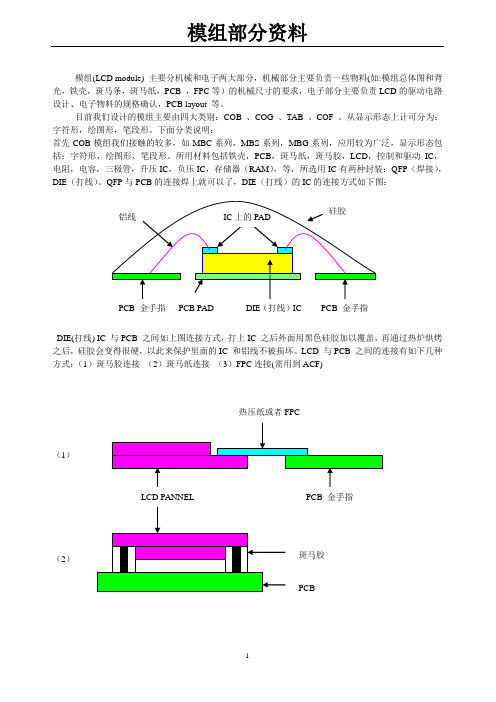
模组(LCD module) 主要分机械和电子两大部分,机械部分主要负责一些物料(如:模组总体图和背光,铁壳,斑马条,斑马纸,PCB ,FPC 等)的机械尺寸的要求,电子部分主要负责LCD 的驱动电路设计、电子物料的规格确认,PCB layout 等。
目前我们设计的模组主要由四大类别:COB 、COG 、TAB 、COF 。
从显示形态上计可分为:字符形,绘图形,笔段形。
下面分类说明:首先COB 模组我们接触的较多,如MBC 系列,MBS 系列,MBG 系列,应用较为广泛,显示形态包括:字符形,绘图形,笔段形。
所用材料包括铁壳,PCB ,斑马纸,斑马胶,LCD ,控制和驱动IC ,电阻,电容,三极管,升压IC ,负压IC ,存储器(RAM ),等,所选用IC 有两种封装:QFP (焊接),DIE (打线)。
QFP 与PCB 的连接焊上就可以了,DIE (打线)的IC 的连接方式如下图:DIE(打线) IC 与PCB 之间如上图连接方式,打上IC 之后外面用黑色硅胶加以覆盖,再通过热炉烘烤之后,硅胶会变得很硬,以此来保护里面的IC 和铝线不被损坏。
LCD 与PCB 之间的连接有如下几种方式:(1)斑马胶连接 (2)斑马纸连接 (3)FPC 连接(需用到ACF)(1)(2)在驱动方面,我们可以参照如下框图:以16*1 character 为例:KS0066(即S6A0069)为字符形模组LCD控制和驱动IC,它包括:16 Common 和40 Segment signal 输出,可以驱动8*2或16*1字符形模组,它有两种封装(80QFP and 80 DIE), 常与S6A0065(KS0065)或S6A2067(KS0063A)配合使用来驱动更多字符的LCD,我们最常用的字符形模组的控制IC :KS0066(S6A0069)和KS0070(S6A0070),驱动器:KS0065(S6A0065)和KS0063(S6A2067),KS0066上面有说过能单独驱动16*1字符或8*2字符,KS0070有16 COM 和80 SEG 输出,能单独驱动16*2字符;KS0065 、KS0063是只含驱动器,不含控制器,KS0065有40 channel 输出,KS0063 有80 channel 输出。
TFT-LCDARRAY,CELL,MODULE工艺技术介绍

时间/min
1000 800 600 400 200 0
1.节省时间:1462-1398=64min
2.节省设备:1套 InlinePR+曝光机
6
二、4Mask与5Mask工艺对比
5 Mask – D工程和I 工程
曝光
4 Mask – D/I 工程
曝光 DI-工艺
I-工艺
D1-WE
I-DE 曝光 D-工艺
SOURCE
电路部件 偏光板
P-SiNx
DRAIN
n+ a-Si
GLASS a-Si GATE
G-SiNx
3
一、 TFT的基本构造
接触孔 ITO像素电极 PI工程
C工程
SOURCE DRAIN D工程 P-SiNx
n+ a-Si a-Si I 工程 GATE
GLASS
G-SiNx
G工程
4
二、4Mask与5Mask工艺对比
干刻(DE)
刻蚀掉未被光刻胶掩蔽的金属膜
刻蚀掉未被光刻胶掩蔽的非金属膜
剥离
去掉残余的光刻胶8 Nhomakorabea洗净
卸料
周转盒
MS
传送装置 机械手 气刀
高压喷射
刷洗 药液喷淋 UV 传送装置
机械手
装料 9
洗净
UV 药液 刷子 高圧 MS A/K
P U V
D A
排 水
P 刷洗
P 高 压 喷射
纯 水
排 水 M S
D A
药 液
洗净 功能
洗净对象 作 用
氧化分解 有机物 (浸润性改善) UV/O3
溶 解 有机物 溶 解
机械剥离 微粒子 (大径)
模块工艺流程9个步骤
模块工艺流程9个步骤英文回答:Module process consists of 9 steps. Let me explain each step in detail.Step 1: Planning and Design.In this step, we plan and design the module process. We determine the objectives, requirements, and specifications of the module. For example, if we are designing a modulefor a car, we would determine the size, shape, and functionality of the module.Step 2: Material Selection.In this step, we select the materials that will be used in the module. We consider factors such as strength, durability, and cost. For example, if we are designing a module for a smartphone, we would select materials that arelightweight, strong, and cost-effective.Step 3: Cutting and Shaping.In this step, we cut and shape the materials according to the design specifications. We use tools such as saws, drills, and milling machines. For example, if we are designing a module for a furniture piece, we would cut the wood into the desired shapes and sizes.Step 4: Assembly.In this step, we assemble the different components of the module. We use techniques such as welding, soldering, and gluing. For example, if we are designing a module for a computer, we would assemble the motherboard, processor, and other components.Step 5: Testing and Quality Control.In this step, we test the module to ensure that it meets the required standards and specifications. We checkfor any defects or malfunctions. For example, if we are designing a module for a refrigerator, we would test it for temperature control, energy efficiency, and noise level.Step 6: Finishing.In this step, we apply finishing touches to the module. We may paint, polish, or coat the module to enhance its appearance and protect it from damage. For example, if we are designing a module for a car, we would apply a coat of paint to give it a glossy finish.Step 7: Packaging.In this step, we package the module for transportation and storage. We use materials such as boxes, bubble wrap, and pallets. For example, if we are designing a module for a television, we would package it in a box with foam padding to protect it during shipping.Step 8: Distribution.In this step, we distribute the modules to the intended markets or customers. We may use various distribution channels such as wholesalers, retailers, or online platforms. For example, if we are designing a module for a smartphone, we would distribute it to mobile phone stores or sell it online.Step 9: Maintenance and Support.In this step, we provide maintenance and support services to the customers who have purchased the module. We may offer warranties, repairs, or technical assistance. For example, if a customer faces any issues with a module for a washing machine, we would provide them with repair services or guide them through troubleshooting.中文回答:模块工艺流程包括9个步骤。
载波通信模块生产工艺流程
载波通信模块生产工艺流程英文回答:Carrier Communication Module Production Process Flow.The production process flow for carrier communication modules involves several key steps to ensure the quality and functionality of the final product. Here is a general overview of the process:1. Raw Material Inspection: The process begins with the inspection of raw materials, such as printed circuit boards (PCBs), components, and connectors, to ensure that they meet the required specifications.2. PCB Assembly: The PCBs are assembled with the necessary electronic components, including resistors, capacitors, and transistors. Automated surface mount technology (SMT) machines and solder reflow ovens are used to place and solder the components onto the PCBs.3. Functional Testing: The assembled PCBs undergo functional testing to verify their electrical functionality and performance. This includes testing for signal integrity, power consumption, and adherence to design specifications.4. Component Assembly: The tested PCBs are assembledwith additional components, such as heat sinks, connectors, and enclosures. These components provide mechanical support, environmental protection, and interface with other devices.5. Software Integration: The firmware and software required for the module's operation are integrated and installed. This includes programming microcontrollers and configuring software parameters to meet the specific requirements of the application.6. System Integration: The module is integrated with other components, such as antennas and power supplies, to form a complete communication system. This step involves testing the overall system functionality and performance.7. Environmental Testing: The completed module undergoes environmental testing to ensure that it can withstand the expected operating conditions. This includes testing for temperature extremes, humidity, vibration, and shock.8. Quality Control: Throughout the production process, rigorous quality control measures are implemented to ensure the reliability and performance of the final product. This includes inspection, testing, and documentation.9. Packaging and Shipping: The finished carrier communication modules are packaged and shipped to customers for use in various applications, such as telecommunications, networking, and industrial automation.中文回答:载波通信模块生产工艺流程。
模组工艺培训 PPT

ACF来料为卷盘式包装,使 用时如右图所示安装在机 器相应位置。
ACF安装路径
MODULE工艺流程介绍——COG邦定(贴ACF) 机器按照已设定长度,将ACF剪切后粘贴在LCD上。 剪切方式为半切,过深或过浅都会造成ACF贴附问题。
Base film
ACF CUTTER
ACF贴合后由机器按设置的参数自动检查贴附位置;要求 表面平整无气泡、褶皱;形状规则(无缺角、卷边)。
MODULE工艺流程介绍——FPC邦定
温度、压力、时间是ACF贴合和FPC邦定的重要参数。 一般情况下,ACF贴合:80±10℃、1MPa、1s
气
缺
泡
角
MODULE工艺流程介绍——COG邦定(预邦) 预邦是COG邦定机的核心,包括IC供料和预邦定两部分。
将IC安放在托盘架上
将托盘架安放 在托盘箱里
将托盘箱在机器里设置好, 并保证无倾斜;由机器将IC 传送至预邦压头下
MODULE工艺流程介绍——COG邦定(预邦)
预邦定的作用是将IC Bump与LCD引脚精确对位,并粘接IC。 邦定机利用CCD识别IC及玻璃mark,计算相对坐标后进行精确 对位。(邦定机对位精度可以达到±3um) 一般情况下,机器预邦参数:70±10℃、10~15N、0.5s
COG:中小尺寸产品IC封装的主流技术。 使用ACF将裸片IC直接连接在LCD上。 制程简化、Pitch小、成本低,只是返 修稍困难。
MODULE结构介绍——COG模块
利用COG方式封装驱动IC的液晶显示模块称为COG模块。 COG模块的基本结构如下图所示:
MODULE工艺流程介绍
大家应该也有点累了,稍作休息
Tray 上料
单片上料
LCD loading有两种结构,可利用Tray盘上料(适合较小尺寸), 也可人工单片放在机器传送带上(大尺寸)。单片放置时须注 意间隔不要太密,避免造成LCD电极划伤。
Module工艺流程基础培训
1. Auto Clave : 作用是去除POL和Panel之间的气泡,并增加Pol的粘稠力,大致分 为三步:① Loading Unit ② Auto Clave ③ Unloading Unit
• COF : Chip On Film 薄膜芯片集成
• OLB : Outer Lead Bonding 外引线绑定
• S/C : Shield Cover 屏蔽板
• B/L : Back Light 背光源
• B/Z : Bezel 边框
• R/W : Rework 返工
• RMA : Return Material Authorization
Cullet Remove
CELL 贴附 ROLLER
POL
STAGE
BRUSH 回转方向
CELL 进行方向
BRUSH
Cell Cleaner
搬送ROLL
Cell 进行方向
倾斜上升
Pol Attacher
旋转贴附
作用 材料
将Polarizer贴附到Cell上下表面的工程 Polarizer -TFT、CF
2.1 Module工艺构成
MDC
M
前工程
O
D
U
L
E
后工程
R/W
LOT ASSIGN POL OLB
ASS’Y
LINE IN ASS’Y INSPECTION
AGING TEST FINEL INSPECTION
APP INSPECTION PACKING
2.2 Module工艺流程
Cleaning Auto Clave
Cullet Cleaner是用刀片在cell表面进行旋转,同时水 平方向喷洒DIW,以清除Cell表面碎玻璃或异物。
Module-初级-Module工艺流程-20160415【宋立辉】-程巍-宋艳辉
1.Yield 2.CAPA-设备稼动率, Tact Time
3.1 OLB-PCB工艺
PCB Buffer
X PCB Bonding
Y PCB Bonding
Silicone dispensing
PCB Inspection
作 材
用 料
将TCP Lead 与 PCB Lead 通过ACF连接,对应电路导通 PCBA ACF Silicone resin
5.最终清洗
6.A/K(风刀)吹干
2.POL工艺
各流程知识集锦
POL Cleaner:毛刷清洗部、研磨部(研磨带&去离子水)、干燥部
POL Attach :贴附CF侧& TFT侧偏光片 CF侧POL保护膜上Mark颜色为红色,TFT侧的为蓝色 CF侧 POL TFT侧 POL
Auto Clave:通过时间、压力、温度条件下进行脱泡增加黏着力
3.2 OLB-FOB工艺
FOB工序模拟图:
CELL IN
CELL OUT
PCB ACF贴附
PCB本压
3. OLB-PI工艺
PI: ( PCB Inspection)
目的:点灯检查POL、COG、FOG、FOB制程中所产生的不良, 拦截不良,
防止不良批量产生。
画面 画面名称 检查内容
WRGB
灰度不良,异常点灯,相关功能性 不良 线不良及POL异物、气泡、 内POL划伤等相关不良
3.2 OLB-COG工艺
COG流程知识集锦
Pad Cleaner:即电极清洗。 清洗Cell电极上的有机异物。 分为:超声波清洗,清洗带清洗 等离子清洗。 Main Bonding单元用到两种缓冲材: Silicone sheet(硅隔热膜):黑色, 同一位置可压5-15次 Teflon(特氟隆):白色, 同一位置只压一次 作用:隔热,均压,保证其平坦度 AOI单元:设备检查 IC本压状态
智能功率模块工艺流程
智能功率模块工艺流程
智能功率模块是一种集成了功率半导体器件、封装和驱动芯片的集成电路模块,广泛应用于电力电子领域。
下面是智能功率模块的工艺流程:
1. 制备基板:选用高纯度陶瓷基板,并进行清洗、打磨和抛光等预处理工艺。
2. 工艺铜箔:在基板表面涂覆一层薄铜箔,用于导电的作用,并采用曝光、显影、电镀等工艺制备图案。
3. 涂布荧光物质:利用喷涂、印刷等工艺将荧光物质涂布在基板表面,用于检测电路运行状态。
4. 制备半导体器件:对选择的功率半导体器件进行清洗、封装和测试,然后进行焊接,连接到基板上。
5. 封装:将焊接好的器件与驱动芯片一起进行封装。
6. 测试:进行各种测试,比如电路连通性测试、功率测试、温度测试等。
7. 分选和质量控制:将测试通过,符合质量要求的智能功率模块进行分选,并进行最终质量检验和包装。
以上是智能功率模块的工艺流程。
在每个环节中,都需要注意具体实施工艺,以保证智能功率模块的性能和品质。
模组制程介绍
COG模制造流程
相关设备
相关材料
LCD、ACF、IC
显微镜
ACF、FPC
显微镜
COG邦定机
ACF粘贴机、FPC热压机
蓝胶/银胶
半自动封胶机、手动点银胶、UV固化机
电测机
BLU、铁框、TP、胶带、标签
电测机
Tray、包装材
包装机
LCD进料
COG邦定
FPC邦定
FPC SMT
模组制程介绍
模组前段工艺流程介绍
二次切割:将每一中片玻璃切割成小粒panel
一切上料
一切下料
二次切割
拨片(外观检)
一次电测
模组前段工艺流程介绍——切割
模组前段工艺流程介绍——切割
切割机理 切割是以硬度比玻璃高的工具,在玻璃表面施加压力行走,使玻璃产生 线状crack。 目的是将组合热压完成之大片基板组,切裂成最终尺寸之cell。
●偏光片的供应商
模组前段工艺流程介绍——贴片
主要工艺参数
模组前段工艺流程介绍——贴片
消泡设备照片
模组前段工艺流程介绍——消泡
原理: 将贴片后的玻璃基板放入密闭的环境(通常是锅炉状腔体),利用高压(5 kgf/cm2)配合一定的温度(50度左右),维持一定的时间(20-40分钟),这样就可以消除小气泡,同时可以增玻璃面板与偏光片间的粘附性。
清洗制程
(1槽) 330F(100%) 50±5℃ 3min30s US:40k
(3槽) 淋洗 3min30s
(6槽) 水切
热风干燥 75±5℃
质量控制点
质量评价
玻璃断面质量
刀痕稳定性
玻璃强度
4-Point Bending强度
- 1、下载文档前请自行甄别文档内容的完整性,平台不提供额外的编辑、内容补充、找答案等附加服务。
- 2、"仅部分预览"的文档,不可在线预览部分如存在完整性等问题,可反馈申请退款(可完整预览的文档不适用该条件!)。
- 3、如文档侵犯您的权益,请联系客服反馈,我们会尽快为您处理(人工客服工作时间:9:00-18:30)。
模组(LCD module) 主要分机械和电子两大部分,机械部分主要负责一些物料(如:模组总体图和背光,铁壳,斑马条,斑马纸,PCB ,FPC 等)的机械尺寸的要求,电子部分主要负责LCD 的驱动电路设计、电子物料的规格确认,PCB layout 等。
目前我们设计的模组主要由四大类别:COB 、COG 、TAB 、COF 。
从显示形态上计可分为:字符形,绘图形,笔段形。
下面分类说明:首先COB 模组我们接触的较多,如MBC 系列,MBS 系列,MBG 系列,应用较为广泛,显示形态包括:字符形,绘图形,笔段形。
所用材料包括铁壳,PCB ,斑马纸,斑马胶,LCD ,控制和驱动IC ,电阻,电容,三极管,升压IC ,负压IC ,存储器(RAM ),等,所选用IC 有两种封装:QFP (焊接),DIE (打线)。
QFP 与PCB 的连接焊上就可以了,DIE (打线)的IC 的连接方式如下图:DIE(打线) IC 与PCB 之间如上图连接方式,打上IC 之后外面用黑色硅胶加以覆盖,再通过热炉烘烤之后,硅胶会变得很硬,以此来保护里面的IC 和铝线不被损坏。
LCD 与PCB 之间的连接有如下几种方式:(1)斑马胶连接 (2)斑马纸连接 (3)FPC 连接(需用到ACF)(1)(2)在驱动方面,我们可以参照如下框图:以16*1 character 为例:KS0066(即S6A0069)为字符形模组LCD控制和驱动IC,它包括:16 Common 和40 Segment signal 输出,可以驱动8*2或16*1字符形模组,它有两种封装(80QFP and 80 DIE), 常与S6A0065(KS0065)或S6A2067(KS0063A)配合使用来驱动更多字符的LCD,我们最常用的字符形模组的控制IC :KS0066(S6A0069)和KS0070(S6A0070),驱动器:KS0065(S6A0065)和KS0063(S6A2067),KS0066上面有说过能单独驱动16*1字符或8*2字符,KS0070有16 COM 和80 SEG 输出,能单独驱动16*2字符;KS0065 、KS0063是只含驱动器,不含控制器,KS0065有40 channel 输出,KS0063 有80 channel 输出。
这两款IC 可以和KS0066,KS0070配合使用,来驱动16*2,20*1,20*2,40*1,40*2,40*4等字符形模组。
(另外凌阳IC SPLC780 可替代KS0066;SPLC100可替代KS0065;硒创的ST7066可替代KS0066,ST7065可替代KS0065。
日立的HD44780可替代KS0066)。
我们在做PCB 时候,根据IC 的驱动能力来选用IC ,尽量做到不让资源浪费,在设计PCB 时,我们一般所设定线宽线距为0.2mm ,电源线/地线相应较大为0.4~0.5mm ,如果PCB 板较小走不开我们会相应减小线宽线距为0.15mm ,电源线/地线(VDD/VSS )线宽为0.3~0.4mm ,电阻电容一般先用0805的封装,如果空间不够会选用0603封装,一般我们在做QFP IC 封装的时候其焊脚要比IC 管脚下尺寸长0.2mm.,以利于焊接。
绘图形LCD 不能用字符形IC 驱动,有专门的绘图形LCD 驱动器可供先用,三星IC 可以选用KS0086(S6B0086)等,我们有一款MBG06413B 选用的是三洋的控制器LC7981,它只含控制器,没有驱动输出,SEG 驱动器选用的是LC7940,COM 驱动器选用的是三洋的LC7942,另外还需要RAM ,选用的是W2465(8K 储量),负压IC 选用的是SCI7661(能产生负20V 的电压,加上电源电压VDD=5.0V, 可以驱动VLCD 为25V 以内的LCD ),跟随器选用的是LM324(它能便偏压部分的偏压输出更稳定),VSSVDD V0 VEE LED+LED-COG 现在也是一个发展趋势,在现在很多产品中使用较多,如手机屏,PDA 等,在我们的生产设计中,所用的到的材料包括:LCD ,COG IC ,ACF ,FPC 等,在LCD 和FPC ,LCD 和COG IC 之间连接中间所必需的一个物料是ACF ,它是通过ACF 中晶球爆破来纵向导通的,COG 产品的电路主要是在LCD 上面,因为IC 与LCD 之间只有ACF 一个中间介质之外没有其它电路,因此在IC 上面Bump 的连接上是通过ITO 走线连接的,在LCD LAYOUT 时间在LCD 上面留有IC 对应的PAD 位置,在COG BONDING 时只要把IC 上的Bump 与LCD 上的PAD 对应BONDING 上之后,通过ACF 的爆破粒子与LCD 导通,FPC 与LCD 的连接也是如此,FPC 与IC 外面的附助电路(升压电容等)和MCU 连接,这样MCU 就可以控制驱动LCD 的显示了。
ACF 是COG ,TAB 产品中所用到的一个主要材料之一,它的存放要有一定的条件(零度以下),因此ACF 在不用时要存放在冰箱中,使用时要从冰箱中取了,半个小时后使用效果较好(因为在冰箱中上面吸附有水珠)。
另外操作过程中有如下工序:首先要保证玻璃干燥清洁,然后贴ACF (保证贴ACF 是不能有气泡),然后才COG BONDING 。
因为这样BONDING 过的COG 产品的ITO 是露在外面的,为了防止ITO 损伤和外面静电对IC 的破坏,我们还要在BONDING 后涂上SILICON (硅胶)来保护ITO 和IC 。
如下图:SILICON 有好多种,根据用途不同所选种类也不同,用在COB 上面封IC 的黑色硅胶要经过热炉烘烤后,会变得很硬;用在COG 的SILICON 由于条件不允许,不能经过高温烘烤,要选用自动凝固的SILICON ,根据需要供应商可以在硅胶里面加上催化剂,加快凝固速度,当它凝固后不会变得很硬,用手按它会感觉有一定的弹性,如有利器(如刀片,指甲等)来碰它,就会破裂。
SILICON 有几种不同的颜色(黑色,白色,透明)。
如果有需要返工的可以用甲苯、二甲苯来擦除。
LCD COG ICFPC ACF 内部结构图晶球LCDTAB 的模组也很常见,在以后的模组生产中也是一个主要的产品,它要用到的物料也不多,如:LCD ,TCP 封装的IC ,ACF 等。
TAB 模组中的ACF 与COG 模组中的作用是一样的,是TCP IC 与LCD 连接的一个中间媒介,也是靠导电晶球爆破来导通的。
与COG 的LCD 相比,TAB 的LCD 除显示区域外要留的空间没有COG 的多,因为它不需要COG 的BONDING 位置,ITO 走线也不用裸露太多,只要预留TCP BONDING 位置即可,如下图示意:TAB 的LCD 玻璃上的走线只要与TCP IC 上的PIN 对应起来,顺序一致,PITCH 相等,对应连接到相应的COM / SEG 上就可以了,这种所用TCP IC 是固定在一个胶片上的,它的一边是COM / SEG 出PIN ,一边是功能脚出PIN ,也就是说一端是接到LCD ,一端是与其附助电路(如电阻,电容,MCU )相连接的,一般情况下在其背部要贴上一个胶带(上图示没按比例画),来稳固LCD 和TCP IC 的连接,正面(BONDING )面要涂上SILICON (一般用透明的)。
COF (CHIP ON FILM ),也就是一个IC 不是与PCB 连接的,而是与FPC 连接的,与COB 的模组很相近,只是用FPC 替代了PCB ,这样有一个好处就是可以减小整个模组的厚度,不过各有各的好处。
COF 所用的IC 与COB 的一样,有几种封装(QFP ,DIE 等),电阻电容一般都是贴片式的,尺寸根据实际情况而定,如果需要功率较大,则选用大尺寸封装,如果所用电压较高则选用耐压值较高的元件,如电容来说,我们一般在用的时候,超过10UF 的就要选用坦质电容。
因为LCD 产品的实际应用,一般不选用插接元件,都用贴片式封装(包括电阻,电容,晶振,IC 等)二.机械方面的材料主要有铁壳,塑胶壳,背光,斑马胶,FPC,FFC,其他的连接器.下面先看下一个模组的总图.SILICON这是一个典型的COB模组,它具备了铁壳,LCD,PCB,斑马胶,背光等,是我们公司的标准模组.我们先来看一下铁壳:(一):铁壳结构如下图:图中:1.卡脚主要的作用是卡住PCB板,一方面来定位玻璃和PCB板PIN的位置,另一方面是压紧斑马胶.卡脚的多少视LCD的长度而定.通常的情况下两个卡脚的距离是25mm左右.2.视窗的大小的决定因素是LCD的V.A.的大小.3.铁壳两条槽的作用是防止LCD上的偏光片被铁壳压上而出现彩虹.4.铁壳的左右两侧一般情况下都各有一个孔,这是因为便于LCD安装,LCD的FILL嘴会放入该孔,左右都有孔则是让铁壳安装时不分左右.5.铁壳的表面处理:多要求表面煮黑,烤漆,喷漆,或镀锌,镀镍等防锈处理。
6.材料选择:普通热轧钢板Q235 或Q345或不锈钢板。
对于一个COB的模组来说,铁壳的内部装有LCD,背光,和斑马胶,下面就介绍下背光:(二)、背光的选择是依客户提出要求进行选择,客户没有提出要求的,可根据模组的尺寸及背光尺寸特点来确定使用什么类型的背光:常用类型有LED、EL、CCFL、SMD。
用发光二极管作背光源时还需要确定用侧背光还是底背光。
LED又称为发光二极管,是靠半导体PN结离子注入而发光,属于电流型器件.有红,橙,绿,黄白等色.该器件功耗小,发热低.LED 背光源是将多个LED与导光板,散光板等组成的背光源.LED背光源又分为底背光和侧背光两种.底背光(LIGHT BOX)是把LED置于一个塑胶盒子的底部,盒子顶部贴上散光片以散射LED发出的光.侧背光(LIGHT GUIDE)是把LED置于导光板的侧面(一侧或两侧)靠导光板把LED发出的光传导出来,再通过反射和散射来照亮LCD。
通常底背光可以提供较高的亮度,但是厚度较大.侧背光则厚度小但亮度不会太大。
LED背光的驱动方式可用2-5V的直流电来驱动,也可用交流电来驱动,但交流电来驱动LED时,在反向电压时LED是截止的,不发光,因此工作频率不能太低,以免产生闪烁。
另外,工作电流应适当加大,以维持直流电时的功耗,即可保持原有的亮度。
LED背光常用于小型设备上.LED背光的常见形式如图:EL背光源是靠荧光粉在交变电场激发下的本征发光而发光的,是一种冷光源.其结构简单,厚度很小, 可以挠曲, 且安装方便.但是驱动复杂.亮度受工作电压和频率的影响较大。
一般采用DC/AC 逆变电源以提供交流,高压电流。