TH8100系列电子负载说明书
Tait Electronics TM8100主板PCB信息包说明书

This document can be printed on A3 as single-sided, double-sided, unfolded or z-folded.Ref VarIPN DescriptionC103015-26100-08Cap Cer 0805 100n 10% X7r 50v C201018-14470-00Cap 0603 4n7 50v X7r+-10%C202015-07470-10Cap Cer 1206 4u7 X7r 16v C203018-16100-00Cap 0603 100n 16vx7r+-10%C204018-16100-00Cap 0603 100n 16vx7r+-10%C205018-16100-00Cap 0603 100n 16vx7r+-10%C206018-13680-00Cap 0603 680p 50v X7r+-10%C207015-07220-08Cap Cer 1206 2u2 16v X7r C208018-13680-00Cap 0603 680p 50v X7r+-10%C209018-16100-00Cap 0603 100n 16vx7r+-10%C210018-12680-10Cap 0603 68p 50v NPO +-1%C211018-16100-00Cap 0603 100n 16vx7r+-10%C212014-07470-05Cap Tant SMD 4u7 16v 10% A C213018-16100-00Cap 0603 100n 16vx7r+-10%C214018-16100-00Cap 0603 100n 16vx7r+-10%C215018-16100-00Cap 0603 100n 16vx7r+-10%C216018-16100-00Cap 0603 100n 16vx7r+-10%C217018-16100-00Cap 0603 100n 16vx7r+-10%C218018-14100-00Cap 0603 1n 50v X7r +-10%C219018-16100-00Cap 0603 100n 16vx7r+-10%C220018-16100-00Cap 0603 100n 16vx7r+-10%C221018-16100-00Cap 0603 100n 16vx7r+-10%C222018-13100-10Cap 0603 100p 50v NPO+-1%C223018-16100-00Cap 0603 100n 16vx7r+-10%C224015-27100-10Cap Cer 0805 1m+80-20% Y5v 16v C225018-16100-00Cap 0603 100n 16vx7r+-10%C226018-16100-00Cap 0603 100n 16vx7r+-10%C227018-16100-00Cap 0603 100n 16vx7r+-10%C228015-26100-08Cap Cer 0805 100n 10% X7r 50v C300018-15100-00Cap 0603 10n 50v X7r +-10%C301018-15100-00Cap 0603 10n 50v X7r +-10%C302018-15100-00Cap 0603 10n 50v X7r +-10%C303018-13150-00Cap 0603 150p 50v NPO +-5%C304018-11120-10Cap 0603 1p2 50v NPO+-0.1p C305018-16100-00Cap 0603 100n 16vx7r+-10%C306018-15100-00Cap 0603 10n 50v X7r +-10%C307018-14100-00Cap 0603 1n 50v X7r +-10%C308018-13470-00Cap 0603 470p 50v X7r+-10%C310018-14100-00Cap 0603 1n 50v X7r +-10%C311018-13270-00Cap 0603 270p 50v NPO+-5%C312018-15100-00Cap 0603 10n 50v X7r +-10%C313018-15100-00Cap 0603 10n 50v X7r +-10%C314018-12270-10Cap 0603 27p 50v NPO +-1%C315018-13150-00Cap 0603 150p 50v NPO +-5%C316018-15100-00Cap 0603 10n 50v X7r +-10%C318015-24100-08Cap Cer 0805 1n 10% X7r 50v C319018-12100-10Cap 0603 10p 50v NPO+-0.1C322018-14100-00Cap 0603 1n 50v X7r +-10%C323018-16100-00Cap 0603 100n 16vx7r+-10%C324018-13470-00Cap 0603 470p 50v X7r+-10%C325015-26100-08Cap Cer 0805 100n 10% X7r 50v C326015-24100-08Cap Cer 0805 1n 10% X7r 50v C327015-24100-08Cap Cer 0805 1n 10% X7r 50v C332014-08100-03Cap Tant SMD 10u 35v 20% D C335018-13150-00Cap 0603 150p 50v NPO +-5%C337015-24100-08Cap Cer 0805 1n 10% X7r 50v C338018-14100-00Cap 0603 1n 50v X7r +-10%C339018-14100-00Cap 0603 1n 50v X7r +-10%C340018-14100-00Cap 0603 1n 50v X7r +-10%C341018-13220-00Cap 0603 220p 50v NPO+-5%C342018-13220-00Cap 0603 220p 50v NPO+-5%C343018-13220-00Cap 0603 220p 50v NPO+-5%C344018-13220-00Cap 0603 220p 50v NPO+-5%C346018-14100-00Cap 0603 1n 50v X7r +-10%C347018-14100-00Cap 0603 1n 50v X7r +-10%C348015-22270-20Cap Cer 0805 27p +-5% NPO 200v C349015-22270-20Cap Cer 0805 27p +-5% NPO 200v C350015-22270-20Cap Cer 0805 27p +-5% NPO 200v C352015-21120-20Cap Cer 0805 1p2+-0.25 NPO200v C353015-22150-20Cap Cer 0805 15p +-5% NPO 200v C354015-22150-20Cap Cer 0805 15p +-5% NPO 200v C355015-22120-20Cap Cer 0805 12p +-5% NPO 200v C356018-14100-00Cap 0603 1n 50v X7r +-10%C357018-14100-00Cap 0603 1n 50v X7r +-10%C358018-12100-10Cap 0603 10p 50v NPO+-0.1C359015-24100-08Cap Cer 0805 1n 10% X7r 50v C361015-22120-20Cap Cer 0805 12p +-5% NPO 200vC362015-22120-20Cap Cer 0805 12p +-5% NPO 200v C363015-22120-20Cap Cer 0805 12p +-5% NPO 200v C364018-12180-10Cap 0603 18p 50v NPO +-1%C365018-14100-00Cap 0603 1n 50v X7r +-10%C366018-12150-00Cap 0603 15p 50v NPO +-5&C369015-22100-20Cap Cer 0805 10P +-5% NPO 200v C370015-21680-20Cap Cer 0805 6p8+-0.25pf NPO C371015-22100-20Cap Cer 0805 10P +-5% NPO 200v C372015-22120-20Cap Cer 0805 12p +-5% NPO 200v C373015-22120-20Cap Cer 0805 12p +-5% NPO 200v C374015-22120-20Cap Cer 0805 12p +-5% NPO 200v C375015-22100-20Cap Cer 0805 10P +-5% NPO 200v C376015-22100-20Cap Cer 0805 10P +-5% NPO 200v C377015-21680-20Cap Cer 0805 6p8+-0.25pf NPO C378015-21820-20Cap Cer 0805 8p2+-0.25pf NPO C379015-22120-20Cap Cer 0805 12p +-5% NPO 200v C380015-22120-20Cap Cer 0805 12p +-5% NPO 200v C381015-22120-20Cap Cer 0805 12p +-5% NPO 200v C382015-22100-20Cap Cer 0805 10P +-5% NPO 200v C383015-22100-20Cap Cer 0805 10P +-5% NPO 200v C384015-22100-20Cap Cer 0805 10P +-5% NPO 200v C385015-21680-20Cap Cer 0805 6p8+-0.25pf NPO C386015-22100-20Cap Cer 0805 10P +-5% NPO 200v C388018-14470-00Cap 0603 4n7 50v X7r+-10%C391018-16100-00Cap 0603 100n 16vx7r+-10%C392018-16100-00Cap 0603 100n 16vx7r+-10%C393018-16100-00Cap 0603 100n 16vx7r+-10%C394018-15470-00Cap 0603 47n 16v X7r+-10%C396E 015-22220-05Cap 0805 22p 1% 200v C397G 015-22220-05Cap 0805 22p 1% 200vC398M 015-03150-07Cap Cer 1111 150p 5% 500VC17CF C398N 015-03100-07Cap Cer 1111 100p 5% 500VC17CF C399C 015-22150-20Cap Cer 0805 15p +-5% NPO 200v C399D 015-22120-20Cap Cer 0805 12p +-5% NPO 200v C399E 015-22100-20Cap Cer 0805 10P +-5% NPO 200v C399F 015-22100-20Cap Cer 0805 10P +-5% NPO 200v C400018-12100-10Cap 0603 10p 50v NPO+-0.1C401018-12180-10Cap 0603 18p 50v NPO +-1%C403018-13150-00Cap 0603 150p 50v NPO +-5%C4030018-14100-00Cap 0603 1n 50v X7r +-10%C404018-15100-00Cap 0603 10n 50v X7r +-10%C405018-12100-10Cap 0603 10p 50v NPO+-0.1C408018-13120-10Cap 0603 120p 50v NPO+-1%C409018-15100-00Cap 0603 10n 50v X7r +-10%C410018-16100-00Cap 0603 100n 16vx7r+-10%C411018-15100-00Cap 0603 10n 50v X7r +-10%C412018-16100-00Cap 0603 100n 16vx7r+-10%C413018-14100-00Cap 0603 1n 50v X7r +-10%C414018-12270-10Cap 0603 27p 50v NPO +-1%C415018-15150-00Cap 0603 15n 50v X7r +-10%C416018-12820-10Cap 0603 82p 50v NPO +-1%C417018-16100-00Cap 0603 100n 16vx7r+-10%C418018-16100-00Cap 0603 100n 16vx7r+-10%C419018-16100-00Cap 0603 100n 16vx7r+-10%C420018-11820-10Cap 0603 8p2 50v NPO+-0.1p C421018-15100-00Cap 0603 10n 50v X7r +-10%C422018-12150-10Cap 0603 15p 50v NPO +-1%C423018-15100-00Cap 0603 10n 50v X7r +-10%C424018-11820-10Cap 0603 8p2 50v NPO+-0.1p C425018-12180-10Cap 0603 18p 50v NPO +-1%C426018-16100-00Cap 0603 100n 16vx7r+-10%C427018-13180-00Cap 0603 180p 50v NPO+-5%C428018-13220-00Cap 0603 220p 50v NPO+-5%C429018-13150-00Cap 0603 150p 50v NPO +-5%C430018-16100-00Cap 0603 100n 16vx7r+-10%C431018-16100-00Cap 0603 100n 16vx7r+-10%C433018-11390-10Cap 0603 3p9 50v NPO+-0.1p C434018-15100-00Cap 0603 10n 50v X7r +-10%C435018-13150-00Cap 0603 150p 50v NPO +-5%C436018-12120-10Cap 0603 12p 50v NPO +-1%C438018-11820-10Cap 0603 8p2 50v NPO+-0.1p C439018-12150-10Cap 0603 15p 50v NPO +-1%C440018-15100-00Cap 0603 10n 50v X7r +-10%C441018-11820-10Cap 0603 8p2 50v NPO+-0.1p C442018-12270-10Cap 0603 27p 50v NPO +-1%C443018-12270-10Cap 0603 27p 50v NPO +-1%C444018-15100-00Cap 0603 10n 50v X7r +-10%Ref VarIPN DescriptionC445018-15100-00Cap 0603 10n 50v X7r +-10%C446018-15100-00Cap 0603 10n 50v X7r +-10%C448018-13100-10Cap 0603 100p 50v NPO+-1%C449018-15100-00Cap 0603 10n 50v X7r +-10%C450018-13100-10Cap 0603 100p 50v NPO+-1%C451018-12560-10Cap 0603 56p 50v NPO +-1%C453018-12560-10Cap 0603 56p 50v NPO +-1%C454018-13180-00Cap 0603 180p 50v NPO+-5%C455018-15100-00Cap 0603 10n 50v X7r +-10%C456018-11680-10Cap 0603 6p8 50v NPO+-0.1p C457018-16100-00Cap 0603 100n 16vx7r+-10%C458018-16100-00Cap 0603 100n 16vx7r+-10%C459018-16100-00Cap 0603 100n 16vx7r+-10%C460018-16100-00Cap 0603 100n 16vx7r+-10%C461018-15100-00Cap 0603 10n 50v X7r +-10%C462018-11560-10Cap 0603 5p6 50v NPO+-0.1p C463018-16100-00Cap 0603 100n 16vx7r+-10%C464018-13150-00Cap 0603 150p 50v NPO +-5%C465018-13150-00Cap 0603 150p 50v NPO +-5%C466018-13270-00Cap 0603 270p 50v NPO+-5%C467018-12100-10Cap 0603 10p 50v NPO+-0.1C468018-11220-10Cap 0603 2p2 50v NPO+-0.1p C470018-16100-00Cap 0603 100n 16vx7r+-10%C471018-15100-00Cap 0603 10n 50v X7r +-10%C472018-16100-00Cap 0603 100n 16vx7r+-10%C473018-16100-00Cap 0603 100n 16vx7r+-10%C474018-16100-00Cap 0603 100n 16vx7r+-10%C500018-15470-00Cap 0603 47n 16v X7r+-10%C501018-16100-00Cap 0603 100n 16vx7r+-10%C502018-16100-00Cap 0603 100n 16vx7r+-10%C503018-16100-00Cap 0603 100n 16vx7r+-10%C504014-07470-05Cap Tant SMD 4u7 16v 10% AC505015-27100-10Cap Cer 0805 1m+80-20% Y5v 16v C506018-16100-00Cap 0603 100n 16vx7r+-10%C507018-15100-00Cap 0603 10n 50v X7r +-10%C508018-13150-00Cap 0603 150p 50v NPO +-5%C509018-15100-00Cap 0603 10n 50v X7r +-10%C510018-15100-00Cap 0603 10n 50v X7r +-10%C511018-12390-10Cap 0603 39p 50v NPO +-1%C512018-12120-10Cap 0603 12p 50v NPO +-1%C513018-13150-00Cap 0603 150p 50v NPO +-5%C514018-12470-10Cap 0603 47p 50v NPO+-0.1C516018-16100-00Cap 0603 100n 16vx7r+-10%C517018-16100-00Cap 0603 100n 16vx7r+-10%C518018-12100-10Cap 0603 10p 50v NPO+-0.1C519018-13150-00Cap 0603 150p 50v NPO +-5%C520018-52220-02Cap 0603 22p 50v Ntc +-2% T2h C522018-12270-10Cap 0603 27p 50v NPO +-1%C523018-12270-10Cap 0603 27p 50v NPO +-1%C524018-12150-10Cap 0603 15p 50v NPO +-1%C525018-13150-00Cap 0603 150p 50v NPO +-5%C526018-15100-00Cap 0603 10n 50v X7r +-10%C527018-15330-00Cap 0603 33n 50v X7r10%C528018-16100-00Cap 0603 100n 16vx7r+-10%C529018-16100-00Cap 0603 100n 16vx7r+-10%C530018-15100-00Cap 0603 10n 50v X7r +-10%C531015-07470-10Cap Cer 1206 4u7 X7r 16v C532018-12330-10Cap 0603 33p 50v NPO +-1%C533018-16100-00Cap 0603 100n 16vx7r+-10%C534018-13330-00Cap 0603 330p 50v X7r+-10%C535018-16100-00Cap 0603 100n 16vx7r+-10%C536018-15100-00Cap 0603 10n 50v X7r +-10%C537018-14100-00Cap 0603 1n 50v X7r +-10%C538018-16100-00Cap 0603 100n 16vx7r+-10%C539018-16100-00Cap 0603 100n 16vx7r+-10%C540018-16100-00Cap 0603 100n 16vx7r+-10%C541018-15100-00Cap 0603 10n 50v X7r +-10%C542018-16100-00Cap 0603 100n 16vx7r+-10%C543018-16100-00Cap 0603 100n 16vx7r+-10%C544014-07100-02Cap Tant SMD 1u0 16v 20% A C545018-12180-10Cap 0603 18p 50v NPO +-1%C546018-16100-00Cap 0603 100n 16vx7r+-10%C548013-16470-65Cap SMD PPS 470n 50v 5% 4036C549018-12150-10Cap 0603 15p 50v NPO +-1%C550015-07470-10Cap Cer 1206 4u7 X7r 16v C551018-13150-00Cap 0603 150p 50v NPO +-5%C554018-12180-10Cap 0603 18p 50v NPO +-1%Ref VarIPN DescriptionTM8000 mobilesTM8100 Main Board (B1)PCB Information PackagePCB IPN 220-01700-05This PCB information package applies to the TM8100 main board for the following frequency band:I B1 = 136 to 174 MHzThis PCB information package contains the following information:I Parts List (Rev. 7)..................................Page 1I Grid Reference Index............................Page 5I PCB Layout – Top Side..........................Page 8I PCB Layout – Bottom Side....................Page 9I Circuit Diagrams ..................................Page 10The component values in the circuit diagrams are indicative only. Refer to the parts list for actual values used.Parts ListC555018-15150-00Cap 0603 15n 50v X7r +-10%C556018-13150-00Cap 0603 150p 50v NPO +-5% C558018-13150-00Cap 0603 150p 50v NPO +-5% C562018-13150-00Cap 0603 150p 50v NPO +-5% C565013-16100-05Cap SMD PPS 100n 16v 5% 1210 C566018-13150-00Cap 0603 150p 50v NPO +-5% C579014-07470-05Cap Tant SMD 4u7 16v 10% AC583018-12150-10Cap 0603 15p 50v NPO +-1%C584018-12120-10Cap 0603 12p 50v NPO +-1%C585014-07470-05Cap Tant SMD 4u7 16v 10% AC587018-12150-10Cap 0603 15p 50v NPO +-1%C600015-07220-35Cap Cer 1210 2u2 X5R 35vC601018-16100-00Cap 0603 100n 16vx7r+-10%C602018-16100-00Cap 0603 100n 16vx7r+-10%C603018-16100-00Cap 0603 100n 16vx7r+-10%C604016-09100-07Cap Elec SMD 100u 35v LoesrC605015-26100-08Cap Cer 0805 100n 10% X7r 50v C606015-26100-08Cap Cer 0805 100n 10% X7r 50v C608018-15100-00Cap 0603 10n 50v X7r +-10%C609018-16100-00Cap 0603 100n 16vx7r+-10%C610018-16100-00Cap 0603 100n 16vx7r+-10%C611014-07470-05Cap Tant SMD 4u7 16v 10% AC613014-08100-30Cap Tant SMD 100u 10v Loesr D C614018-16100-00Cap 0603 100n 16vx7r+-10%C615018-16100-00Cap 0603 100n 16vx7r+-10%C616015-07220-08Cap Cer 1206 2u2 16v X7rC617015-07220-08Cap Cer 1206 2u2 16v X7rC618018-16100-00Cap 0603 100n 16vx7r+-10%C619018-16100-00Cap 0603 100n 16vx7r+-10%C620018-15100-00Cap 0603 10n 50v X7r +-10%C621018-16100-00Cap 0603 100n 16vx7r+-10%C622018-16100-00Cap 0603 100n 16vx7r+-10%C623014-07470-10Cap Tant Smd 4U7 10V 10% 0603 C700018-13100-10Cap 0603 100p 50v NPO+-1%C701018-13100-10Cap 0603 100p 50v NPO+-1%C702018-13100-10Cap 0603 100p 50v NPO+-1%C703018-13100-10Cap 0603 100p 50v NPO+-1%C704018-14100-00Cap 0603 1n 50v X7r +-10%C705018-14100-00Cap 0603 1n 50v X7r +-10%C706018-15100-00Cap 0603 10n 50v X7r +-10%C707018-16100-00Cap 0603 100n 16vx7r+-10%C708018-15100-00Cap 0603 10n 50v X7r +-10%C709018-15100-00Cap 0603 10n 50v X7r +-10%C710018-13470-00Cap 0603 470p 50v X7r+-10%C711018-13470-00Cap 0603 470p 50v X7r+-10%C712018-13470-00Cap 0603 470p 50v X7r+-10%C713018-13470-00Cap 0603 470p 50v X7r+-10%C714018-16100-00Cap 0603 100n 16vx7r+-10%C715015-26100-08Cap Cer 0805 100n 10% X7r 50v C717018-16100-00Cap 0603 100n 16vx7r+-10%C718018-16100-00Cap 0603 100n 16vx7r+-10%C719018-15100-00Cap 0603 10n 50v X7r +-10%C720018-15100-00Cap 0603 10n 50v X7r +-10%C721018-15100-00Cap 0603 10n 50v X7r +-10%C722018-16100-00Cap 0603 100n 16vx7r+-10%C723018-13470-00Cap 0603 470p 50v X7r+-10%C724018-13470-00Cap 0603 470p 50v X7r+-10%C725018-13470-00Cap 0603 470p 50v X7r+-10%C726018-13470-00Cap 0603 470p 50v X7r+-10%C727018-13470-00Cap 0603 470p 50v X7r+-10%C728018-13470-00Cap 0603 470p 50v X7r+-10%C729018-13470-00Cap 0603 470p 50v X7r+-10%C730018-13470-00Cap 0603 470p 50v X7r+-10%C731018-13470-00Cap 0603 470p 50v X7r+-10%C732018-13470-00Cap 0603 470p 50v X7r+-10%C733015-26100-08Cap Cer 0805 100n 10% X7r 50v C3017015-22470-01Cap Cer 0805 47p 5% NPO 50v C3018015-22470-01Cap Cer 0805 47p 5% NPO 50v C3019018-16100-00Cap 0603 100n 16vx7r+-10%C3063018-13150-00Cap 0603 150p 50v NPO +-5% C3064015-22330-05Cap Cer 0805 33p+-0.1pf 200vC3065015-22270-05Cap Cer 0805 27p+-0.1pf 200vC3066015-22680-01Cap Cer 0805 68p 5% NPO 50v C3068015-23100-01Cap Cer 0805 100p 5% NPO 50v C4000018-15100-00Cap 0603 10n 50v X7r +-10%C4002018-12100-10Cap 0603 10p 50v NPO+-0.1C4003018-16100-00Cap 0603 100n 16vx7r+-10%C4005018-12100-10Cap 0603 10p 50v NPO+-0.1C4006018-14100-00Cap 0603 1n 50v X7r +-10%C4007018-14100-00Cap 0603 1n 50v X7r +-10%C4008018-14100-00Cap 0603 1n 50v X7r +-10%C4009018-11100-10Cap 0603 1p0 50v NPO+-0.1pC4010018-12470-10Cap 0603 47p 50v NPO+-0.1C4011018-13220-00Cap 0603 220p 50v NPO+-5%C4012018-16100-00Cap 0603 100n 16vx7r+-10%C4015018-13270-00Cap 0603 270p 50v NPO+-5%C4016018-15470-00Cap 0603 47n 16v X7r+-10%C4017018-13100-10Cap 0603 100p 50v NPO+-1%C5000018-16100-00Cap 0603 100n 16vx7r+-10%C5001018-16100-00Cap 0603 100n 16vx7r+-10%C5002018-11100-10Cap 0603 1p0 50v NPO+-0.1pC5003018-13470-00Cap 0603 470p 50v X7r+-10%C5004018-11220-10Cap 0603 2p2 50v NPO+-0.1pC5006018-14100-00Cap 0603 1n 50v X7r +-10%C5008018-14100-00Cap 0603 1n 50v X7r +-10%C5009018-11560-10Cap 0603 5p6 50v NPO+-0.1pC5011018-14100-00Cap 0603 1n 50v X7r +-10%C5012018-13150-00Cap 0603 150p 50v NPO +-5%C5013018-14100-00Cap 0603 1n 50v X7r +-10%C5014018-14100-00Cap 0603 1n 50v X7r +-10%C5016018-14100-00Cap 0603 1n 50v X7r +-10%C5017018-14100-00Cap 0603 1n 50v X7r +-10%C5018018-14100-00Cap 0603 1n 50v X7r +-10%CDC_BOT319-01208-02Shld Synth/If T/OrcaCDC_TOP319-01208-02Shld Synth/If T/OrcaD301001-10099-01Diode BAV99w Dual SsD303001-10841-10Diode SMD BZX84C11v ZEN SOT23D304001-10070-07Diode BAS70-07w Dualsch SOT343D305001-10070-07Diode BAS70-07w Dualsch SOT343D307001-10012-50Diode SMD MA4P1250 Pin3x2mmD310001-10012-50Diode SMD MA4P1250 Pin3x2mmD311001-10070-01Diode BAV70W Dual Ss SOT323D400001-10099-01Diode BAV99w Dual SsD4004001-10056-01Diode BAW56W Dual Ss SOT323D401001-10066-02Diode SMD BBY66-02v Vcap Sc-79D402001-10066-02Diode SMD BBY66-02v Vcap Sc-79D403001-10066-02Diode SMD BBY66-02v Vcap Sc-79D404001-10066-02Diode SMD BBY66-02v Vcap Sc-79D405001-10015-00Diode SMD BAT15-099R SchD501001-10015-30Diode SMD Vcap BB153 SOD323D502001-10005-35Diode SMD BB535 Vcap SOD323D503001-10099-01Diode BAV99w Dual SsD600001-10153-00Diode SMD SM15T30a TranSIl SmcD601001-10070-01Diode BAV70W Dual Ss SOT323D602001-10054-02Diode SMD BAT54AW SOT-323D603001-10070-01Diode BAV70W Dual Ss SOT323D604001-10070-01Diode BAV70W Dual Ss SOT323D606001-10014-03Diode SMD MBRS140T3 SchD700001-10099-01Diode BAV99w Dual SsD701001-10099-01Diode BAV99w Dual SsD702001-10099-01Diode BAV99w Dual SsD703001-10070-01Diode BAV70W Dual Ss SOT323D704001-10084-33Diode SMD BZX84C3V3 Zen SOT23D705001-10070-01Diode BAV70W Dual Ss SOT323D706001-10070-01Diode BAV70W Dual Ss SOT323D707001-10070-01Diode BAV70W Dual Ss SOT323D708001-10070-01Diode BAV70W Dual Ss SOT323D709001-10099-01Diode BAV99w Dual SsD710001-10070-01Diode BAV70W Dual Ss SOT323D711001-10070-01Diode BAV70W Dual Ss SOT323D712001-10099-01Diode BAV99w Dual SsD713001-10099-01Diode BAV99w Dual SsD714001-10099-01Diode BAV99w Dual SsD715001-10070-01Diode BAV70W Dual Ss SOT323D716001-10099-01Diode BAV99w Dual SsD717001-10099-01Diode BAV99w Dual SsD718001-10099-01Diode BAV99w Dual SsD719001-10099-01Diode BAV99w Dual SsD720001-10099-01Diode BAV99w Dual SsD721001-10084-62Diode SMD BZX84C6V2 Zen SOT23D722001-10099-01Diode BAV99w Dual SsD723001-10099-01Diode BAV99w Dual SsD724001-10084-33Diode SMD BZX84C3V3 Zen SOT23D725001-10070-01Diode BAV70W Dual Ss SOT323D726001-10099-01Diode BAV99w Dual SsD4000001-10017-06Diode SMD BAT17-06W SOT323D4001001-10017-06Diode SMD BAT17-06W SOT323D4002001-10000-18Diode SMD BAT18 S-Sw SOT23D4003001-10056-01Diode BAW56W Dual Ss SOT323D5000001-10006-39Diode SMD BB639 Vcap SOD323D5001001-10006-39Diode SMD BB639 Vcap SOD323D5002001-10006-39Diode SMD BB639 Vcap SOD323D5003001-10006-39Diode SMD BB639 Vcap SOD323D5004001-10018-05Diode BAT18-05 Dual Com CatDIG_BCAN319-01258-00Shld Can Dgtl TMADIG_TCAN319-01258-00Shld Can Dgtl TMADIRC_TOP319-01255-00Shld Can Direc-Coup TMAFCL_TOP319-01257-00Shld Can Frt End TMAFE_TOP319-01257-00Shld Can Frt End TMAHS300316-85137-01Plate Copper Heat TMAIC201002-20103-24IC BA10324 4x Op Amp Ssop-14IC202002-10151-90IC SMD TDA1519C 2x11w Aud PwrIC203002-16236-70IC M62367GP 8bit 8ch D-A SsopIC204002-10065-21IC AD6521ACA Dual CodecIC205002-10045-50IC SMD AK455OVT Codec Tssop-16IC301002-20103-24IC BA10324 4x Op Amp Ssop-14IC303002-20103-24IC BA10324 4x Op Amp Ssop-14IC400002-10266-70IC SMD RF2667 Quad Demod Q-SopIC403002-10160-10IC SMD LMX1601 Dual Pll TssopIC500002-74910-41IC SMD 74V1G04 Inverter SC70IC501002-74916-60IC SMD 74HC1G66 Bilat Sw Sc70IC502002-10072-20IC LMV722 2X0PAMP L/Noise MsopIC503002-14111-00IC SMD ADF4111BRU PLL Tssop20IC504002-10040-66IC MC14066 2x Bilat Sw S014IC505002-10227-21IC SMD TLC2272CPW 0-ampIC600002-13823-33IC TPS3823-33 3V3 Reset/WdtIC601002-10009-00IC LF90CPT V/LO DROP OUT 9VREGIC602002-12674-33IC SMD LM2674 3V3 .5a Smps S08IC603002-10792-30IC TPS79230 3V0 LDD 100mA RegIC604002-10792-25IC TPS79225 2V5 LDD 100mA RegIC605000-10220-50Xstr SMD BUK220-50Y TopfetIC606002-11126-00IC Smd LK112M60TR 6V 150mA RegIF_TOP319-01256-00Shld Can If TMAL100057-10010-20Ind 0603 Blm11-B102s 0.1aL101057-10010-20Ind 0603 Blm11-B102s 0.1aL102057-10010-20Ind 0603 Blm11-B102s 0.1aL104057-10081-06Ind 1806 Blm41p750s Emi SuprL200057-10010-20Ind 0603 Blm11-B102s 0.1aL300059-16270-00Ind SMD 0603cs 270nh 5%L302059-15220-00Ind SMD 0603hs 22nh 5%L303052-57423-70Coil A/W SMD 7t/2.3mm .57mmL304059-75150-85Ind SMD 1008 15nh 5% Swi CL305059-75150-85Ind SMD 1008 15nh 5% Swi CL306057-10081-06Ind 1806 Blm41p750s Emi SuprL310065-10009-20Bead Fer SMD Bds3/3/8.9-4s2L311052-57423-70Coil A/W SMD 7t/2.3mm .57mmL314152-12530-30Coil A/W SMDp 3t/3.0mm 1.25mmL315152-57440-90Coil A/W SMDp 9t/4.0mm .57mmL317152-12546-50Coil A/W SMDp 5t/4.6mm 1.25mmL319152-12540-40Coil A/W SMDp 4t/4.0mm 1.25mmL320152-12533-30Coil A/W SMDp 3t/3.3mm 1.25mmL321152-12540-40Coil A/W SMDp 4t/4.0mm 1.25mmL322059-15820-00Ind SMD 0603hs 82nh 5%L400057-00056-10Ind Fxd 56nh +-5% 1206L401057-10010-20Ind 0603 Blm11-B102s 0.1aL402059-76180-55Ind SMD 0805 180nh 5% Swi CL403059-17180-10Ind SMD 1008cs 1.8uh 5%L404057-10010-20Ind 0603 Blm11-B102s 0.1aL405057-10010-20Ind 0603 Blm11-B102s 0.1aL406059-76330-85Ind SMD 1008 330nh 5% Swi CL407057-00056-10Ind Fxd 56nh +-5% 1206L408057-10010-20Ind 0603 Blm11-B102s 0.1aL409057-00056-10Ind Fxd 56nh +-5% 1206L411056-77150-50Ind SMD 0805 1.5uh 10% EblL412056-77150-50Ind SMD 0805 1.5uh 10% EblL413059-76820-82Ind SMD 1008 820nh 2% Swi CL414057-10010-20Ind 0603 Blm11-B102s 0.1aL415059-17470-15Ind SMD 1008cs 4.7uh 2%L417059-17470-15Ind SMD 1008cs 4.7uh 2%L419057-10010-20Ind 0603 Blm11-B102s 0.1aL500059-17470-15Ind SMD 1008cs 4.7uh 2%L501159-77220-35Ind SMD 0603 2.2uh 10% Smi FL502050-10000-40Coil SMD DC/DC ConvtL503059-17470-15Ind SMD 1008cs 4.7uh 2%L504059-17470-15Ind SMD 1008cs 4.7uh 2%L505059-17820-10Ind SMD 1008ls 8.2uh 5%L506057-10010-20Ind 0603 Blm11-B102s 0.1aL507059-15330-00Ind Fxd 0603hs 33nh 5%L510057-10010-20Ind 0603 Blm11-B102s 0.1aL522059-15390-00Ind SMD 0603hs 39nh 5%L600057-10600-05Ind 0603 Blm11p600s .5a F/BeadL601057-10100-65Ind SMD Pwr Cdrh6D38 100UH .65L602057-10010-45Ind SMD Pwr CDRH2D18 10UH .43AL700057-10010-20Ind 0603 Blm11-B102s 0.1aL701057-10010-20Ind 0603 Blm11-B102s 0.1aL702057-10010-20Ind 0603 Blm11-B102s 0.1aL703057-10010-20Ind 0603 Blm11-B102s 0.1aL704057-10010-20Ind 0603 Blm11-B102s 0.1aL706057-10010-20Ind 0603 Blm11-B102s 0.1aL707057-10010-20Ind 0603 Blm11-B102s 0.1aL708057-10010-20Ind 0603 Blm11-B102s 0.1aL709057-10010-20Ind 0603 Blm11-B102s 0.1aL711057-10010-20Ind 0603 Blm11-B102s 0.1aL4000057-10010-20Ind 0603 Blm11-B102s 0.1aL4001059-75180-55Ind SMD 0805 18nh 5% Swi CL5000059-16820-10Ind SMD 1008cs 820nh 5%L5001059-15680-15Ind SMD 1008cs 68nh 2%L5002057-00004-73Ind Fxd 4.7nh +-5% 0603L5003057-00004-73Ind Fxd 4.7nh +-5% 0603L5005059-16820-10Ind SMD 1008cs 820nh 5%L5006059-16120-00Ind SMD 0603hs 120nh 5%L5007057-10010-20Ind 0603 Blm11-B102s 0.1aL5008057-10010-20Ind 0603 Blm11-B102s 0.1aLK1036-10000-00Res M/F SMD 0805 0e 0.125wLK2036-10000-00Res M/F SMD 0805 0e 0.125wLK3036-10000-00Res M/F SMD 0805 0e 0.125wLK5036-10000-00Res M/F SMD 0805 0e 0.125wLO2_BOT319-01210-00Shld Low Pass Fltr T/OrcaLPF_TOP319-01251-00Shld Can Lpf TMAMCM1XMABP10MCM Postage Stamp PBA TMAB1NB_BOT319-01215-01Shld Frt End T/OrcaPAD_TOP319-01254-00Shld Can Paf TMAPAF_TOP319-01253-00Shld Can Paf TMAPCB220-01700-05Pcb VHF 136-174m Mn Brd TMAPIN_TOP319-01252-00Shld Can Pin Sw TMAPL100240-00027-00Conn 4way Power Male TMAPL103Refer to SK102Q200000-10084-72Xstr BC847BS NPN Dual SOT363Q201000-10085-71Xstr SMD BC857BW PNP SOT323Q300000-10951-00Xstr SMD PBR951 NPN SOT23Q301000-10084-71Xstr BC847BW NPN SOT323Q302000-10084-73Xstr BC847BPNNPN/PNP SOT363Q303000-10748-90Xstr SGA7489 Casc Gain BlockQ304000-10084-71Xstr BC847BW NPN SOT323Q305000-10084-71Xstr BC847BW NPN SOT323Q306000-10055-03Xstr PD55003 3w 12.5v SO10 RFQ307000-10084-71Xstr BC847BW NPN SOT323Q308000-10084-71Xstr BC847BW NPN SOT323Q309000-10055-15Xstr PD55015S 15w 12.5v SO10RFQ311000-10442-70Xstr SI4427DY PCH Pwr MFET SO8Q312000-10084-71Xstr BC847BW NPN SOT323Q313000-10084-71Xstr BC847BW NPN SOT323Q400000-10085-70Xstr BC856 PNP Dual SOT363Q401000-10036-00Xstr SMD BFR360F NPN Lo NoiseQ402000-10084-71Xstr BC847BW NPN SOT323Q403000-10001-71Xstr RF BFS17W NPN SOT323UHFQ404000-10036-00Xstr SMD BFR360F NPN Lo NoiseQ500000-10085-71Xstr SMD BC857BW PNP SOT323Q501000-10001-71Xstr RF BFS17W NPN SOT323UHFQ502000-10084-71Xstr BC847BW NPN SOT323Q503000-10001-71Xstr RF BFS17W NPN SOT323UHFQ505000-10084-71Xstr BC847BW NPN SOT323Q508000-10084-72Xstr BC847BS NPN Dual SOT363Q511000-10084-73Xstr BC847BPNNPN/PNP SOT363Q512000-10084-71Xstr BC847BW NPN SOT323Q600000-10085-71Xstr SMD BC857BW PNP SOT323Q601000-10084-71Xstr BC847BW NPN SOT323Q602000-10084-71Xstr BC847BW NPN SOT323Q603000-10002-05Xstr SMD BSH205 P Mos SOT23Q604000-10084-71Xstr BC847BW NPN SOT323Q605000-10002-05Xstr SMD BSH205 P Mos SOT23Q700000-10085-71Xstr SMD BC857BW PNP SOT323Q701000-10084-73Xstr BC847BPNNPN/PNP SOT363Q702000-10084-71Xstr BC847BW NPN SOT323Q703000-10084-73Xstr BC847BPNNPN/PNP SOT363Q704000-10084-73Xstr BC847BPNNPN/PNP SOT363Q705000-10084-73Xstr BC847BPNNPN/PNP SOT363Q706000-10084-73Xstr BC847BPNNPN/PNP SOT363Q708000-10085-71Xstr SMD BC857BW PNP SOT323Q709000-10085-71Xstr SMD BC857BW PNP SOT323Q3002000-10055-15Xstr PD55015S 15w 12.5v SO10RF Q4000000-10941-00Xstr SMD PBR941 NPN SOT23Q4002000-10000-50Xstr SMD UMX5N Dual NPN SOT363 Q4003000-10941-00Xstr SMD PBR941 NPN SOT23Q4004000-10000-50Xstr SMD UMX5N Dual NPN SOT363 Q4005000-10000-50Xstr SMD UMX5N Dual NPN SOT363 Q4006000-10084-62Xstr BC846S Dual SOT363 NPNQ4007000-10084-73Xstr BC847BPNNPN/PNP SOT363Q5000000-10009-30Xstr SMD BFR93A NPN SOT23Q5001000-10001-72Xstr R BFS17S NPN SOT363Q5002000-10085-70Xstr BC856 PNP Dual SOT363Q5003000-10084-71Xstr BC847BW NPN SOT323Q5004000-10085-71Xstr SMD BC857BW PNP SOT323R100038-14470-00Res 0603 4k7 1/16w +-5%R101038-14470-00Res 0603 4k7 1/16w +-5%R102038-14220-00Res 0603 2k2 1/16w +-5%R103038-14220-00Res 0603 2k2 1/16w +-5%R104038-14220-00Res 0603 2k2 1/16w +-5%R105038-16100-10Res 0603 100k 1/16w +-1%R106038-14470-00Res 0603 4k7 1/16w +-5%R107038-14470-00Res 0603 4k7 1/16w +-5%R108038-13680-00Res 0603 680e 1/16w +-5%R109038-13820-00Res 0603 820e 1/16w +-5%R110038-14470-00Res 0603 4k7 1/16w +-5%R112038-10000-00Res 0603 Zero 0hm 1/16w +-5%R199038-10000-00Res 0603 Zero 0hm 1/16w +-5%R200038-15470-10Res 0603 47k 1/16w+-1%R201038-15470-10Res 0603 47k 1/16w+-1%R202038-15470-10Res 0603 47k 1/16w+-1%R203038-15470-10Res 0603 47k 1/16w+-1%R204038-15470-10Res 0603 47k 1/16w+-1%R205038-14560-00Res 0603 5k6 1/16w +-5%R206038-14330-00Res 0603 3k3 1/16w +-5%R207038-14120-10Res 0603 1K2 1%R208038-14120-10Res 0603 1K2 1%R209038-14150-00Res 0603 1k5 1/16w +-5%R210038-15470-10Res 0603 47k 1/16w+-1%R211038-15100-10Res 0603 10k 1/16w +-1%R212038-14470-00Res 0603 4k7 1/16w +-5%R213038-10000-00Res 0603 Zero 0hm 1/16w +-5%R214038-10000-00Res 0603 Zero 0hm 1/16w +-5%R215038-10000-00Res 0603 Zero 0hm 1/16w +-5%R216038-14470-00Res 0603 4k7 1/16w +-5%R217038-15150-00Res 0603 15k 1/16w +-5%R218038-15150-00Res 0603 15k 1/16w +-5%R219038-15100-10Res 0603 10k 1/16w +-1%R220038-15100-10Res 0603 10k 1/16w +-1%R221038-16180-00Res 0603 180k 1/16w +-5%R222038-16100-10Res 0603 100k 1/16w +-1%R223038-14390-10Res 0603 3k9 1%R224038-15150-00Res 0603 15k 1/16w +-5%R225038-12470-00Res 0603 47e 1/16w +-5%R226038-14220-00Res 0603 2k2 1/16w +-5%R227038-14220-00Res 0603 2k2 1/16w +-5%R228038-15100-10Res 0603 10k 1/16w +-1%R229038-15470-10Res 0603 47k 1/16w+-1%R230038-15470-10Res 0603 47k 1/16w+-1%R231038-14120-10Res 0603 1K2 1%R232038-15470-10Res 0603 47k 1/16w+-1%R233038-15470-10Res 0603 47k 1/16w+-1%R234038-15470-10Res 0603 47k 1/16w+-1%R235038-15470-10Res 0603 47k 1/16w+-1%R236038-14100-10Res 0603 1k0 1/16w +-1%R238038-14120-10Res 0603 1K2 1%R239038-16100-10Res 0603 100k 1/16w +-1%R240038-16120-10Res 0603 120k 1%R241038-14470-00Res 0603 4k7 1/16w +-5%R242038-14100-10Res 0603 1k0 1/16w +-1%R243038-15100-10Res 0603 10k 1/16w +-1%R245038-15100-10Res 0603 10k 1/16w +-1%R246038-15100-10Res 0603 10k 1/16w +-1%R247038-15100-10Res 0603 10k 1/16w +-1%R249038-10000-00Res 0603 Zero 0hm 1/16w +-5%R250038-16100-10Res 0603 100k 1/16w +-1%R251038-10000-00Res 0603 Zero 0hm 1/16w +-5%R252038-12220-00Res 0603 22e 1/16w +-5%R253038-12220-00Res 0603 22e 1/16w +-5%R300036-02680-02Res 1206 68e 5% 0.25w 200vR301036-11180-10Res M/F SMD 0805 1e8 1%R3015036-01240-03Res 1218 2e4 5% 1W PRC201R3016036-01240-03Res 1218 2e4 5% 1W PRC201R302036-11330-00Res M/F SMD 0805 3e3 5%R3020036-03150-03Res 1218 150e 5% 1w PRC201R3024036-03150-03Res 1218 150e 5% 1w PRC201R3028038-13100-10Res 0603 100e 1/16w +-1%R3029038-13100-10Res 0603 100e 1/16w +-1%R303036-02680-02Res 1206 68e 5% 0.25w 200vR3033038-12390-00Res 0603 39e 1/16w +-5%R3034038-12820-00Res 0603 82e 1/16w +-5%R3035038-12820-00Res 0603 82e 1/16w +-5%R3036038-12390-00Res 0603 39e 1/16w +-5%R304038-12470-00Res 0603 47e 1/16w +-5%R305036-13220-00Res M/F SMD 0805 220e 5%R306038-13330-00Res 0603 330e 1/16w +-5%R3063038-12180-00Res 0603 18e 1/16w +-5%R307036-02680-02Res 1206 68e 5% 0.25w 200vR308036-12270-00Res M/F SMD 0805 27e 5%R3080038-10000-00Res 0603 Zero 0hm 1/16w +-5%R309038-12470-00Res 0603 47e 1/16w +-5%R310038-13220-00Res 0603 220e 1/16w +-5%R312038-10000-00Res 0603 Zero 0hm 1/16w +-5%R313038-16100-10Res 0603 100k 1/16w +-1%R314038-15560-00Res 0603 56k 1/16w +-5%R315038-16100-10Res 0603 100k 1/16w +-1%R316038-13270-00Res 0603 270e 1/16w +-5%R317038-14180-00Res 0603 1k8 1/16wR318038-16220-00Res 0603 220k 1/16w +-5%R319038-12180-00Res 0603 18e 1/16w +-5%R320036-12820-00Res M/F SMD 0805 82e 5%R321038-15330-10Res 0603 33k 1%R322038-16220-00Res 0603 220k 1/16w +-5%R323038-16100-10Res 0603 100k 1/16w +-1%R324038-17100-00Res 0603 1m 1/16w +-5%R326038-14100-10Res 0603 1k0 1/16w +-1%R327038-15100-10Res 0603 10k 1/16w +-1%R328036-12180-00Res M/F SMD 0805 18e 5%R329036-12180-00Res M/F SMD 0805 18e 5%R330038-11470-00Res 0603 4e7 1/16w +-5%R331038-16100-10Res 0603 100k 1/16w +-1%R332038-14100-10Res 0603 1k0 1/16w +-1%R333038-10000-00Res 0603 Zero 0hm 1/16w +-5%R334038-14100-10Res 0603 1k0 1/16w +-1%R335038-11470-00Res 0603 4e7 1/16w +-5%R336038-15100-10Res 0603 10k 1/16w +-1%R337038-11470-00Res 0603 4e7 1/16w +-5%R338036-12100-10Res M/F SMD 0805 10e 1%R339038-14470-00Res 0603 4k7 1/16w +-5%R340038-14330-00Res 0603 3k3 1/16w +-5%R341038-14330-00Res 0603 3k3 1/16w +-5%R342038-17221-10Res 0603 2m21 16w +-1%R343036-11470-00Res M/F SMD 0805 4e7 5%R345038-10000-00Res 0603 Zero 0hm 1/16w +-5%R346038-14220-00Res 0603 2k2 1/16w +-5%R347038-16100-10Res 0603 100k 1/16w +-1%R350038-14470-00Res 0603 4k7 1/16w +-5%R353038-16100-10Res 0603 100k 1/16w +-1%R355036-03110-10Res 2512 10r 5% 1wR357038-15100-10Res 0603 10k 1/16w +-1%R360038-16100-10Res 0603 100k 1/16w +-1%R361038-16100-10Res 0603 100k 1/16w +-1%R362038-16820-00Res 0603 820k 1/16w +-5%R363038-16820-00Res 0603 820k 1/16w +-5%R364038-15330-10Res 0603 33k 1%R365038-15100-10Res 0603 10k 1/16w +-1%R366038-17100-00Res 0603 1m 1/16w +-5%R367038-17100-00Res 0603 1m 1/16w +-5%R368038-16470-00Res 0603 470k 1/16w +-5%R369038-16470-00Res 0603 470k 1/16w +-5%R370038-16120-10Res 0603 120k 1%R371038-16120-10Res 0603 120k 1%R372038-15470-10Res 0603 47k 1/16w+-1%R373038-15100-10Res 0603 10k 1/16w +-1%R374038-15470-10Res 0603 47k 1/16w+-1%R375038-15220-00Res 0603 22k 1/16w +-5%R376038-15470-10Res 0603 47k 1/16w+-1%R377038-15100-10Res 0603 10k 1/16w +-1%R378038-15470-10Res 0603 47k 1/16w+-1%R379038-14680-00Res 0603 6k8 1/16w +-5%R380038-13680-00Res 0603 680e 1/16w +-5%R381038-15470-10Res 0603 47k 1/16w+-1%R382038-14470-00Res 0603 4k7 1/16w +-5%R385038-14470-00Res 0603 4k7 1/16w +-5%R386038-13680-00Res 0603 680e 1/16w +-5%R387038-14680-00Res 0603 6k8 1/16w +-5%R388038-15470-10Res 0603 47k 1/16w+-1%R389036-03150-07Res 2010 150e 5% 0.5wR390036-03150-07Res 2010 150e 5% 0.5wR391038-15470-10Res 0603 47k 1/16w+-1%R392038-15330-10Res 0603 33k 1%R393038-15100-10Res 0603 10k 1/16w +-1%R395036-16100-10Res M/F SMD 0805 100k 1%R397038-10000-00Res 0603 Zero 0hm 1/16w +-5%R398038-15470-10Res 0603 47k 1/16w+-1%R399038-15470-10Res 0603 47k 1/16w+-1%R400038-15100-10Res 0603 10k 1/16w +-1%R401038-16100-10Res 0603 100k 1/16w +-1%R403038-14100-10Res 0603 1k0 1/16w +-1%R404038-10000-00Res 0603 Zero 0hm 1/16w +-5%R406038-15470-10Res 0603 47k 1/16w+-1%R407038-16330-00Res 0603 330k 1/16w +-5%R408038-15100-10Res 0603 10k 1/16w +-1%R409038-13470-00Res 0603 470e 1/16w +-5%R410038-12220-00Res 0603 22e 1/16w +-5%R411038-12820-00Res 0603 82e 1/16w +-5%R412038-14330-00Res 0603 3k3 1/16w +-5%R413038-14270-00Res 0603 2k7 1/16w +-5%R414038-12150-10Res 0603 15e 1/16w +-1%R415038-13560-00Res 0603 560e 1/16w +-5%R416038-15220-00Res 0603 22k 1/16w +-5%R417038-14470-00Res 0603 4k7 1/16w +-5%R418038-14680-00Res 0603 6k8 1/16w +-5%R419038-12150-10Res 0603 15e 1/16w +-1%R420038-14100-10Res 0603 1k0 1/16w +-1%R421038-15100-10Res 0603 10k 1/16w +-1%R422038-16100-10Res 0603 100k 1/16w +-1%R423038-16100-10Res 0603 100k 1/16w +-1%R424038-12470-00Res 0603 47e 1/16w +-5%R425038-14220-00Res 0603 2k2 1/16w +-5%R426038-14150-00Res 0603 1k5 1/16w +-5%R427038-14150-00Res 0603 1k5 1/16w +-5%R428038-13820-00Res 0603 820e 1/16w +-5%R430038-15390-00Res 0603 39k 1/16w +-5%R431038-17100-00Res 0603 1m 1/16w +-5%R432038-17100-00Res 0603 1m 1/16w +-5%R433038-14560-00Res 0603 5k6 1/16w +-5%R434038-16100-10Res 0603 100k 1/16w +-1%R435038-13560-00Res 0603 560e 1/16w +-5%R436038-14150-00Res 0603 1k5 1/16w +-5%R500038-16100-10Res 0603 100k 1/16w +-1%R501038-12220-00Res 0603 22e 1/16w +-5%R502038-16100-10Res 0603 100k 1/16w +-1%R503038-12220-00Res 0603 22e 1/16w +-5%R504038-16150-10Res 0603 150k 1%R505038-13100-10Res 0603 100e 1/16w +-1%R506038-13820-00Res 0603 820e 1/16w +-5%R507038-12470-00Res 0603 47e 1/16w +-5%R508038-15100-10Res 0603 10k 1/16w +-1%R509038-12470-00Res 0603 47e 1/16w +-5%R510038-13390-00Res 0603 390e 1/16w +-5%R511038-16100-10Res 0603 100k 1/16w +-1%R512038-12180-00Res 0603 18e 1/16w +-5%R513038-10000-00Res 0603 Zero 0hm 1/16w +-5%R514038-15100-10Res 0603 10k 1/16w +-1%R515038-15100-10Res 0603 10k 1/16w +-1%R516038-10000-00Res 0603 Zero 0hm 1/16w +-5%R517038-15560-00Res 0603 56k 1/16w +-5%R518038-15100-10Res 0603 10k 1/16w +-1%R519038-12470-00Res 0603 47e 1/16w +-5%R520038-12470-00Res 0603 47e 1/16w +-5%R521038-15100-10Res 0603 10k 1/16w +-1%R522038-12560-00Res 0603 56e 1/16w +-5%R523038-16100-10Res 0603 100k 1/16w +-1%R524038-15560-00Res 0603 56k 1/16w +-5%R525038-12470-00Res 0603 47e 1/16w +-5%R526038-14100-10Res 0603 1k0 1/16w +-1%R527038-15330-10Res 0603 33k 1%R528038-13470-00Res 0603 470e 1/16w +-5%R529038-16100-10Res 0603 100k 1/16w +-1%R530038-13100-10Res 0603 100e 1/16w +-1%R531038-13820-00Res 0603 820e 1/16w +-5%R532038-14100-10Res 0603 1k0 1/16w +-1%R533038-12220-00Res 0603 22e 1/16w +-5%R534038-15100-10Res 0603 10k 1/16w +-1%R535038-15100-10Res 0603 10k 1/16w +-1%R536038-16100-10Res 0603 100k 1/16w +-1%R537038-16105-10Res 0603 105k 1/16w +-1%R538038-16100-10Res 0603 100k 1/16w +-1%R539038-15100-10Res 0603 10k 1/16w +-1%R540038-12470-00Res 0603 47e 1/16w +-5%R541038-13560-00Res 0603 560e 1/16w +-5%R542038-10000-00Res 0603 Zero 0hm 1/16w +-5%R543038-12470-00Res 0603 47e 1/16w +-5%R544038-12470-00Res 0603 47e 1/16w +-5%R545038-15180-00Res 0603 18k 1/16wR546038-15180-00Res 0603 18k 1/16wR547038-13270-00Res 0603 270e 1/16w +-5%R548038-12220-00Res 0603 22e 1/16w +-5%R549038-12220-00Res 0603 22e 1/16w +-5%R550038-15180-00Res 0603 18k 1/16wR551038-14270-00Res 0603 2k7 1/16w +-5%R552038-15120-00Res 0603 12k 1/16w +-5%R554038-13680-00Res 0603 680e 1/16w +-5%R555038-16100-10Res 0603 100k 1/16w +-1%R556038-14330-00Res 0603 3k3 1/16w +-5%R557038-14220-00Res 0603 2k2 1/16w +-5%R560038-14220-00Res 0603 2k2 1/16w +-5%R563038-12330-00Res 0603 33e 1/16w +-5%R565038-14180-00Res 0603 1k8 1/16wR566038-15270-20Res 0603 27k +-0.5%R568038-14330-00Res 0603 3k3 1/16w +-5%R569038-16100-10Res 0603 100k 1/16w +-1%R570038-15270-20Res 0603 27k +-0.5%R571038-13390-00Res 0603 390e 1/16w +-5%R573038-12330-00Res 0603 33e 1/16w +-5%R594038-14270-00Res 0603 2k7 1/16w +-5%R598038-14270-00Res 0603 2k7 1/16w +-5%R600038-15330-10Res 0603 33k 1%R601038-15330-10Res 0603 33k 1%R603038-14100-10Res 0603 1k0 1/16w +-1%R604038-13270-00Res 0603 270e 1/16w +-5%R607038-15100-10Res 0603 10k 1/16w +-1%R610038-15120-00Res 0603 12k 1/16w +-5%R611038-11470-00Res 0603 4e7 1/16w +-5%R612038-10000-00Res 0603 Zero 0hm 1/16w +-5%R614038-10000-00Res 0603 Zero 0hm 1/16w +-5%R615038-15470-10Res 0603 47k 1/16w+-1%R616038-15470-10Res 0603 47k 1/16w+-1%R617038-15470-10Res 0603 47k 1/16w+-1%R619038-15470-10Res 0603 47k 1/16w+-1%R620038-16100-10Res 0603 100k 1/16w +-1%R624038-15470-10Res 0603 47k 1/16w+-1%R626038-15470-10Res 0603 47k 1/16w+-1%R627038-15470-10Res 0603 47k 1/16w+-1%R628038-16100-10Res 0603 100k 1/16w +-1%R629038-16100-10Res 0603 100k 1/16w +-1%R630038-15470-10Res 0603 47k 1/16w+-1%。
泰特电子Tait Electronics Ltd TM8100移动通信设备使用说明书
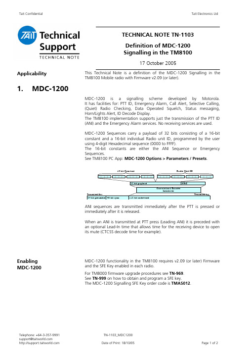
TECHNICAL NOTE TN-1103Definition of MDC-1200Signalling in the TM810017 October 2005Applicability This Technical Note is a definition of the MDC-1200 Signalling in theTM8100 Mobile radio with Firmware v2.09 (or later).1. MDC-1200MDC-1200 is a signalling scheme developed by Motorola.It has facilities for: PTT ID, Emergency Alarm, Call Alert, Selective Calling,(Quiet) Radio Checking, Data Operated Squelch, Status messaging,Horn/Lights Alert, ID Decode Display.The TM8100 implementation supports just the transmission of the PTT ID(ANI) and the Emergency Alarm services. No receiving services are used.MDC-1200 Sequences carry a payload of 32 bits consisting of a 16-bitconstant and a 16-bit individual Radio unit ID, programmed by the userusing 4-digit Hexadecimal sequence (0000 to FFFF).The 16-bit constants are either the ANI Sequence or EmergencySequences.See TM8100 PC App: MDC-1200 Options > Parameters / Presets.ANI sequences are transmitted immediately after the PTT is pressed orimmediately after it is released.When an ANI is transmitted at PTT press (Leading ANI) it is preceded withan optional Lead-In time that allows time for the receiving device to openits mute (CTCSS decode time for example).EnablingMDC-1200MDC-1200 functionality in the TM8100 requires v2.09 (or later) Firmwareand the SFE Key enabled in each radio.For TM8000 firmware upgrade procedures see TN-969.See TN-999 on how to obtain and program a SFE key.The MDC-1200 Signalling SFE Key order code is TMAS012.Telephone: +64-3-357-9991 TN-1103_MDC1200 Date of Print: 18/10/05 Page 1 of 22. ConfigurationSubaudible signalling diagram as it applies to MDC-1200 transmissions.When sending an MDC-1200 sequence the TM8100:• Waits the programmed time Lead-In Delay at the startof a transmission.• Transmits the MDC-1200 sequence including the: 24 bit preamble 48 bit sync 112 bit codeword• A Lead-Out delay at the end of the codeword is then transmitted.Note: This occurs irrespective of whether the transmission is about to stop or not and passes no in-band audio so be wary of setting this too long where it may impact on subsequent user speech.TM8100 MDC-1200 OptionsNOTE : It is not recommended the ANI or Emergency Sequences are changed from the defaults.Parameters ValuesUnits Defaults Lead-In Delay 0 to 5000 (in steps of 10) m/sec 500 Lead-Out Delay 0 to 2500 (in steps of 10) m/secRadio ID 0000 to FFFF Hex 0001 ANI Sequence 0000 to FFFF Hex 8001 Emergency Sequence0000 to FFFFHex 0001Compliance IssuesNone.CSO InstructionInform all sales and service staff and dealers of the released information.3. Issuing AuthorityName and Position of Issuing OfficerGraham BrenchleyTechnical Support EngineerConfidentialityConfidential – This message or document contains proprietary information intended only for the person(s) or organisation(s) to whom it is addressed.All Recipients are legally obliged to not disclose Tait technological or business information to any persons or organisations without the written permission of Tait.Distribution LevelAssociate.Document HistoryOriginal Release17 October 2005GCBTelephone: +64-3-357-9991 TN-1103_MDC1200********************* Date of Print: 18/10/05Page 2 of 2。
8100智能水泵变频器说明书(130-190)-2015-09-08

◎交流输入电源不能接到变频器输出端子 U、V、W 上,否则将导致变频器损坏并且不能 享受保修服务。 ◎不能对变频器进行耐压测试,否则将导致变频器损坏。 ◎变频器的主回路端子配线和控制回路配线应分开布线或垂直交叉,否则将会使控制信 号受干扰。 ◎主回路端子的接线电缆应使用带有绝缘套管的线鼻。 ◎当变频器和电机之间的电缆长度超过 50 米时,建议使用输出电抗器以保护变频器和电 机。
1.2 指示灯说明
◆ 运行:( 常亮 ):运行指示; ( 闪烁 ):休眠停机指示。 ◆ 停止: 停机指示(待机指示)。 ◆ 报警 1:控制器故障报警。 ◆ 报警 2:管网水压异常报警。
- 06 -
8100 系列
1.3 按键操作说明 三级菜单分别为:
① 功能码组号(一级菜单) ② 功能码标号(二级菜单) ③ 功能码设 定值(三级菜单)
8100 系列
目 录
第一章 操作面板说明 .......................06
1.1 操作面板示意图 ..........................06 1.2 指示灯说明 ..............................06 1.3 按键操作说明 ............................07 1.4 压力设置说明 ............................08
- 04 -
■ 运行
8100 系列
◎变频器接线完成并加上盖板后方可通电,严禁带电时拆卸盖板,否则可能导致触电。 ◎当对变频器设置了故障自动复位或停电后自动重启功能时,应预先对设备系统采取安 全保护措施,否则可能导致人员伤害。 ◎“STOP/RESET”(停止 / 复位)按键可能因某功能设置而失效,可在变频器控制系统 中安装一个独立的应急断电开关,否则可能导致人员伤害。 ◎变频器通电后,即使处于停机状态,变频器的端子仍带电,不可触摸,否则有触电危险。
泰特电子TB8100基站连接指南说明书
TB8100 base station Connecting to TB8100 Base Stations via an Asynchronous Port SwitchApplication Note TN-90630 September 2004Contents1The Purpose of an APS . . . . . . . . . . . . . . . . . . . . . . . . . . . . . . . . . . . . . . . 32Supported APS Units and their Main Features. . . . . . . . . . . . . . . . . . . . . . . . 42.1Units Supported. . . . . . . . . . . . . . . . . . . . . . . . . . . . . . . . . . . . . . . . . . . . . . . . . 42.2Main Features . . . . . . . . . . . . . . . . . . . . . . . . . . . . . . . . . . . . . . . . . . . . . . . . . . 4 3Physical Connections. . . . . . . . . . . . . . . . . . . . . . . . . . . . . . . . . . . . . . . . . 54Configuring the Service Kit and Base Station . . . . . . . . . . . . . . . . . . . . . . . . 94.1Configuring the Service Kit for Dial-in via an APS . . . . . . . . . . . . . . . . . . . . . . . 94.2Configuring the Service Kit for a Direct Connection via an APS . . . . . . . . . . . . 114.3Configuring the Base Station to Dial Out to an Alarm Center . . . . . . . . . . . . . . 115Configuring the APS . . . . . . . . . . . . . . . . . . . . . . . . . . . . . . . . . . . . . . . . 135.1Ensuring the Security of Configuration Data . . . . . . . . . . . . . . . . . . . . . . . . . . . 135.2Configuring the Set-up Switches. . . . . . . . . . . . . . . . . . . . . . . . . . . . . . . . . . . . 135.3Configuring the Ports. . . . . . . . . . . . . . . . . . . . . . . . . . . . . . . . . . . . . . . . . . . . 14 6Testing the Connection . . . . . . . . . . . . . . . . . . . . . . . . . . . . . . . . . . . . . . 17 7Essential Modem Features. . . . . . . . . . . . . . . . . . . . . . . . . . . . . . . . . . . . . 18 8Known Issues or Limitations. . . . . . . . . . . . . . . . . . . . . . . . . . . . . . . . . . . 18 Document Conventions‘Configure > Communications > Alarm Center’ means ‘click theConfigure icon on the toolbar, then in the navigation pane find theCommunications group, and select Alarm Center from it’.Associated DocumentationTN-742: Remotely Monitoring and Configuring the TB8100 Base StationTB8100 Installation and Operation ManualTB8100 Service Kit and Alarm Center User’s Manuals and online HelpY our APS User’s GuidePage 2 of 20TN-906© Tait Electronics Limited 30 September 2004This Application Note provides information on how to connect multipleTB8100 base stations to a Service Kit or Alarm Center using anAsynchronous Port Switch (APS). It covers connection via direct serial link,and via PSTN lines using modems. T ypical physical connections, APSconfigurations, base station configurations, Service Kit configurations, andmodem settings are also described.1The Purpose of an APSOne of the most powerful features of the TB8100 base station is its abilityto be remotely configured and monitored. This feature includes Service Kitaccess, for remote configuration, monitoring, and diagnostics, andautomatic dial-out to an Alarm Center, as a result of an error condition orTask Manager stimulus. TN-742 describes the use of this feature in detail.Without using an APS, however, a dedicated PSTN line is required for eachbase station installed on a site. The cost of these lines is very high, especiallywhen the base stations are installed in remote locations. Using an APSallows a single phone line to service up to 31 base stations.A typical connection scenario is shown in Figure1 below. The diagramshows:I four base stations connected to various ports on an APSI the dial-up modem at the remote siteI the PSTN connectionI the modem at the local siteI a PC running either Service Kit or Alarm Center software.Figure 1Typical APS ConnectionTN-906Page 3 of 20© Tait Electronics Limited 30 September 2004Page 4 of 20TN-906© Tait Electronics Limited 30 September 20042Supported APS Units and their Main Features2.1Units SupportedThe APS support feature in the TB8100 base station is intended to work with third party products. Tait Electronics Limited does not manufacture its own unit. The following third party units are supported:IW estern T elematic Inc. (WTI) APS-4, APS-8, APS-16, CMS-16, and CMS-32IBlack Box SW543A.Any other APS that uses simple ASCII connect and disconnect commands and responses may work satisfactorily.2.2Main FeaturesThese features are standard on the supported APS units listed above.IY ou can connect up to 3, 7, 15, or 31 base stations per site to a single PSTN line or PC, depending on the APS chosen.I The units are configured as DTE (Data T erminal Equipment).IThe units will support all baud rates recognised by the base station, i.e. 1200, 2400, 9600, 19200, 38400, 57600, and 115200.IAlthough the APS ports can be individually configured, and may be password protected, the TB8100 base station does not support this. (Note that in “Common Configuration for all Ports” on page 14 the password is left undefined)I The APS configurations are stored in non-volatile memory.IData clashes are prevented using a Busy response, i.e. if one base station tries to dial out while another is connected, it will receive a Busy response, and can try again later if configured to do so.IThe Service Kit or base station alarm dial-out software handle allcommon errors such as busy, lack of response, or communications failure.IThe APS can be powered from 115/230VAC or –48VDC. The power consumption is approximately 5W .3Physical ConnectionsIn all the following connection types, only two or three base stations areshown connected to the APS for graphical convenience.The modem is shown connected to the highest numbered port of the APS.This is for user convenience only, and allows an easy mapping between thebase station number and port number when configuring the Service Kit.Any port could be used if desired.A single null modem cable is supplied with the APS. The user must supplyall other cables.Figure 2PSTN connection to base stations without a TaitNet RS-232 system interface boardTN-906Page 5 of 20© Tait Electronics Limited 30 September 2004Figure 3PSTN connection to base stations with a TaitNet RS-232 system interface boardPage 6 of 20TN-906© Tait Electronics Limited 30 September 2004Figure 4Direct connection to base stations with or without a TaitNet RS-232 system interface boardTN-906Page 7 of 20© Tait Electronics Limited 30 September 2004Figure 5Combined PSTN and direct connectionsPage 8 of 20TN-906© Tait Electronics Limited 30 September 2004TN-906Page 9 of 20© Tait Electronics Limited 30 September 20044Configuring the Service Kit and Base Station4.1Configuring the Service Kit for Dial-in via an APS1.Run the Service Kit and select Connect > New Connection. The Edit Connection screen appears.2.In the Connection type list, select Modem Dialup. The Edit Connection screen changes to the one shown below.Page 10 of 20TN-906© Tait Electronics Limited 30 September 20043.Set up the parameters in the Connection tab as usual (use the online Help if required).4.In the Port Switch tab, select the Port switch check box.5.In the Connect command field, enter ^M/Cx^M.This means:Note Use the ^ (carat) symbol to instruct the Service Kit that this is a control character. Do not use the control key.6.In the Connect response field, enter 1.7.In the Disconnect command field, enter ^Mxxx^M/X^M.This means:8.In the Disconnect response field, enter 3.^M instructs the APS to enter command mode a a.This is equivalent to the carriage return character./C requests a connectionx the port number of the base station you wish to connect to ^Mterminates the sequence^M instructs the APS to enter command mode xxx three instances of the logoff character a a.This must match the logoff character chosen when setting up the modem (L was chosen in this case). Refer to “Common Configuration for all Ports” on page 14.^M terminates the sequence /X^Mexits command mode4.2Configuring the Service Kit for a Direct Connection via an APSThis configuration is similar to the one described in the previous section, except that you set the Connection type to Direct Connection. Y ou can then connect the computer running the Service Kit software to any spare port on the APS, and connect to any base station that is not currently busy with either a dial-in or dial-out session.4.3Configuring the Base Station to Dial Out to an Alarm CenterThis section provides details on configuring the Alarm Center connection, the port switch, and the connection timing. For full details on configuring the modem, refer to TN-742.1.Run the Service Kit and select Configure > Communications > Alarm Center.2.In the Alarm Center form, enable the Alarm Center connection and the Port switch (use the on-line Help if required).3.In the Baud rate list, select 57600. If you select a different baud rate, ensure that the APS is set to the same rate (refer to “Configuring the Set-up Switches” on page 13).4.In the Connect command field, enter ^M/Cx^M.This means:The site modem is usually (but does not have to be) connected to the highest port number available. The above screen shows the settings for port 8 of an 8-port APS.^M instructs the APS to enter command mode a a.This is equivalent to the carriage return character./C requests a connectionx the port number to which the site modem is connected ^Mterminates the sequencePage 12 of 20TN-9065.In the Connect response field, enter 1.6.In the Disconnect command field, enter ^Mxxx^M/X^M.This means:7.In the Disconnect response field, enter 3.8.In the Connection timing area, we recommend the following settings:I Set the number of retries to 20, the maximum allowed.ISet the time between retries to 60s for the first base station, and increment in steps of 5s for other base stations (e.g. set base station 2 to 65s, base station 3 to 70s, etc.). This prevents all base stations from retrying at the same time if a fault occurs that affects them all.ISet the minimum interval to at least 30 minutes. The interval should be long enough to allow all base stations to dial out if necessary; we suggest 30 minutes plus an extra 3 minutes for each base station on the site.NoteIf there is a particular condition that can be guaranteed to affect all base stations (e.g. mains failure), we recommend that you enable this alarm on only two base stations. This precaution will prevent a mass dial-out attempt, but will still allow you to check for false alarms.^M instructs the APS to enter command mode xxx three instances of the logoff character a a.This must match the logoff character chosen when setting up the modem (L was chosen in this case). Refer to “Common Configuration for all Ports” on page 14.^M terminates the sequence /X^Mexits command mode5Configuring the APS5.1Ensuring the Security of Configuration DataThe configuration data of many APS units is stored in RAM which has abattery back-up. This battery should have a life of approximately 3 yearswhen the APS is not powered up, and may need to be changed periodically.Y ou may also wish to replace the battery before installing your APS to ensuremaximum battery life and security of configuration data. A typical symptomof battery failure is the loss of configuration data when the APS is powereddown for some time.The battery is typically a BR1225 and is located under a clip on the mainboard of the APS. T o replace the battery, proceed as follows:1.Disconnect the AC mains power.2.Remove the top cover.3.Carefully replace the battery, observing normal antistatic precautions.4.Replace the cover.5.2Configuring the Set-up Switches1.Power up the APS.2.Configure the set-up switches as shown below. These switches arelocated on the rear panel of APS units with up to 8 ports, and on thebottom cover of units with 16 or more ports.Switch Setting FunctionSW1ON (down)sets the baud rate to 57k6SW2OFFSW3OFFSW4OFF no handshakingSW5OFFSW6OFF terse messagesSW7OFF echo disabledSW8–––currently not usedThe settings for SW1, SW2, and SW3 are optional, however the set-tings for all other switches are mandatory. W e recommend a baud rateof 57k6, as it will give the highest possible data transfer rate throughthe modem on a “good” PSTN connection. If you select a differentrate, you must select the same rate for the Alarm Center connection(Configure > Alarm Center > Port Settings > Baud rate; refer to“Configuring the Base Station to Dial Out to an Alarm Center” onpage11).3.After you have set the switches, you must validate the set-up asfollows:a.Simultaneously press the SET and CLEAR buttons on the front ofthe APS.b.Release the CLEAR button, wait for the port ACTIVITY LEDsto flash, then release the SET button.5.3Configuring the PortsConnect a PC running a terminal program (HyperT erminal, ProComm,T erraT erm or similar) to any unused port on the APS, using a null modemcable.Note Refer to the APS User’s Guide for a detailed explanation of all thecommand codes. The commands shown in the following sectionare in upper case for clarity, however you can use lower case if youprefer.Common Configuration for all Ports 1.Enter Command Mode using the [Enter] key.2.Type the following commands:/CP [Enter]copies port parameters7 [Enter] 1 [Enter]sets all ports to Any-to-Any mode9 [Enter] x [Enter]where x sets the logoff characterNote that this must be the same character youchose in the Service Kit procedures describedin Section4.1 and Section4.3 (L in theexamples shown). It must also be differentfrom the character used to take the modemout of data mode, which is usually “+”, butcan be changed by the user. You can alsochoose control characters, which are shown bya preceding ^ (carat).10 [Enter] 1 [Enter]sets the disconnect sequence to 3 consecutivelogoff characters, instead of just 1Note that this is essential to avoid thepossibility of random logoffs.11 [Enter] 6 [Enter]enables the timeout to 1 minute12 [Enter] 3 [Enter]sets the response type to Terse13 [Enter] 1 [Enter]disables the command echo[Esc]copies to all portsY [Enter]answers the question “Are you sure (y/n)?”/W [Enter]displays port parametersPage 14 of 20TN-9063.V erify that the following is displayed.PORT PARAMETERS #01:1. Port Name: (undefined)2. Password: (undefined)3. Baud Rate: 57.6K4. Bits/Parity: 8-None5. Stop Bits: 16. Handshake Mode: None7. Port Mode: Any-to-Any74. DTR Output: Pulse8. Supervisor Mode: Permit9. Logoff Character: L10. Sequence Disconnect: Three Characters11. Timeout Disconnect: 1 Min12. Response Type: Terse13. Command Echo: Off14. Accept Break: YesIf everything is correct, proceed to step 4, or re-enter the incorrect parameter as required.4.WTI APS-4, APS-8 and APS-16 Units OnlyThis step is required because of a bug in the firmware of the APS-4, APS-8 and APS-16 units. The Copy Port Parameters command does not work for the timeout setting.T ype the following commands:/Pn [Enter]sets RS-232 parameterswhere n is the port number11 [Enter] 6 [Enter]enables the timeout to 1 minute[Esc]Repeat this procedure for all ports.5.If you do not want to configure a port as a modem port (refer to“Configuration for a Modem Port (if a modem is used)” below), exit Command mode by typing:/X [Enter]exits command modeOtherwise, continue with “Configuration for a Modem Port (if amodem is used)” on page16.Configuration for a Modem Port(if a modem is used)W e recommend that you configure the port to which the modem is connected as a modem port. This will ensure that the modem is re-configured after a power outage, and prevent it from using the wrong serial baud rate.T ype the following commands:/Pn [Enter]sets RS-232 parameterswhere n is the number of the port to whichthe modem is connected, usually the highestnumbered portVerify that the timeout has been set correctlyto 1 minute. If not, type 11 [Enter] 6 [Enter].7 [Enter] 4 [Enter]configures the port as a modem port71 [Enter] AT [Enter]sets the reset string to AT72 [Enter] AT [Enter]sets the initialisation string to ATThis is just to ensure that no unwantedcommands are issued to the modem.73 [Enter] +++~~ATH0[Enter]ensures that modem hangs up after a timeoutNote that the double ~ (tilde) puts a 2s delaybetween +++ and ATH0, allowing the modemto enter command mode.[Esc]/X [Enter]exits Command modePage 16 of 20TN-9066Testing the ConnectionConnecting to the Base Station via the APS Once everything has been configured, dial in to the base station via the APS.1.Run the Service Kit software and click Connect.2.Select the APS connection previously set up. The following screenappears, as for a normal (non-APS) connection.Once the modems have connected and established their protocol, the following screen appears. This screen is unique to APS connections.Shortly afterwards, the correct port is connected, and the base station responds to its connection protocol. The normal base station logon screen now appears.3.Continue with the connection session as normal.4.When you have completed your session, disconnect in the normalway.Page 18 of 20TN-906If the Connection is Unsuccessful1.If an error occurs which is related to the APS, the following screen will appear.2.If this screen appears, check the settings of both the APS and the Service Kit very carefully. If the you cannot resolve the problem, it may be useful to insert a serial communications monitor between the Service Kit PC and the modem. Compare the strings actually transmitted with those expected, and consult the APS User’s Guide.7Essential Modem FeaturesThe ATX0 command must be available in any modem which is used with the APS. This command limits the result codes to 0-4, i.e:I 0 – OK I 1 – connect I 2 – ring I 3 – no carrier I4 – errorNoteSome modems will include result code 8 (no answer) in the list for ATX0. This is also acceptable. Refer to TN-742 for modem set-tings and configurations.8Known Issues or LimitationsKnown Issue or LimitationSolutionSome APS units store their configuration data in RAM with battery back-up. This data will be lost if the unit is powered down and the battery fails.If you are unsure about the condition of the back-up battery, replace it before installing the APS (refer to “Ensuring the Security of Configuration Data” on page 13).Applies to WTI APS-4, APS-8 and APS-16 units:You cannot use the Copy Port Parameterscommand to set the timeout.You must set the port timeout on each port individually. If you try to set this parameter globally, it will appear to be successful, but the timeout will not work. Refer to“Common Configuration for all Ports” on page 14.Issuing AuthorityThis TN was issued by:John CrosslandT echnical Publications ManagerPublication HistoryAmendment RecordTait Contact InformationCorporate Head OfficeNew ZealandTait Electronics Limited, P .O. Box 1645, Christchurch, New Zealand E-mail (Marketing): *********************E-mail (Sales): *******************Technical SupportT echnical Support ManagerTait Electronics Ltd, P .O. Box 1645, Christchurch, New Zealand E-mail: *********************InternetPublication Date Author 30 September 2004D ReynoldsPublication Date PageAmendment 30 September 2004First releasePage 20 of 20TN-906。
泰特电子TB8100基站与外部模块连接指南说明书

TB8100 base station Using a TB8100 with an External ModemApplication Note TN-1114-AN21 December 2005Contents1Overview . . . . . . . . . . . . . . . . . . . . . . . . . . . . . . . . . . . . . . . . . . . . . . . . . 3 2Applicability. . . . . . . . . . . . . . . . . . . . . . . . . . . . . . . . . . . . . . . . . . . . . . . 3 3Disclaimer . . . . . . . . . . . . . . . . . . . . . . . . . . . . . . . . . . . . . . . . . . . . . . . . 3 4Functional Description. . . . . . . . . . . . . . . . . . . . . . . . . . . . . . . . . . . . . . . . 4 5Connecting the TB8100 to an External Modem. . . . . . . . . . . . . . . . . . . . . . . 5 6Configuring the Base Station. . . . . . . . . . . . . . . . . . . . . . . . . . . . . . . . . . . . 7 7Performance Specifications. . . . . . . . . . . . . . . . . . . . . . . . . . . . . . . . . . . . . 8 8Frequency Response Graphs . . . . . . . . . . . . . . . . . . . . . . . . . . . . . . . . . . . . 9 Associated DocumentationTB8100 Installation and Operation Manual (MBA-00005-xx).TB8100 Specifications Manual (MBA-00001-xx).TB8100 Service Kit User’s Manual (MBA-00010-xx) and online Help.Y our modem User’s Guide.Page 2 of 10TN-1114-AN© Tait Electronics Limited 21 December 2005TN-1114-ANPage 3 of 10© Tait Electronics Limited 21 December 20051OverviewThis Application Note provides information on how to configure a TB8100base station to use an external modem by means of the extended bypassaudio functionality. The extended bypass functionality provides an analoguesignal path with a higher than standard frequency response, but only via theunbalanced line. This allows the connection of external modems that haveinformation content above 3kHz. Included in this Application Note areinstructions on how to configure the TB8100, and some performanceindications for various types of modem.This Application Note is intended for use by system integrators.2ApplicabilityThe extended bypass audio functionality is only available on reciters withhardware version 0.04 or later. The performance has been tested using onlythe unbalanced line interface on an isolated system interface board(TBA10B0).Note The TB8100 does not check the extended bypass functionalityagainst the hardware version number. It is up to the user to ensurethat the correct hardware version is used.3DisclaimerTait Electronics Limited has not applied for, and will not apply for,regulatory compliance when using the bypass or extended bypass path. Thisis because Tait does not want to specify any particular external modem to beused. The choice of external modem is therefore up to the user.The bypass and extended bypass path has been provided to facilitate only adata path through the TB8100. Note that normal voice-type compliancescannot be achieved when this has been selected in the channel profile. Thisis primarily due to the lack of a limiter in the transmit modulation path.It is therefore the responsibility of the user to apply to their local regulatoryauthorities for the appropriate data compliances.Page 4 of 10TN-1114-AN© Tait Electronics Limited 21 December 20054Functional DescriptionExciter BypassThe bypass path connects the audio sampled at 25kHz from the analogue unbalanced line input directly into the frequency control loop (FCL), which then modulates the RF hardware. The only digital filtering in the bypass path is an optional AC filter, which has a cut-off frequency of 0.8Hz. Note that there is no limiter present in this path.Receiver BypassOn the receive audio bypass path, received audio from the FM demodulator is decimated from 50kHz to 25kHz. It is then directly converted to the analogue unbalanced line output with no further filtering. Extended BypassThere is anti-alias analogue filtering performed on the unbalanced lines, and also on the FCL outputs. This filtering on the bypass path causes a roll-off in amplitude as the audio frequency is increased. When extended bypass is enabled, the analogue filtering on the unbalanced lines is disabled by hardware, and a digital finite impulse response filter with a constant group delay is used in both the transmit and receive bypass paths to extend the frequency response.TN-1114-ANPage 5 of 10© Tait Electronics Limited 21 December 20055Connecting the TB8100 to an External ModemConnection Connect the TB8100 to the external modem using the unbalanced lineinput (Tx audio) and output (Rx audio) on the system interface connector.If required, you can also use the Rx Gate and Tx Key lines, as describedbelow.Details of the pin allocations for the different types of system interfaceconnector are provided in the “Connection” chapter in the TB8100Installation and Operation Manual, and also in the TB8100 Service Kit(Configure > Base Station > System Interface).AC Coupled Unbalanced Audio Input The modem selected may have a DC offset present for both the transmitter and the receiver. On the standard system interface board, the transmit pathis DC coupled (with a bias of 2.5V), and the receive path is AC coupled.W e recommend that you enable the high pass filter in the Signal Path tab ofthe channel profile dialogue box in the Service Kit (refer to “Configuringthe Base Station” on page 7). This will ensure that the transmitted signal isexactly on the configured carrier frequency. If you do not enable the highpass filter, ensure that you set the transmit carrier frequency exactly to therequired frequency by adjusting the DC bias of the external modem.Note The CODECs used to sample the unbalanced line input are DCcapable. However, because of component variations, the DCoffset incorrectly reported by the CODEC can lead to a smalloffset in the transmit carrier frequency, which is removed byselecting the high pass filter.Figure 1Typical connectionPage 6 of 10TN-1114-AN© Tait Electronics Limited 21 December 2005Receiver Gating If the receiver is not gated, the received audio will be continuously presented to the external modem. This may lead to the occasional false packet detection, due to noise falsing the decoder. One option to prevent this is to gate the received audio and/or use the Rx Gate signal to indicate to the modem when a valid RF signal is present. Note In this case, you will probably have to configure the external modem to cope with the timing sequence of audio presented from the unbalanced line. Refer to the TB8100 Specifications Manual for gating response times.Tx KeyIf you do not require continuous transmission, you can use the Tx Key input on the system interface board to key up the TB8100, and to key it down when transmission is not required. Note In this case, you will probably have to configure the external modem to cope with the timing sequence of audio presented to the unbalanced line for transmission. W e also recommend that you refer to the Tx Timers tab of the signalling profile dialogue box in the Service Kit, and select suitable values or disable timersas appropriate for your system.TN-1114-ANPage 7 of 10© Tait Electronics Limited 21 December 20056Configuring the Base StationExtended bypass is configured in the channel profile assigned to theoperating channel. If a different operating channel is selected, the signalpath configured for that channel will take effect.Important Selecting this function bypasses the limiter. This may allowoverdeviation and cause the equipment to become non-compliant. It should be selected only when the TB8100 isconnected to approved level-controlled devices (modems,trunking controllers, etc.).ImportantWith extended bypass you cannot use the balanced line orinternal talk-through repeater connections from receiver totransmitter.T o configure the signal path for extended bypass.1.Run the Service Kit and open the Add or Edit Channel Profile dia-logue box for the appropriate profile.2.Select the Signal Path tab.3.Select the Bypass check boxes for Path B (both transmit and receive).Extended bypass check boxes appear alongside the Bypass checkboxes.Page 8 of 10TN-1114-AN© Tait Electronics Limited 21 December 20054.Select one of the Extended bypass check boxes. This selects theother Extended bypass check box as well. (Y ou cannot configureextended bypass separately for the transmit and receive paths.)7Performance SpecificationsExtended bypass has been tested with external modems as follows:The performance figures given in these specifications are typical, and aresupplied only as a guide to the expected performance. The actualperformance achieved by your system will depend on the specific externalmodem used, and the interface levels into the TB8100.narrow bandwidth C4FM9600bps external modem based on a CML FX919 chipset narrow bandwidth GMSKBT=0.5, 4800bps external modem based on a CML FX489 chipset wide bandwidth GMSK BT=0.5, 9600bpsexternal modem based on a CML FX489 chipsetNB C4FMNB GMSK WB GMSK Minimum Receiver RF Level for a Robust Link ––a –109dBm(0.79µV)–109dBm (0.79µV)Strong Signal Packet Error Rate (PER)**for RF levels of 0dBm <10-4<10-4<10-4Signal Displacement Bandwidth>1kHz >1kHz >2kHz Selectivity ––a 71dB 79dB Modulation Fidelity**measured as Error Vector Magnitude, through combinedreceive and transmit paths3.5%6%6%a.Unavailable at time of publication.TN-1114-ANPage 9 of 10© Tait Electronics Limited 21 December 2005Publication InformationIssuing Authority This TN was issued by:Kurt EbrechtT echnical Publications ManagerDistribution Level Associate, Associate System Integrator, Accredited Service Centre,Accredited Service Centre System Integrator, or Tait Only .Publication History Amendment Record Tait Contact InformationCorporate Head Office New Zealand Tait Electronics Limited, P .O. Box 1645, Christchurch, New Zealand E-mail (Marketing): *********************E-mail (Sales): *******************Technical Support T echnical Support ManagerTait Electronics Ltd, P .O. Box 1645, Christchurch, New ZealandE-mail: *********************Internet Publication DateAuthor 21 December 2005 D Reynolds Publication DatePage Amendment 21 December 2005First releasePage 10 of 10TN-1114-AN© Tait Electronics Limited 21 December 2005。
UC-8100A-ME-T Series 硬件用户手册说明书

UC-8100A-ME-T Series Hardware User’sManualVersion 1.0, April 2019/product© 2019 Moxa Inc. All rights reserved.UC-8100A-ME-T Series Hardware User’sManualThe software described in this manual is furnished under a license agreement and may be used only in accordance withthe terms of that agreement.Copyright Notice© 2019 Moxa Inc. All rights reserved.TrademarksThe MOXA logo is a registered trademark of Moxa Inc.All other trademarks or registered marks in this manual belong to their respective manufacturers.DisclaimerInformation in this document is subject to change without notice and does not represent a commitment on the part of Moxa.Moxa provides this document as is, without warranty of any kind, either expressed or implied, including, but not limited to, its particular purpose. Moxa reserves the right to make improvements and/or changes to this manual, or to the products and/or the programs described in this manual, at any time.Information provided in this manual is intended to be accurate and reliable. However, Moxa assumes no responsibility for its use, or for any infringements on the rights of third parties that may result from its use.This product might include unintentional technical or typographical errors. Changes are periodically made to the information herein to correct such errors, and these changes are incorporated into new editions of the publication.Technical Support Contact Information/supportMoxa AmericasToll-free: 1-888-669-2872 Tel: +1-714-528-6777 Fax: +1-714-528-6778Moxa China (Shanghai office) Toll-free: 800-820-5036Tel: +86-21-5258-9955 Fax: +86-21-5258-5505Moxa EuropeTel: +49-89-3 70 03 99-0 Fax: +49-89-3 70 03 99-99Moxa Asia-PacificTel: +886-2-8919-1230 Fax: +886-2-8919-1231Moxa IndiaTel: +91-80-4172-9088 Fax: +91-80-4132-1045Table of Contents1.Introduction ...................................................................................................................................... 1-1Model Descriptions .............................................................................................................................. 1-2 Package Checklist ............................................................................................................................... 1-2 Product Features ................................................................................................................................ 1-2 Product Specifications ......................................................................................................................... 1-2 2.Hardware Introduction...................................................................................................................... 2-1Appearance ........................................................................................................................................ 2-2 Dimensions ........................................................................................................................................ 2-3 LED Indicators .................................................................................................................................... 2-4 Reboot .............................................................................................................................................. 2-4 Reset to Default ................................................................................................................................. 2-4 Real-time Clock .................................................................................................................................. 2-5 Installation Options ............................................................................................................................. 2-5 DIN-rail Mounting ........................................................................................................................ 2-5Optional Wall Mounting ................................................................................................................ 2-6 3.Hardware Connection Description ..................................................................................................... 3-1Wiring Requirements ........................................................................................................................... 3-2 Connecting the Power .................................................................................................................. 3-2Grounding the Unit ...................................................................................................................... 3-2 Connecting to the Network ................................................................................................................... 3-3 Connecting to a USB Device ................................................................................................................. 3-3 Connecting to Serial Ports .................................................................................................................... 3-3 Inserting the SD Card and SIM Card ..................................................................................................... 3-3 Connecting to the Console Port ............................................................................................................. 3-4 Connecting the Antennas ..................................................................................................................... 3-4 A.Regulatory Approval Statements ....................................................................................................... A-11Introduction The UC-8100A-ME-T computing platform is designed for embedded data-acquisition applications. TheUC-8100A-ME-T platform comes with two RS-232/422/485 serial ports and dual 10/100 Mbps Ethernet LAN ports, as well as a miniPCIe slot to support cellular modules. These versatile communication capabilities let users efficiently adapt the UC-8100A-ME-T to a variety of complex communications solutions.The following topics are covered in this chapter:❒Model Descriptions❒Package Checklist❒Product Features❒Product SpecificationsUC-8100A-ME-T Series HW UM IntroductionModel DescriptionsThe UC-8100A-ME-T Series includes the following models:•UC-8112A-ME-T-LX: Industrial computing platform with 2 serial ports, 2 Ethernet ports, SD socket, -40 to 85°C operating temperature range•UC-8112A-ME-T-LX-US: Industrial computing platform with 2 serial ports, 2 Ethernet ports, SD socket, US region LTE built-in,-40 to 70°C operating temperature range•UC-8112A-ME-T-LX-EU: Industrial computing platform with 2 serial ports, 2 Ethernet ports, SD socket, Europe region LTE built-in,-40 to 70°C operating temperature range•UC-8112A-ME-T-LX-AP: Industrial computing platform with 2 serial ports, 2 Ethernet ports, SD socket, APAC region LTE built-in,-40 to 70°C operating temperature rangePackage ChecklistBefore installing a UC-8100A-ME-T computer, verify that the package contains the following items:•UC-8100A-ME-T Series computer•Console cable•Power jack•Quick Installation Guide (printed)•Warranty cardNotify your sales representative if any of the above items are missing or damaged.NOTE The console cable and power jack can be found beneath the molded pulp cushioning inside the product box.Product Features•Armv7 Cortex-A8 1 GHz processor• 2 auto-sensing 10/100 Mbps Ethernet ports•SD socket for storage expansion•Programmable LEDs and a programmable button for easy installation and maintenance•Mini PCIe socket for cellular module•Debian 9 open platform•-40 to 70°C wide temperature range with LTE enabledProduct SpecificationsNOTE The latest specifications for Moxa's products can be found at https://.2Hardware Introduction The UC-8100A-ME-T embedded computers are compact and rugged, making them suitable for industrial applications. The LED indicators allow you to monitor device performance and quickly identify issues, and the multiple ports can be used to connect a variety of devices. The UC-8100A-ME-T Series comes with a reliable and stable hardware platform that lets you devote the bulk of your time to application development. In this chapter, we provide basic information about the embedded computer’s hardware and its various components. The following topics are covered in this chapter:❒Appearance❒Dimensions❒LED Indicators❒Reboot❒Reset to Default❒Real-time Clock❒Installation OptionsD IN-rail MountingO ptional Wall MountingAppearanceTop ViewFront ViewBottom ViewDimensionsUnit: mm (in)LED IndicatorsThe function of each LED is described in the table below:LED Name Color FunctionUSB GreenSteady OnUSB device is connected and working normally.Off USB device is not connected.SD GreenSteady On SD Card inserted and working normally.Off SD card is not detected.PowerGreen Power is on and the computer is working normally.OffPower is off.LAN1/LAN 2(RJ45connector)GreenSteady On 100 Mbps Ethernet linkBlinking Data transmission in progressYellowSteady On 10 Mbps Ethernet linkBlinking Data transmission in progressOffEthernet is not connected.Wireless SignalStrengthGreenYellowRedThe number of glowing LEDs indicates the signal strength.3 (Green + Yellow + Red): Excellent2 (Yellow + Red): Good1 (Red): PoorOff Wireless module is not detected.USR User-defined GreenThis LED can be defined by users. For details, refer to HardwareUser’s Manual.Programmablediagnostic LEDsGreenYellowRedThese three LEDs are programmable. For details, refer to the“Default Programmable Button Operation" section in the HardwareUser’s Manual.RebootTo reboot the computer, press the programmable button for 1 second.Reset to DefaultThe UC-8100A-ME-T is also provided with a Reset to Default function which can reset the operating systemback to the factory default status. Press and hold the programmable button between 7 to 9 seconds to resetthe computer to the factory default settings. When the reset button is held down, the Ready LED will blink onceevery second. The Ready LED will become steady when you hold the button continuously for 7 to 9 seconds.Release the button within this period to load the factory default settings.Real-time ClockThe UC-8100A-ME-T’s real time clock is powered by a non-chargeable battery. We strongly recommend that you do not replace the lithium battery without help from a qualified Moxa support engineer. If you need to change the battery, contact the Moxa RMA service team.Installation OptionsDIN-rail MountingThe aluminum DIN-rail attachment plate is already attached to the product’s casing. To mount theUC-8100A-ME-T on to a DIN rail, make sure that the stiff metal spring is facing upwards and follow these steps.1.Pull down the bottom slider of the DIN-railbracket located at the back of the unit 2. Insert the top of the DIN rail into the slot justbelow the upper hook of the DIN-rail bracket. 3. Latch the unit firmly on to the DIN rail as shown inthe illustrations below.4. Push the slider back into place.UC-8100A-ME-T Series HW UM Hardware IntroductionOptional Wall MountingThe UC-8100A-ME-T can be mounted on to a wall using a wall-mounting kit as shown in the following illustrations. Step 1Use four screws to fasten the wall-mounting brackets on the left panel of the computer.Step 2Use another four screws to mount the computer on a wall or a cabinet.The optional wall-mounting kit is not included in the product box and should be purchased separately.3 Hardware Connection DescriptionIn this chapter, we describe how to connect the UC-8100A-ME-T to a network and various devices.The following topics are covered in this chapter:❒Wiring RequirementsC onnecting the PowerG rounding the Unit❒Connecting to the Network❒Connecting to a USB Device❒Connecting to Serial Ports❒Inserting the SD Card and SIM Card❒Connecting to the Console Port❒Connecting the AntennasWiring RequirementsIn this section, we describe how to connect various devices to the embedded computer. Be sure to read and follow these common safety precautions before proceeding with the installation of any electronic device: • Use separate paths to route wiring for power and devices. If power wiring and device wiring paths mustcross, make sure the wires are perpendicular at the intersection point.NOTEDo not run signal or communication wiring and power wiring in the same wire conduit. To avoid interference, wires with different signal characteristics should be routed separately.• You can use the type of signal transmitted through a wire to determine which wires should be kept separate.The rule of thumb is that wiring that shares similar electrical characteristics can be bundled together. • Keep input wiring and output wiring separate.• When necessary, it is strongly advised that you label wiring to all devices in the system.Connecting the PowerTerminal BlockConnect the 12 to 36 VDC power line to the terminal block, which is connector to the UC-8100A-ME-T Series computer. If the power is supplied properly, the “Power” LED will glow a solid green light. The power input location and pin definition are shown in the adjacent diagram.SG: The Shielded Ground (sometimes called Protected Ground) contact is the bottomcontact of the 3-pin power terminal block connector when viewed from the angle shown here. Connect the SG wire to an appropriate grounded metal surface.Grounding the UnitThere is another grounding connector on the top panel of the computer. Use this connector to connect a well-grounded mounting surface, such as a metal panel.Connecting to the NetworkThe Ethernet ports are located on the front panel of the UC-8100A-ME-T computers. The pin assignments for the Ethernet port are shown in the following figure. If you are using your own cable, make sure that the pin assignments on the Ethernet cable connector match the pin assignments on the Ethernet port.Pin Signal 1 Tx+ 2 Tx- 3 Rx+ 4– 5 – 6 Rx- 7 – 8–Connecting to a USB DeviceThe UC-8100A-ME-T Series computers come with a USB port located at the lower part of the front panel, allowing users to connect to a device with an USB interface. The USB port uses a type A connector. By default, the USB storage is mounted at /mnt/usbstorage.Connecting to Serial PortsThe two serial ports (P1 and P2) use terminal connectors. Each port can be configured by software for RS-232, RS-422, or RS-485. The pin assignments for the ports are shown in the following table:Pin RS-232 RS-422RS-485 1 TXD TXD+ – 2 RXD TXD- – 3 RTS RXD+ D+ 4 CTS RXD- D- 5GNDGNDGNDInserting the SD Card and SIM CardThe UC-8100A-ME-T comes with an SD socket for storage expansion, and a SIM card socket for cellular communication. The SD card/SIM card sockets are located at the lower part on the front panel. To install the cards, remove the screw and the protection cover to access the sockets, and then insert the SD card or the SIM card into the sockets directly. You will hear a click when the cards are in place. To remove the cards, push the cards in before releasing them.Connecting to the Console PortThe console port is an RS-232 port that can be connected to with a 4-pin pin header cable. You can use this port for debugging or firmware upgrade.PinSignal1 TxD2 RxD3 NC4 GNDConnecting the AntennasThere are three antenna connectors on the front panel of theUC-8100A-ME-T. W1 and W3 are for cellular modules, and W2 isfor GPS module; all are SMA type. Connect the antennas on theseconnectors.ARegulatory Approval StatementsThis device complies with part 15 of the FCC Rules. Operation is subject to the following two conditions: (1) This device may not cause harmful interference, and (2) this device must accept any interference received, including interference that may cause undesired operation.Class A: FCC Warning! This equipment has been tested and found to comply with the limits for a Class A digital device, pursuant to part 15 of the FCC Rules. These limits are designed to provide reasonable protection against harmful interference when the equipment is operated in a commercial environment. This equipment generates, uses, and can radiate radio frequency energy and, if not installed and used in accordance with the instruction manual, may cause harmful interference to radio communications. Operation of this equipment in a residential area is likely to cause harmful interference in which case the users will be required to correct the interference at their own expense.European Community。
013 8100、8200控制屏说明

Logo
8120控制屏说明
主控制器为BE24控制器
科泰电源设备(上海)有限公司
COOLTECH POWER(SHANGHAI)LTD.
Logo
8120控制屏说明
主控制器参量信息
1、低燃油液位报警指示 2、紧急停机报警指示 3、低油压停机报警指示 4、高水温停机报警指示 5、电池电压值 6、皮带断裂/充电发电机故障报警指示 7、超/低频率停机报警指示 8、启动失败停机报警指示 9、交流发电机故障
科泰电源设备(上海)有限公司
COOLTECH POWER(SHANGHAI)LTD.
Logo
8100控制屏说明 8100控制屏(501K) 8100控制屏(501K)电路原理 控制屏
科泰电源设备(上海)有限公司
COOLTECH POWER(SHANGHAI)LTD.
Logo
8120控制屏说明
二、8120控制屏说明 8120控制屏说明
Logo
8100、8120、8200、8220控制屏说明 8100、8120、8200、8220控制屏说明
科泰电源设备(上海)有限公司
—销售服务中心
版本编号:VO.0801-13
Logo
8100、8200控制屏说明 8100、8200控制屏说明 目 录 1、8100控制屏说明 2、8120控制屏说明 3、8200控制屏说明 4、8220控制屏说明 5、KX系列ATS
科泰电源设备(上海)有限公司
COOLTECH POWER(SHANGHAI)LTD.
Logo
8120控制屏说明
控制屏外面板 1.主控制器:整个系统的主控制器; 2.微型空气开关:控制线路过流及短路保护; 3.紧急停机按钮
3
CP8100系列可编程4通道直流电子负载模块用户编程手册

通道 2 的负载工作模式,详细见 2.3.1 节中的表 4。
15 浮点型 0
通道 2 的定负载值或 Vo 值。当负载模式为 CC 模式时,表示定电
流值;当负载模式为 CV 模式时,表示定电压值;当负载模式为
CR 模式时,表示定电阻值;当负载模式为 CP 模式时,表示定功
率值;当负载模式为 LED 模式时,表示 LED 的 Vo 值。
0
整型 0
各种工作模式下的负载输入开关控制寄存器。该寄存器中的低 4
位用于控制 4 个通道的负载输入开关。1 表示输入打开,0 表示输
入关闭。
Bit0:通道 1 负载输入开关
Bit1:通道 2 负载输入开关
Bit2:通道 3 负载输入开关
Bit3:通道 4 负载输入开关
Bit4-Bit15:未定义,系统保留。
CR 模式时,表示定电阻值;当负载模式为 CP 模式时,表示定功
率值;当负载模式为 LED 模式时,表示 LED 的 Vo 值。
3
浮点型 0
通道 1 的 LED 模式中的 Io 值,其他负载模式下无意义,可置 0
4
浮点型 0
通道 1 的 LED 模式中的 Rd 系数,其他负载模式下无意义,可置
0
5
整型 0
1
可编程直流电子负载模块 CP8101 & CP8102 & CP8103 用户编程手册
2
声明
本手册版权归深圳市中科源电子有限公司所有,未经版权所有者同意任何单位、个人 不得复制、传播、翻印、引用本手册的任何内容。
本手册若内容有变更,恕不另行通知。
版本修订记录
日期 2013.08.19 2013.11.28 2014.02.21
- 1、下载文档前请自行甄别文档内容的完整性,平台不提供额外的编辑、内容补充、找答案等附加服务。
- 2、"仅部分预览"的文档,不可在线预览部分如存在完整性等问题,可反馈申请退款(可完整预览的文档不适用该条件!)。
- 3、如文档侵犯您的权益,请联系客服反馈,我们会尽快为您处理(人工客服工作时间:9:00-18:30)。
第四章功能和特性 ........................................................................................................................................ 26
4.1 切换本地/远程操作模式 ..................................................................................................................... 26 4.2 定态操作模式 ..................................................................................................................................... 26
1.3.1 安装尺寸 ...................................................................................................................................... 6 1.3.2 负载手柄的调节 ......................................................................................................................... 12 1.3.3 支架安装 .................................................................................................................................... 13 1.4 输入连接部分的安装 ......................................................................................................................... 14
2.1 开机自检 ............................................................................................................................................ 15 2.1.1 介绍 ............................................................................................................................................ 15 2.1.2 自检步骤..................................................................................................................................... 15 2.1.3 如果负载不能启动 ...................................................................................................................... 16
2.2 前面板介绍 ........................................................................................................................................ 17 2.3 后面板介绍......................................................................................................................................... 18 2.4 VFD 状态指示灯功能描述 .................................................................................................................. 19 2.5 键盘介绍 ............................................................................................................................................ 19 2.6 快速功能键......................................................................................................................................... 20
第二章 技术规格......................................................................................................................................... 21
3.1 主要技术参数 ..................................................................................................................................... 21 3.2 补充参数 ............................................................................................................................................ 25
TH8100 使用手册
用户使用手册
直流可编程电子载
TH8100系列
型号TH8101/TH8103/ TH8103A/ TH8103B/TH8106/TH8115/TH8130
© 版权归属于同惠电子股份有限公司 Ver2.7/FEB,2014/TH8100-2011
1
用户使用手册
目录
TH8100 使用手册
第二章快速入门............................................................................................................................................ 15
第一章 验货与安装 ....................................................................................................................................... 6
1.1 验货 ..................................................................................................................................................... 6 1.2 清洁 ..................................................................................................................................................... 6 1.3 安装位置.............................................................................................................................................. 6
4.2.1 定电流操作模式(CC) .................................................................................................................. 27 4.2.2 定电压操作模式(CV) .................................................................................................................. 27 4.2.3 定电阻操作模式(CR) .................................................................................................................. 27 4.2.4 定功率操作模式(CW) ................................................................................................................. 28 4.3 输入控制 ..................................................................