十八、运放容性负载问题
运算放大器驱动容性负载
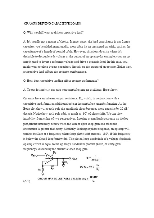
OP AMPS DRIVING CAPACITIVE LOADSQ.Why would I want to drive a capacitive load?A.It's usually not a matter of choice.In most cases,the load capacitance is not from a capacitor you've added intentionally;most often it's an unwanted parasitic,such as the capacitance of a length of coaxial cable.However,situations do arise where it's desirable to decouple a dc voltage at the output of an op amp-for example,when an op amp is used to invert a reference voltage and drive a dynamic load.In this case,you might want to place bypass capacitors directly on the output of an op amp.Either way, a capacitive load affects the op amp's performance.Q.How does capacitive loading affect op amp performance?A.To put it simply,it can turn your amplifier into an oscillator.Here's how:Op amps have an inherent output resistance,R o,which,in conjunction with a capacitive load,forms an additional pole in the amplifier's transfer function.As the Bode plot shows,at each pole the amplitude slope becomes more negative by20dB/ decade.Notice how each pole adds as much as-90°of phase shift.We can view instability from either of two perspectives.Looking at amplitude response on the log plot,circuit instability occurs when the sum of open-loop gain and feedback attenuation is greater than unity.Similarly,looking at phase response,an op amp will tend to oscillate at a frequency where loop phase shift exceeds-180°,if this frequency is below the closed-loop bandwidth.The closed-loop bandwidth of a voltage-feedback op amp circuit is equal to the op amp's bandwidth product(GBP,or unity-gain frequency),divided by the circuit's closed loop gain(A CL).Phase margin of an op amp circuit can be thought of as the amount of additional phase shift at the closed loop bandwidth required to make the circuit unstable(i.e.,phase shift+phase margin=-180°).As phase margin approaches zero,the loop phase shift approaches-180°and the op amp circuit approaches instability.Typically,values of phase margin much less than45°can cause problems such as"peaking"in frequency response,and overshoot or"ringing"in step response.In order to maintain conservative phase margin,the pole generated by capacitive loading should be at least a decade above the circuit's closed loop bandwidth.When it is not,consider the possibility of instability.Q.So how do I deal with a capacitive load?A.First of all you should determine whether the op amp can safely drive the load on its own.Many op amp data sheets specify a"capacitive load drive capability".Others provide typical data on"small-signal overshoot vs.capacitive load".In looking at these figures,you'll see that the overshoot increases exponentially with added load capacitance.As it approaches100%,the op amp approaches instability.If possible, keep it well away from this limit.Also notice that this graph is for a specified gain. For a voltage feedback op amp,capacitive load drive capability increasesproportionally with gain.So aVF op amp that can safely drive a100-pF capacitance at unity gain should be able to drive a1000-pF capacitance at a gain of10.A few op amp data sheets specify the open loop output resistance(R o),from which you can calculate the frequency of gain-the added pole as described above.The circuit will be stable if the frequency of the added pole(f P)is more than a decade above the circuit's bandwidth.If the op amp's data sheet doesn't specify capacitive load drive or open loop output resistance,and has no graph of overshoot versus capacitive load,then to assure stability you must assume that any load capacitance will require some sort of compensa-tion technique.There are many approaches to stabilizing standard op amp circuits to drive capacitive loads.Here are a few:Noise-gain manipulation:A powerful way to maintain stability in low-frequency applications-often overlooked by designers-involves increasing the circuit'sclosed-loop gain(a/k/a"noise gain")without changing signal gain,thus reducing the frequency at which the product of open-loop gain and feedback attenuation goes to unity.Some circuits to achieve this,by connecting RD between the op amp inputs,are shown below.The"noise gain"of these circuits can be arrived at by the givenequation.Since stability is governed by noise gain rather than by signal gain,the above circuits allow increased stability without affecting signal gain.Simply keep the"noisebandwidth"(GBP/A NOISE)at least a decade below the load generated pole to guaranteestability.One disadvantage of this method of stabilization is the additional output noise and offset voltage caused by increased amplification of input-referred voltage noise and input offset voltage.The added dc offset can be eliminated by including C D in series with R D,but the added noise is inherent with this technique.The effective noise gain of these circuits with and without C D are shown in the figure.C D,when used,should be as large as feasible;its minimum value should be10A NOISE/(2pR D GBP)to keep the"noise pole"at least a decade below the"noise bandwidth".Out-of-loop compensation:Another way to stabilize an op amp for capacitive load drive is by adding a resistor,RX,between the op amp's output terminal and the load capacitance,as shown below.Though apparently outside the feedback loop,it acts with the load capacitor to introduce a zero into the transfer function of the feedback network,thereby reducing the loop phase shift at high frequencies.To ensure stability,the value of R X should be such that the added zero(f Z)is at least a decade below the closed loop bandwidth of the op amp circuit.With the addition of R X,circuit performance will not suffer the increased output noise of the first method, but the output impedance as seen by the load will increase.This can decrease signal gain,due to the resistor divider formed by R X and R L.If R L is known and reasonably constant,the results of gain loss can be offset by increasing the gain of the op amp circuit.This method is very effective in driving transmission lines.The values of R L andR X must equal the characteristic impedance of the cable(often50ohms or75ohms)in order to avoid standing waves.So R X is pre-determined,and all that remains is to double the gain of the amplifier in order to offset the signal loss from the resistor divider.Problem solved.In-loop compensation:If R L is either unknown or dynamic,the effective output resistance of the gain stage must be kept low.In this circumstance,it may be useful to connect R X inside the overall feedback loop,as shown below.With this configuration,dc and low-frequency feedback comes from the load itself,allowing the signal gain from input to load to remain unaffected by the voltage divider,R X andR L.The added capacitor,C F,in this circuit allows cancellation of the pole and zero contributed by C L.To put it simply,the zero from C F is coincident with the pole from C L,and the pole from C F with the zero from C L.Therefore,the overall transfer function and phase response are exactly as if there were no capacitance at all.In order to assure cancellation of both pole/zero combinations,the above equations must be solved accurately.Also note the conditions;they are easily met if the load resistance is relatively large.Calculation is difficult when R O is unknown.In this case,the design procedure turns into a guessing game-and a prototyping nightmare.A word of caution about SPICE:SPICE models of op amps don't accurately model open-loop output resistance (RO);so they cannot fully replace empirical design of the compensation network.It is also important to note that C L must be of a known(and constant)value in order for this technique to be applicable.In many applications,the amplifier is driving a load"outside the box,"and C L can vary significantly from one load to the next.It is best to use the above circuit only when C L is part of a closed system.One such application involves the buffering or inverting of a reference voltage, driving a large decoupling capacitor.Here,C L is a fixed value,allowing accurate cancellation of pole/zero combinations.The low dc output impedance and low noise of this method(compared to the previous two)can be very beneficial.Furthermore, the large amount of capacitance likely to decouple a reference voltage(often many microfarads)is impractical to compensate by any other method.All three of the above compensation techniques have advantages and disadvantages. You should know enough by now to decide which is best for your application.Allthree are intended to be applied to "standard",unity gain stable,voltage feedback op amps.Read on to find out about some techniques using special purpose amplifiers.Q.My op amp has a "compensation"pin.Can I overcompensate the op amp so that it will remain stable when driving a capacitive load?A.Yes.This is the easiest way of all to compensate for load capacitance.Most op amps today are internally compensated for unity-gain stability and therefore do not offer the option to "overcompensate".But many devices still exist with inherent stability only at very high noise gains.These op amps have a pin to which an external capacitor can be connected in order to reduce the frequency of the dominant pole.To operate stably at lower gains,increased capacitance must be tied to this pin to reduce the gain-bandwidth product.When a capacitive load must be driven,a further increase (overcompensation)can increase stability 裝ut at the expense of bandwidth.Q.So far you've only discussed voltage feedback op amps exclusively,right?Do current feedback (CF)op amps behave similarly with capacitive loading?Can I use any of the compensation techniques discussed here?A.Some characteristics of current feedback architectures require special attention when driving capacitive loads,but the overall effect on the circuit is the same.The added pole,in conjunction with op-amp output resistance,increases phase shift and reduces phase margin,potentially causing peaking,ringing,or even oscillation.However,since a CF op amp can't be said to have a "gain-bandwidth product"(bandwidth is much less dependent on gain),stability can't be substantially increased simply by increasing the noise gain.This makes the first method impractical.Also,a capacitor (C F )should NEVER be put in the feedback loop of a CF op amp,nullifying the third method.The most direct way to compensate a current feedback op amp to drive a capacitive load is the addition of an "out of loop"series resistor at theamplifier output as in method 2.Part Number ChBW MHz SR V/ms v n nV/Hzi n fA/H zV OSmVI bnASupply Voltage Range [V]I Q mA R O ohms CapLoad Drive [pF]NotesAD8171503501515000.530005-3678unlim AD8262503501515000.530005-366.88unlimAD8272503001515000.530009-36 5.2515unlimAD8471503001515000.530009-36 4.815unlimAD848135200515000.530009-36 5.115unlim G MIN=5 AD849129200315000.330009-36 5.115unlim G MIN=25 AD70440.80.1515500.030.14-360.37510000AD70510.80.1515500.030.064-360.3810000AD70620.80.1515500.030.054-360.37510000OP9710.90.214200.030.034-400.3810000OP2792532210004300 4.5-1222210000OP40040.50.15116000.080.756-400.610000AD549113350.220.50.0001510-360.64000OP20020.50.15114000.080.16-400.572000OP467428170680000.21509-3621600AD7441137516100.30.039-36 3.51000comp.term AD8013314010003.51200023000 4.5-13 3.41000current fb AD85322353050250.0053-6 1.41000AD85344353050250.0053-6 1.41000OP2718 2.8 3.217000.03158-44 6.7701000OP3711217 3.217000.03158-44 6.7701000GMIN=5 OP27025 2.4 3.211000.05159-3621000OP470462 3.217000.4259-36 2.251000OP27529226150011009-4421000OP1841 4.254 3.94000.18804-3621000OP2842 4.254 3.94000.18804-3621000OP4844 4.254 3.94000.25804-3621000OP19310.041565500.15203-360.031000OP29320.041565500.25203-360.031000Q.This has been informative,but I'd rather not deal with any of these equations. Besides,my board is already laid out,and I don't want to scrap this production run.Are there any op amps that are inherently stable when driving capacitive loads?A.Yes.Analog Devices makes a handful of op amps that drive"unlimited"load capacitance while retaining excellent phase margin.They are listed in the table,alongwith some other op amps that can drive capacitive loads up to specified values.Aboutthe"unlimited"cap load drive devices:don't expect to get the same slew rate when driving10µF as you do when driving purely resistive loads.Read the data sheets for details.。
运放及其典型电路

All rights reserved 版权所有,仿冒必究 Company Confidential 公司机密,不得公开
运放基本应用—比较器
带参考电压的滞回比较器电路 如下图(a)所示,同相输入端的电位为: 令uI=uN=uP,求出的uI就是阈值电压,因此得出: 当UREF>0V时,电路的传输特性如图(b)所示。
常用电路分类--环路控制(9) 环路控制(9)
双环控制
All rights reserved 版权所有,仿冒必究 Company Confidential 公司机密,不得公开
目录
运放基本应用
运放两个工作区 正/反相比例放大电路 加/减法电路 比较器电路
运放的常规应用 运放使用的一些注意事项 案例分享
All rights reserved 版权所有,仿冒必究 Company Confidential 公司机密,不得公开
运放基本应用--加/减法电路 加/减法电路
加/减法电路注意事项 为了减小偏置电流对电路的影响,运放同相输 入端和反相输入端的外围等效电阻应该相等。 电阻R1,R2和R3的阻值尽量在1千欧到1兆 欧之间选取,取值过大或过小,均可能给电路带 来负面影响。
All rights reserved 版权所有,仿冒必究 Company Confidential 公司机密,不得公开
运放基本应用--正/反相比例放大电路 正/反相比例放大电路
同相比例运算放大电路 计算关系如下: vo=(1+R3/R2)*vi; 同相比例放大电路的特点: 同相比例放大电路的输出信号与输 入信号同相,输出电压的大小与电 阻1+R3/R1值成比例。 偏置/补偿电阻R1取值近似为电阻 R2和R3的并联等效电阻。 电阻R1,R2和R3的阻值尽量在1千 欧到1兆欧之间选取,取值过大或过 小,均可能给电路带来负面影响。
“驯服”振荡—电容性负载问题
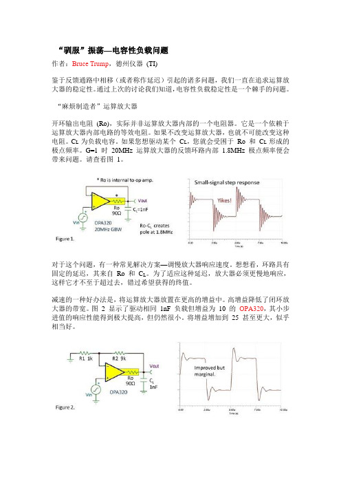
“驯服”振荡—电容性负载问题作者:Bruce Trump,德州仪器(TI)鉴于反馈通路中相移(或者称作延迟)引起的诸多问题,我们一直在追求运算放大器的稳定性。
通过上次的讨论我们知道,电容性负载稳定性是一个棘手的问题。
“麻烦制造者”运算放大器开环输出电阻(Ro),实际并非运算放大器内部的一个电阻器。
它是一个依赖于运算放大器内部电路的等效电阻。
如果不改变运算放大器,也就不可能改变这种电阻。
C L 为负载电容。
如果您想驱动某个C L,您就会受困于Ro 和C L 形成的极点频率。
G=1 时20MHz 运算放大器的反馈环路内部 1.8MHz 极点频率便会带来问题。
请查看图1。
对于这个问题,有一种常见解决方案—调慢放大器响应速度。
想想看,环路具有固定的延迟,其来自Ro 和C L。
为了适应这种延迟,放大器必须更慢地响应,这样它才不至于超过去,错过希望获得的终值。
减速的一种好办法是,将运算放大器放置在更高的增益中。
高增益降低了闭环放大器的带宽。
图 2 显示了驱动相同1nF 负载但增益为10 的OPA320,其小步进值的响应性能得到极大提高,但仍然很小。
将增益增加到25 甚至更大,似乎相当好。
但是另一个问题出现了。
图 3 增益仍为10,但增加了Cc,其将速度又降低了1 位。
Cc 过小时,响应看起来更像图2。
Cc 过大时,可能出现问题,其看起来更像图1。
恰到好处地补偿,可解决“靠近速率”问题——Bode图分析。
这已经超出一篇博客文章所能讨论的范围了,因此我只能试着给您一些建议。
在解决这些问题时,可以借助于您的直觉,但是如果您提高补偿操作的能力水平,那么就需要向Bode 先生(Bode图)请教了。
我以前的同事Tim Green,写过一个关于运算放大器稳定性和Bode图分析的系列文章。
另外,我的同事Collin Wells也发表过许多精辟的见解。
如果您想深入了解,我强烈建议您首先观看文章后面的Collin讲座。
另外,如果您够幸运的话,您还可以在TI 技术研讨会现场观看他的讲座。
ADI_1218_TW运放的容性负载的稳定性
18
19
Solution2-- Out Of Loop Compensation
Adding
a resistor(Rx) between the op amp’s output terminal and the load capacitance Introduce a zero into the transfer function of the feedback network, thereby reducing the loop phase shift at high frequencies. Disadvantage
ቤተ መጻሕፍቲ ባይዱ
15
Simulation Result ---- Phase Margin = 66.8°
16
The World Leader in High Performance Signal Processing Solutions
Solutions
Solution1-- Increasing the closed-loop gain
graph of “small-signal overshoot vs. capacitive load” shows the relations between the overshoot and added load capacitance. The bigger the overshoot, the worse the stability. The graph is for a specified gain. A voltage feedback amp that can safely drive a 100-pF capacitance at unity gain should be able to drive a 1000-pF capacitance at a gain of 10.
运放输出端口有大电容负载的补偿方法
运放输出端口有大电容负载的补偿方法1. 增加模拟电路的稳定性和响应速度是处理运放输出端口大电容负载的关键挑战之一。
2. 为了解决这一问题,可以使用零极点补偿技术,其中在运放的反馈回路内引入零点和极点,以稳定输出电路并降低阶跃响应的过冲和振荡。
3. 另一种方法是使用毛切斯稳定器(Tsu75或Tsu77),它是一种特殊的负反馈网络,可提供额外的相位裕度和频率稳定性,有助于应对大电容负载的挑战。
4. 采用多级增益放大器设计,以降低输出阻抗,提高电路的带宽和稳定性。
5. 通过添加补偿电容或电感来抵消输出电路中由大电容负载引起的相位延迟,以维持系统的稳定性。
6. 采用交叉耦合技术,通过在反馈网络中引入动态阻抗来抑制大电容负载引起的相位失真。
7. 使用交叉耦合电容,它可以在运放输出端口和负载之间提供补偿,以保持系统的稳定性和性能。
8. 结合布朗基环和米勒效应进行动态补偿,以提高输出端口对大电容负载的稳定性。
9. 选择合适的运放器件,例如具有高输出驱动能力和过载保护特性的运放器件,以适应大电容负载的需求。
10. 采用主动低通滤波器,以抑制运放输出端口大电容负载引起的高频振荡和干扰。
11. 使用低ESR电解电容或固体电解电容,以提供电源隔离和稳定性,降低大电容负载对系统的影响。
12. 采用带有内部电流限制器和短路保护功能的运放器件,以降低输出端口面对大电容负载时的不稳定性。
13. 使用防护电路和稳压器来保护运放器件免受大电容负载的过载和瞬态冲击。
14. 结合软启动电路,以减缓输出端口对大电容负载的启动过程,降低系统压陷和过载风险。
15. 采用恒流充电器或限流电路,以控制输出端口对大电容负载的充电过程,提高系统的稳定性和可靠性。
16. 定制输出级功率放大器的设计,以匹配大电容负载的电流需求,保证系统的动态响应和稳定性。
17. 采用有源电流源和差分对输入,以降低运放输出端口面对大电容负载时的共模噪声和失真。
18. 设计有效的磁化电流补偿电路,以处理大电感负载对运放器件的影响,提高系统的稳定性和性能。
【分享】“可恶”的运算放大器电容负载
【分享】“可恶”的运算放大器电容负载他们说如果使用放大器驱动电容负载(图1、CLOAD),一个不错的经验是采用一个 50 或 100 欧的电阻器 (RISO) 将放大器与电容器隔开。
这个附加电阻器可能会阻止运算放大器振荡。
图1.支持电容负载的放大器可能需要在放大器输出与负载电容器之间连接一个电阻器。
使用50 或100 欧姆(RISO) 电阻不一定每次都管用。
问题是,“如果CLOAD 超过产品说明书中推荐的运算放大器电容负载值时该怎么办?”如果您无法找到任何说明书指导,或您的负载电容 (CLOAD) 确实超过了产品说明书推荐值,那问题的答案就要取决于:放大器增益带宽积(GBWP 或 fU)放大器的开环输出电阻 (RO)电容器负载值 (CLOAD)图 1 中的频率与增益图显示了当 RISO 和 CLOAD 加到放大器输出端时放大器开环增益曲线的情况。
如果使用这三个变量,您就可以计算出适当的 RISO 值。
下面是确定 RISO 值时的规则:(公式 1)(公式 2)这两个规则可确保电路的稳定。
适合这一概念的应用是将输入驱动至 SAR-ADC。
在这种情况下,需要该信号在转换器的采集时间内 (tACQ) 内稳定。
公式 3 中的 K 是ADC 时间常数乘法器,其可提供半 LSB 的高精度。
对于 ADS7886 等16 位转换器而言,K 等于 11.78。
(公式 3)我们来应用这些公式,采用以下参数进行计算:对于 OPA365fU = 50 MHzR0 = 30 欧姆增益 = 1 V/V对于 ADS7886tACQ = 300 nsCIN = 21 pFCLOAD = 390 pFOPA365 产品说明书显示,100 pF 的负载会产生 30% 的过冲(图2)。
图 2. OPA365 过冲与电容负载公式 1、2 和 3 可帮助解决该过冲问题。
公式 1,RISO => 3.33 欧姆公式 2,RISO => 30.97 欧姆公式 3,RISO ~ 61.96 欧姆鉴于这三个公式,RISO 必须等于 61.9 欧姆(0.1% 容差)。
十八、运放容性负载问题
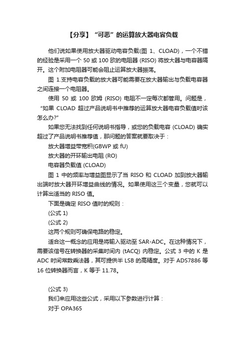
十八、运放容性负载问题18 运算放大器容性负载驱动问题Grayso n King,Analog Device s Inc.问:为什么我要考虑驱动容性负载问题?答:通常这是无法选择的。
在大多数情况下,负载电容并非人为地所加电容。
它常常是人们不希望的一种客观存在,例如一段同轴电缆所表现出的电容效应。
但是在有些情况下,要求对运算放大器的输出端的直流电压进行去耦。
例如,当运放被用作基准电压的倒相或驱动一个动态负载时。
在这种情况下,你也许在运放的输出端直接连接旁路电容。
不论哪种情况,容性负载都要对运放的性能有影响。
问:容性负载如何影响运放的性能?答:为简单起见,可将放大器看成一个振荡器。
每个运放都有一个内部输出电阻RO,当它与容性负载相接时,在运放传递函数上产生一个附加的极点。
正如图1(b)波特图幅频特性曲线表示,附加极点的幅频特性斜率比主极点20dB/十倍频程更徒。
从相频特性曲线图1(c)中可以看出,每个附加极点的相移都增加-90°。
我们可用图1(b)或图1(c)来判断电路的稳定性。
从图1(b)中可以看出,当开环增益和反馈衰减之和大于1时,电路会不稳定。
同样,在图1(c)中,如果某一工作频率低于闭环带宽,在这个频率下环路相移超过-180°时,运放会出现振荡。
电压反馈型运算放大器(VFA)的闭环带宽等于运放增益带宽积(GBP,或单位增益频率)除以电路闭环增益(A CL )。
运算放大器电路的相位裕度定义为使电路不稳定所要求的闭环带宽处对应的附加相移(即环路相移十相位裕度=-180°)。
当相位裕度为0时,环路相移为-180°,此运放电路不稳定。
通常,当相位裕度小于45°时,会出现问题,例如频响“尖峰”,阶跃响应中的过冲或“振铃”。
容性负载
容性负载电路中类似电容的负载,可以使电流超前电压降低电路功率因数一般把带电容参数的负载,即符合电压滞后电流特性的负载称为容性负载。
充放电时,电压不能突变。
其对应的功率因数为负值。
对应的感性负载的功率因数为正值。
在高频领域,是指负载虚部为负值的负载.容性负载:和电源相比,负载电流超前负载电压一个相位差,此时负载为容性负载(如补偿电容负载)。
一般电源控制类产品,所给出的负载,如未加说明则是给出的是视在功率,即总容量功率;它既包括有功功率,也包括无功功率;而一般感性负载说明中给出的往往是有功功率的大小,例如荧光灯,标注为15~40瓦的荧光灯,镇流器消耗功率约为8瓦,实际在考虑用定时器,感应开关在控制它时,则要加上这8瓦;具体不同的产品感性部分,即无功功率的大小,可以通过其给出的功率因数来计算。
混联电路中,若容抗比感抗大,电路呈容性,反之为感性。
通常的用电器中并没有纯感性负载和纯容性负载。
因为这两种负载不做有用功。
只有在补偿电路中才使用纯感性负载或纯容性负载。
又因为绝大多数负载除阻性外,多数为感性负载,因此补偿的时候多数就用电容来补偿,所以,纯容性负载用得比纯感性负载多。
如电动机,变压器等等,通常为感性负载。
部分日光灯为容性负载。
举例:纯感性负载就是一组电感。
通常用来补偿电路中的容性电流。
在电路中带线圈的用电设备,其线圈部分即为纯感性负载。
如电动机、变压器、电风扇、日光灯镇流器等。
纯感性负载的电流是不能突变(楞次定律)。
感性负载应用广泛。
在电路中带电容的用电设备,其电容部分即为纯容性负载。
如补偿电容等。
纯感性负载的电流是不能突变。
从理论上讲:纯电阻电路、纯电容电路、纯电感电路是不存在的。
电阻负载在作功时也会有电感、电容性负载存在。
例如:导线间会存在线路间的电容,导线间和对地间存在电感,期间感性负载通常大于容性负载。
电力电容在作功时也会发热,即电阻性作功。
电感亦如此。
元件的阻抗是频率的函数。
在全频率范围内纯电阻电路、纯电容电路、纯电感电路是不存在的。
- 1、下载文档前请自行甄别文档内容的完整性,平台不提供额外的编辑、内容补充、找答案等附加服务。
- 2、"仅部分预览"的文档,不可在线预览部分如存在完整性等问题,可反馈申请退款(可完整预览的文档不适用该条件!)。
- 3、如文档侵犯您的权益,请联系客服反馈,我们会尽快为您处理(人工客服工作时间:9:00-18:30)。
十八、运放容性负载问题
18 运算放大器容性负载驱动问题
Grayson King,Analog Devices Inc.
问:为什么我要考虑驱动容性负载问题?
答:通常这是无法选择的。
在大多数情况下,负载电容并非人为地所加电容。
它常常是人们不希望的一种客观存在,例如一段同轴电缆所表现出的电容效应。
但是在有些情况下,要求对运算放大器的输出端的直流电压进行去耦。
例如,当运放被用作基准电压的倒相或驱动一个动态负载时。
在这种情况下,你也许在运放的输出端直接连接旁路电容。
不论哪种情况,容性负载都要对运放的性能有影响。
问:容性负载如何影响运放的性能?
答:为简单起见,可将放大器看成一个振荡器。
每个运放都有一个内部输出电阻RO,当它与容性负载相接时,在运放传递函数上产生一个附加的极点。
正如图1(b)波特图幅频特性曲线表示,附加极点的幅频特性
斜率比主极点20dB/十倍频程更徒。
从相频特性曲线图1(c)中可以看出,每个附加极点的相移都增加-90°。
我们可用图1(b)或图1(c)来判断电路的稳定性。
从图1(b)中可以看出,当开环增益和反馈衰减之和大于1时,电路会不稳定。
同样,在图1(c)中,如果某一工作频率低于闭环带宽,在这个频率下环路相移超过-180°时,运放会出现振荡。
电压反馈型运算放大器(VFA)的闭环带宽等于运放增益带宽积(GBP,或单位增益频率)除以电路闭环增益(A CL )。
运算放大器电路的相位裕度定义为使电路不稳定所要求的闭环带宽处对应的附加相移(即环路相移十相位裕度=-180°)。
当相位裕度为0时,环路相移为-180°,此运放电路不稳定。
通
常,当相位裕度小于45°时,会出现问题,例如频响“尖峰”,阶跃响应中的过冲或“振铃”。
为了使相位裕度留有余地,容性负载产生的附加极点至少应比电路的闭环带宽高10倍,如果不是这样电路可能不稳定。
问:那么我应该如何处理容性负载?
答:首先我们应该确定运放是否能稳定地驱动自身负载。
许多运放数据手册都给出“容性负载驱动能力”这项指标。
还有一些运放提供“小信号过冲与容性负载关系曲线”,从中你可以看到过冲与附加负载电容呈指数关系增加,当达到100%时,运放不稳定。
如果有
可能,应该使运放过冲远离100%。
还应注意这条曲线对应指定增益。
对于VFA,容性负载驱动能力随增益成比例增加。
所以,如果在增益为1时,VFA可稳定驱动100pF容性负载,那么在增益为10时,便能驱动1000pF容性负载。
也有少数运放的产品说明中给出开环输出电阻RO,从而可以计算出上述附加极点的频率fP= 1/2πROCL。
如果附加极点fP大于上述电路带宽10倍,则电路稳定。
如果运放的产品说明没有提供容性负载驱动能力或开环输出电阻的指标,也没有给出过冲与容性负载关系曲线,那么要保证电路稳定,你必须对容性负载采取必要的补偿措施。
要使标准运放驱动容负载工作稳定有许多处理方法,下面介绍几种。
(1)提高噪声增益法
使低频电路稳定的有效方法,也是设计者常常忽略的方法,就是增加电路的闭环增益(即噪声增益),而不改变信号增益,这样可在开环增益与反馈衰减到0dB带宽之积恒定条件下降低噪声带宽。
具体电路如图2所示。
在图2(a)中,在运放的两个输入端之间接电阻RD。
此时电路的增益可由给定公式计算。
因为是噪声增益而不是信号增益支配稳定性,所以电路稳定性的提高不影响信号增益。
为保证电路稳定,最简单的方法是使噪声带宽至少应比容性负载极点频率低10倍频程。
图3 环路增益波特图
这种方法的缺点是输入端电压噪声和输入失调电压被放大产生附加的输出电压噪声和输出失调电压增加。
用一个电容CD与电阻RD串联可以消除附加的直流失调电压,但增加的电压噪声是器件固有的,不能消
除。
当选用CD时,其电容值应尽可能大。
为保证噪声极点至少低于“噪声带宽”10倍,CD最小应取
10A NOISE /2πRDGBP。
(2)环路外补偿法
这种方法是在运放的输出端和负载电容之间串入一个电阻RX,如图4所示。
虽然RX加在反馈环路的外部,但它可将负载电容产生的附加零点频率fZ作用到反馈网络的传递函数,从而可以减小高频环路相移。
为了保证电路稳定,RX的取值应该使附加零点频率至少比运放电路闭环带宽低10倍。
电路加入RX使电路性能不会像方法1那样增加输出噪声,但是从负载端看进去的输出阻抗要增加。
由于RX和RL构成分压器,从而会使信号增益降低。
如果RL已知并且适当地恒定,那么增益降低值可通提高运放电路的增益来补偿。
这种方法用于驱动传输线路非常有用。
RL和RX值必须等于电缆的特征阻抗(通常为50Ω和75Ω),以免产生驻波。
因此,先确定RX值,其余其它电阻值要使放大器的增益加倍,用来补偿由电阻分压作用降低的信号增益,从而解决问题。
(3)环路内补偿法
如果RL值未知,或者是动态值,那么增益级的有效输出电阻必须很低。
在这种情况下,在整个反馈环路
内接一个电阻RX是很有用的,如图5所示。
在这个电路中,由于直流和低频反馈都是来自负载电阻RL,所以从输入端到负载的信号增益不受分压器RX和RL的影响。
图5 环路内补偿法
RX=RORGRF
CF=RO+RXRF·CL
在这个电路中外接的电容CF是用来抵消CL产生的附加极点和零点。
为了简便起见,CF产生的零点频率应该与CL产生的极点频率相一致,CF产生的极点频率应该与CL产生的零点频率相一致。
因此整个传递函数和相频响应好像似没有电容作用一样。
为了确保极点和零点作用相互抵消,图5中的方程必须求解准确。
还应注意方程成立的条件:RF RO,RG RO,RL RO。
如果负载电阻很大,这些条件容易满足。
当RO未知时,计算则很困难。
在这种情况下,设计过程变成猜谜游戏。
应该注意“SPICE”这个词:运算放大器的SPICE模型是一种不能精确地表示运放开环输出电阻RO的模型,所以这种模型不能完全取代传统的补偿网络设计方法。
还应当强调指出的是,为了采用这种方法,CL必须已知(且为常数)。
在许多应用中,放大器驱动一个电路外部的负载,当负载改换时,CL也应该适当变化。
只有当CL接入闭环系统时,使用上述电路才最适合。
这种在基准电压的缓冲器或倒相器中,驱动一个大的去耦电容。
这里CL是固定值,可以精确地抵消极点和零点的作用。
与前两种方法相比,这种方法非常适合用于低直流输出电阻和低噪声的情况。
而且像对基准电压源进行去耦的那么大的容性负载(一般几微法),用其它方法补偿都是不切实际的。
上述三种补偿方法都各有其优点和缺点。
为了对你的应用做出最好的选择,应该对它们有足够的认识。
这三种方法都适合用于“标准”用法,即单位增益稳定,电压反馈运算放大器(VFA)。
对于特殊应用的放大器,读者应该采用其它方法。
问:我的运放有一个“补偿”脚。
当驱动容性负载时,为使电路保持稳定,我能用它对运放进行补偿吗?
答:可以。
这是对容性负载进行补偿的最简单的方法。
现在许多运放都带有使单位增益稳定的内部补偿电路。
但是许多运放只有在很高噪声增益下才能一直保持固有的稳定性。
这类运放有一个与外部电容相连的引脚,用来减少主极点频率。
为了在低增益时工作稳定,外接电容必须靠近这个引脚,以减小增益带宽积。
当驱动容性负载时,增加外接电容过补偿)可以提高稳定性,但是带宽降低。
问:到现在为止,你只讨论了VFA的容性负载驱动问题,是吗?那么对于电流反馈运算放大器(CFA)的容性负载驱动问题应如何处理?上述讨论的那些方法,我可以使用吗?
答:当驱动容性负载时,对CFA的一些特性要特别注意,但容性负载对电路的影响是相同的。
与运放输出电阻相连的容性负载产生附加极点,从而增加相移并降低相位裕度,有可能产生尖峰、振铃,甚至振荡。
但是,因为CFA不存在增益带宽积这个概念(带宽依赖于增益的程度很小),所以通过简单增加噪声增益的方法,对提高电路稳定性没有显著作用。
这样便使第一种方法失效。
另外,电容绝不应接入CFA反馈环路,这样又使第三种方法失效。
对驱动容性负载的CFA进行补偿最合适的方法是方法2,在环路外串接一个电阻。
问:你上述介绍了一些很有用的方法,但是我还不能处理容性负载驱动问题。
另外,我的印制线路板已经制好,并且不想报废。
请问是否有驱动容性负载自身很稳定的运放?
答:有。
ADI公司提供一些很有用的运放,它们既能驱动“无限制”容性负载,同时又能保持优良的相位裕度,如表1所示。
表1还给出了驱动容性负载可高达规定值的另一类运放。
所谓驱动容性负载“无限制”并不是意味着驱动10μF容性负载像驱动阻性负载那样具有相同的转换速率。