TOP246-TOP249系列单片机开关电源应用
TOP244Y单片开关电源原理及维修技巧

TOP244Y单片开关电源原理及维修技巧作者:刘宜新来源:《电子技术与软件工程》2016年第13期摘要本文首先概述了TOP244Y单片开关电源的基本工作原理,接着根据本人多年的维修实践经验,详细介绍了针对此电路的维修技巧,最后通过以TOP244Y单片开关电源维修实例进行剖析,进一步说明TOP244Y开关电源的具体维修技巧及故障的处理。
【关键词】开关电源 TOP244Y单片开关电源原理故障维修技巧开关电源又被称为高效节能电源,它不仅效率高,可达到80﹪-90﹪,而且去掉了笨重的工频变压器,它是利用体积很小的高频变压器来实现电压变换及电网隔离,这样为家用电器的小型化、轻型化奠定了坚实的基础。
采用TOP244Y单片开关电源用途非常广泛,很多民用家用电子产品都采用了此种电路方案,因此家电维修人员很有必要掌握TOP244Y单片开关电源的维修方法。
1 TOP244Y开关电源工作原理分析该开关电源芯片内含脉宽调制器、功率场效应管、自动偏置电路、保护电路。
再配合外部的一次整流滤波电路、、取样比较反馈电路、二次整流滤波电路等部分就组成了一个完整的单片开关电源。
其电路原理如附图所示,以下分别进行分析:1.1 TOP244Y芯片各引脚功能TOP244Y是一款集成式开关电源芯片,它将脉冲宽度调制(PWM)控制系统的全部功能集成到芯片中,其功能引脚如图1所示,各脚功能如下:1.1.1 漏极(D)引脚高压功率MOSFET的漏极输出,通过内部开关高压电流源提供启动偏置电流。
1.1.2 控制(C)引脚误差放大器及反馈电流的输入脚,用于占空比控制。
当控制引脚电压VC接近5.8 V时,控制电路被激活并开始软启动。
当出现开环或短路等故障而使外部电流无法流入控制引脚时,控制引脚上的电容开始放电,达到4.8 V时激活自动重启动电路而关断MOSFET开关管的输出,使控制电路进入低电流的待机模式。
同时该脚也是脉宽调制器电流反馈的控制脚,其占空比与流入控制脚超过芯片内部消耗所需要的电流成反比,实现脉宽调制。
基于TOP249开关电源的设计
0 引 言
开 关 电 源 是 利 用 现 代 电 子 技 术 .控 制 开 关 晶 体 管 开 通 和关 断 的时 间 比率 。维 持稳定 输 出 电压 的一 种 电源 .开 关 电 源 一 般 南 脉 冲 宽 度 调 制 (PW M)和 MOSFET 构 成 。开 关 电源 和线 性 电源 相 比 ,二 者 的成本 都 随着 输 出 功率 的 增加 而 增长 ,但二 者增 长 速率各 异 。开 关 电源 比普 通 的线 性 电源 效率 高 ,开关 电源 的发展 与 应用 在 节约 能 源 、节 约 资 源及 保 护环 境方 面都 具有 重 要 的意 义 。开关 电 源高 频 化 是其 发展 的方 向 ,高频 化使 开关 电 源小 型化 .并使 开 关 电 源进 入更 广泛 的应用 领域 .开 关 电源 比普通 线性 电源 体积 小 ,重 量 轻 ,更便 于 携带 。
1 开 关 电源 未 来 的发 展 方 向
(1)小 型 化 、薄 型 化 、轻 量 化 、高 频 化 。 开 关 电 源 的 体
修 稿 日期 :2016—03—05 作 者 简 介 : 兰 茂龙 (1971-),男 ,讲 师 ,学 士 学位 。研 究方 向 :电 气 自动 化 技 术 。
积 、重 量 主 要 是 南 储 能 元 件 (磁 性 元 件 和 电 容 )决 定 的 ,冈 此 开关 电 源 的小 型化 实质 上 就是 尽可 能 减小 其 中储 能 元 件 的 体积 ;在 一 定 范 围 内 ,开 关 频率 的提 高 ,不 仅 能 有 效 地 减小 电容 、电感及 变 压 器 的尺 寸 ,而且 还 能 够抑 制 干 扰 ,改 善 系统 的 动态 性能 。冈此 ,高频 化 是开 关 电源 的主 要 发 展 方 向 。
基于TOPSwitch-GX系列TOP247Y芯片的低功率开关电源设计

由TOP247Y构成的多路开关电源原理图见图2,其中输出三路200mA、15V的直流电,一路400mA、15V的直流电,以及1A、5V的直流电。多路电源用高频变压器获得多组电压输出,经快速恢复二极管、电容滤波后得到多路直流电源。
当电源输入交流85~265V时,交流电压U依次经过电磁干扰(EMI)滤波器(C1,L1)、输入整流滤波器(KBL406G,C2)获得直流高压UI。UI经过R1接L端,能使极限电流随UI升高而降低。它使用C3,VD型漏极钳位二极管P6KE200A和阻断二极管D1,以替代价格较高的TVS(瞬态电压抑制器),用于吸收在TOP247Y关断时由高频变压器漏感产生的尖峰电压,对漏极起到保护作用。次级电压经过整流、滤波后获得多路输出。其中15V电源输出所用的是快速恢复二极管,其他输出用的二极管是肖特基二极管,其目的是减少整流管的损耗。
由TOP247Y构成的多路开关电源原理图
该电源采用3枚芯片,包括TOP247Y(U1)、光耦合器LTV817A,以及可调式精密并联稳压管LM431。为减小高频变压器体积和增强磁场耦合程度,次级绕组采用了堆叠式绕法。其稳压原理为,U=UR4+UZ+ULM431。当U发生变化时,如U增加时,流过光耦的电流增大,光耦输出的电流随着增大,流经TOP247Y控制端的电流增加,而占空比则减小,从而U下降,这样达到稳压的目的,反之U减小时也有相同的原理。
基于TOPSwitch-GX系列TOP247Y芯片的低功率开关电源设计
本文介绍了一种基于TOP247Y的多路开关稳压电源,其结构简单、成本低廉、制作调试方便,基本上能达到所要求的条件。
TOPSwitch-GX系列芯片工作原理
图1给出了TOP247Y芯片内部结构图,共有6个引出端,它们分别是控制端C、线路检测端L、极限电流设定端X、源极S、开关频率选择端F和漏极D。利用线路检测端(L)可实现4种功能:过压(OV)保护;欠压(UV)保护;电压前馈(当电网电压过低时用来降低最大占空比);远程通/断(ON/OFF)和同步。而利用极限电流设定端,可从外部设定芯片的极限电流。在每个开关周期内都要检测功率MOSFET漏源极导通电阻Ros(on)上的漏极峰值电流ID(PK),当ID(PK)>ILIMIT时,过电流比较器就输出高电平,依次经过触发器、主控门和驱动级,将MOSFET关断,起到过电流保护作用。
top246电源

Power IntegrationsDesign Example ReportTitle21.7 W Power Supply using TOP246P Specification Input: 85 - 265 VAC Output: 48 V / 450 mA Application PoE AC AdapterAuthor Power Integrations Applications Department Document Number DER-97Date September 12, 2005 Revision1.0Summary and Features• Single Sided PC board• Reduced cost and component count • Eliminates two y-capacitors to ground• Eliminates secondary side common mode choke • Eliminates ground wire differential choke • High Efficiency (~ 80 %)• Lower Cost Transformer Construction – no sleeving termination required • Low EMI signature (both radiated and conducted emissions) •Built-in output short circuit protectionThe products and applications illustrated herein (including circuits external to the products and transformer construction) may be covered by one or more U.S. and foreign patents or potentially by pending U.S. and foreign patent applications assigned to Power Integrations. A complete list of Power Integrations’ patents may be found at .Table Of Contents1Introduction (3)2Power Supply Specification (4)3Schematic (5)4Circuit Operation (6)4.1General (6)4.2Description (6)5Bill of Materials (7)6Layout (9)7Transformer Design Spreadsheet (10)8Transformer Specification (13)9Performance (17)9.1Efficiency (17)9.2Regulation vs. Load (18)9.3Regulation vs. Line (19)9.4Raw Performance Data (20)10Waveforms (21)10.1Drain Current and Voltage (21)10.2Output Transient Load Response (22)10.3Output Ripple Voltage (23)10.4Switching Ripple (23)10.5Line Frequency Ripple (24)10.6Output Voltage Shutdown Profile (26)11Thermal Test (27)11.1Thermal Performance (27)12Conducted EMI (29)12.1Conducted EMI Performance (29)13Revision History (30)Important Notes:Although this board is designed to satisfy safety isolation requirements, the engineering prototype has not been agency approved. Therefore, all testing should be performed using an isolated source to provide power to the prototype board.Design Reports contain a power supply design specification, schematic, bill of materials, and transformer documentation. Performance data and typical operation characteristics are included. Typically only a single prototype has been built.1 IntroductionThis document is an engineering report describing a Power over Ethernet (PoE) power supply utilizing TOP246P. The power supply delivers 21.7 W continuous from an input of 85 to 265 VAC.This document provides complete design information including specification, schematic, bill of material and transformer design and construction information. The document also provides performance information.Figure 1 – Circuit Board - Top ViewFigure 2 – Circuit Board - Bottom View2 Power Supply SpecificationDescriptionSymbolMinTypMaxUnitsCommentInputVoltage V IN 85 265 VACOutputOutput Voltage 1V OUT1 47.52 48 48.48 V ± 1% Output Ripple Voltage 1 V RIPPLE1 480 mVp-p 20 MHz bandwidthOutput Current 1 I OUT1 0 450 mA Power Down Holdup115 VAC T H(115VAC) 18 ms 230 VACT H(230VAC)60 msTotal Output PowerAverage Output Power P OUT121.7 WFull Load Efficiency η 80 % EnvironmentalConducted EMIMeets CISPR22B / EN55022BSafety Designed to meet IEC950, UL1950Class IIAmbient Temperature T AMB 0 40 oCForced airflow3 Schematic Figure 3 – Schematic4 Circuit Operation4.1 GeneralThe power supply uses a TOP246P device (U2), with integrated MOSFET and controller, in an isolated flyback configuration. The circuit also uses the x-pin programmable current limit feature control the overload power of the power supply and also to minimize transformer size.4.2 DescriptionThe input fuse F1 protects the supply against catastrophic failure. Thermistor RT1 limits the in-rush current during power-up. Diodes D5 – D8 implement a bridge rectifier to rectify the input mains voltage. Capacitor C22 attenuates the EMI generated by the input bridge diodes D5-D8.Inductor L1 is used to attenuate both differential and common mode EMI noise from the power supply. A large value is used to also prevent any noise filtering through from networks connector to the power supply output. Capacitor C2 forms part of the EMI solution by shunting EMI signals generated across the transformer T2. Capacitor C4 decouples the rectified input voltage providing a DC-bus. Resistor R14 programs the current limit of the TOPSwitch-GX (U2). Resistors R6 and R9 modified this current limit with input voltage, to maintain a relatively flat output overload profile. Diode D2, R2, C1 and R1 implement an RCD clamp circuit to limit the leakage inductance spike on the TOPSwitch-GX Drain pin. Diode D3 and C8 implement a bias voltage supply to provide operating power to the TOPSwitch-GX with integrated PWM, controller and main switching MOSFET. Capacitors C13 and C14 provide device decoupling with C14 also programming the startup and auto-restart period of the device. Resistor R13 provides feedback compensation in conjunction with C14. The inductance of transformer T2 provides the energy storage and conversion component of the circuit. Resistor R41 feeds current to an indicator LED U6, which is illuminated during normal operation.The 48 V output is rectified and filtered by diodes D1 and D4 and capacitors C5 with C7 provided output decoupling. Resistor R18 and C21 snub high frequency ringing on these diodes. Resistors R8 and R15 sense the output voltage providing the input signal for the TL431 (U3) reference. Resistor R41 provides DC bias current (approx. 1 mA) to the U3. Components R12 and C12 provide compensation for U3, to make sure that it’s frequency response is limited only to low-frequency signals. Resistor R10 programs the high-frequency gain of the control loop and with opto-diode U5A transmits the feedback signal. Resistor R42 and C15 provide increase the high frequency gain of the feedback circuit to improve output ripple rejection. Zener diode VR1 is used due to the high 48 V output voltage and drops approximately 30 V, to bring the TL431 collector voltage comfortably within safe levels (i.e. less than 30 V). Opto-transistor U5B feeds the control signal back to the TOPSwitch-GX.5 Bill of MaterialsItem Qty. Ref. Description Mfg Part Number Mfg1 1 C1 4.7 nF, 1 kV, Thru Hole, Disc Ceramic 5GAD47 Vishay/Sprague2 1 C2 2.2 nF, Ceramic, Y1 440LD22 Vishay3 1 C4 47 uF, 400 V, Electrolytic, Low ESR, 730mOhm, (16 x 25)KMX400VB47RM16X25LL UnitedChemi-Con4 1 C5 180 uF, 63, Electrolytic, Low ESR, 145mOhm, (10 x 20) LXZ63VB181MJ20LL United Chemi-Con5 1 C7 68 uF, 63, Electrolytic, Low ESR, 340mOhm, (8 x 12) LXZ63VB68RMH15LL United Chemi-Con6 1 C8 10 uF, 50 V, Electrolytic, Gen. Purpose, (5 x11)KME50VB10RM5X11LL UnitedChemi-Con7 2 C12 C15 1.0 uF, 50 V, Ceramic, Z5U ECU-S1H105MEB Panasonic8 1 C13 100 nF, 50 V, Ceramic, X7R ECU-S1H104KBB Panasonic9 1 C14 47 uF, 16 V, Electrolytic, Low ESR, 500mOhm, (5 x 11.5) LXZ16VB47RME11LL United Chemi-Con10 1 C21 100 pF, 1 kV, Disc Ceramic NCD101K1KVY5F NIC Components Corp11 1 C22 47 nF, 275 VAC, Film, X2 ECQU2A473ML Panasonic12 2 D1 D4 100 V, 1 A, Schottky, DO-41 SB1100 Fairchild13 1 D2 1000 V, 1 A, Rectifier, Glass Passivated, 2us, DO-41 1N4007GP Vishay14 1 D3 75 V, 300 mA, Fast Switching, DO-35 1N4148 Vishay15 2 D5 D6 600 V, 1 A, Ultrafast Recovery, 75 ns, DO-41 UF4005Vishay16 2 D7 D8 600 V, 1 A, Rectifier, DO-41 1N4005 Vishay17 1 F1 1 A, 250V, Slow, TR5 3,721,100,041 Wickman18 1 J4 AC Input Receptacle and Accessory Plug,PCBM 161-R301SN13Kobiconn19 2 J5 J6 R/A, RJ45 Nonshielded, PCBM RJHS-5080 Amphenol Canada20 1 L1 19 mH, 0.5 A, Common Mode Choke ELF15N005A Panasonic21 1 L2 3.3 uH, 2.66 A 822LY-3R3M Toko22 1 R1 100 k, 5%, 1 W, Metal Oxide RSF100JB-100K Yageo23 1 R2 47 R, 5%, 1/2 W, Carbon Film CFR-50JB-47R Yageo24 1 R6 3 M, 5%, 1/8 W, Carbon Film CFR-12JB-3M0 Yageo25 1 R8 182 k, 1%, 1/4 W, Metal Film MFR-25FBF-182K Yageo26 1 R9 2.7 M, 5%, 1/8 W, Carbon Film CFR-12JB-2M7 Yageo27 1 R10 3.3 k, 5%, 1/8 W, Carbon Film CFR-12JB-3K3 Yageo28 2 R12 R40 1 k, 5%, 1/8 W, Carbon Film CFR-12JB-1K0 Yageo29 1 R13 6.8 R, 5%, 1/8 W, Carbon Film CFR-12JB-6R8 Yageo30 1 R14 9.09 k, 1%, 1/4 W, Metal Film MFR-25FBF-9K09 Yageo31 1 R15 10 k, 1%, 1/4 W, Metal Film MFR-25FBF-10K0 Yageo32 1 R18 10 R, 5%, 1/4 W, Carbon Film CFR-25JB-10R Yageo33 1 R41 2 k, 5%, 1/8 W, Carbon Film CFR-12JB-2K0 Yageo34 1 R42 330 R, 5%, 1/8 W, Carbon Film CFR-12JB-330R Yageo35 1 RT1 NTC Thermistor, 30 Ohms, 1.5 A CL210 Thermometrics36 1 T2 Bobbin, EEL25.4, Horizontal, 10 pins YW-236-03B Yih-Hwa Enterprises37 1 U2 TOPSwitch-GX, TOP246P, DIP-8B TOP246P Power Integrations38 1 U3 2.495 V Shunt Regulator IC, 2%, 0 to 70C,TO-92 TL431CLPTexasInstruments39 1 U5 Opto coupler, 35 V, CTR 300-600%, 4-DIP ISP817D, PC817X4 Isocom, Sharp40 1 U6 LED, Green, 5 mm, 565 nm, 30 mcd SSL-LX5093GD Lumex Opto41 1 VR1 30 V, 5%, 500 mW, DO-35 1N5256B Microsemi47 Total6 Layout7 Transformer Design SpreadsheetACDC_TOPSwitchGX_020 105; Rev.2.5; Copyright Power Integrations 2005 INPUT INFO OUTPUT UNIT TOP_GX_FX_020105.xls: TOPSwitch-GX/FXContinuous/Discontinuous FlybackTransformer Design SpreadsheetENTER APPLICATION VARIABLES CustomerVACMIN 85 VoltsVACMAX 265 Volts Maximum AC Input VoltagefL 50 Hertz AC Mains FrequencyVO 48 Volts Output Voltage (main)PO 21.7 Watts Output Powern 0.86 Efficiency EstimateZ 0.44 Loss Allocation FactorVB 12 Volts Bias VoltagetC 2.66 mSeconds Bridge Rectifier Conduction Time Estimate CIN 47 uFarads Input Filter CapacitorENTER TOPSWITCH-GX VARIABLESTOP-GX top246p Universal 115 Doubled/230VChosen Device TOP246P PowerOut26W 34WKI 0.78 External Ilimit reduction factor (KI=1.0 fordefault ILIMIT, KI <1.0 for lower ILIMIT) ILIMITMIN 0.948 Amps Use 1% resistor in setting external ILIMIT.Assumes 0.85 derating at 100 degrees Celsius ILIMITMAX 1.158 Amps Use 1% resistor in setting external ILIMIT Frequency (F)=132kHz,(H)=66kHzF Full (F) frequency option - 132kHzfS 132000 Hertz TOPSwitch-GX Switching Frequency: Choosebetween 132 kHz and 66 kHzfSmin 124000 Hertz TOPSwitch-GX Minimum Switching Frequency fSmax 140000 Hertz TOPSwitch-GX Maximum Switching Frequency VOR 90 Volts Reflected Output VoltageVDS 2 Volts TOPSwitch on-state Drain to Source Voltage VD 1 Volts Output Winding Diode Forward Voltage Drop VDB 0.7 Volts Bias Winding Diode Forward Voltage DropKP 0.68 Ripple to Peak Current Ratio (0.4 < KRP < 1.0: 1.0< KDP<6.0)ENTER TRANSFORMER CORE/CONSTRUCTION VARIABLESCore Type eel25Core EEL25 P/N: PC40EE25.4/32/6.4-ZBobbin EEL25_BOBBINP/N: *AE 0.404 cm^2 Core Effective Cross Sectional AreaLE 7.34 cm Core Effective Path LengthAL 1420 nH/T^2 Ungapped Core Effective InductanceBW 22.3 mm Bobbin Physical Winding WidthM 3 mm Safety Margin Width (Half the Primary toSecondary Creepage Distance)L 1 Number of Primary LayersNS 21 Number of Secondary TurnsDC INPUT VOLTAGE PARAMETERSVMIN 81 Volts Minimum DC Input VoltageVMAX 375 Volts Maximum DC Input VoltageCURRENT WAVEFORM SHAPE PARAMETERSDMAX 0.53 Maximum Duty CycleIAVG 0.31 Amps Average Primary CurrentIP 0.89 Amps Peak Primary CurrentIR 0.60 Amps Primary Ripple CurrentIRMS 0.45 Amps Primary RMS CurrentTRANSFORMER PRIMARY DESIGN PARAMETERSLP 532 uHenries Primary InductanceNP 39 Primary Winding Number of TurnsNB 5 Bias Winding Number of TurnsALG 358 nH/T^2 Gapped Core Effective InductanceBM 3027 Gauss Maximum Flux Density at PO, VMIN(BM<3000)BP 3957 Gauss Peak Flux Density (BP<4200)BAC 1029 Gauss AC Flux Density for Core Loss Curves (0.5 XPeak to Peak)ur 2053 Relative Permeability of Ungapped CoreLG 0.11 mm Gap Length (Lg > 0.1 mm)BWE 16.3 mm Effective Bobbin WidthOD 0.42 mm Maximum Primary Wire Diameter includinginsulationINS 0.06 mm Estimated Total Insulation Thickness (= 2 * filmthickness)DIA 0.36 mm Bare conductor diameterAWG 28 AWG Primary Wire Gauge (Rounded to next smallerstandard AWG value)CM 161 Cmils Bare conductor effective area in circular mils CMA 362 Cmils/Amp Primary Winding Current Capacity (200 < CMA< 500)TRANSFORMER SECONDARY DESIGN PARAMETERS (SINGLE OUTPUT EQUIVALENT)Lumped parametersISP 1.63 Amps Peak Secondary CurrentISRMS 0.77 Amps Secondary RMS CurrentIO 0.45 Amps Power Supply Output CurrentIRIPPLE 0.62 Amps Output Capacitor RMS Ripple CurrentCMS 153 Cmils Secondary Bare Conductor minimum circularmilsAWGS 28 AWG Secondary Wire Gauge (Rounded up to nextlarger standard AWG value)DIAS 0.32 mm Secondary Minimum Bare Conductor Diameter ODS 0.78 mm Secondary Maximum Outside Diameter forTriple Insulated WireINSS 0.23 mm Maximum Secondary Insulation Wall Thickness VOLTAGE STRESS PARAMETERSVDRAIN 584 Volts Maximum Drain Voltage Estimate (IncludesEffect of Leakage Inductance)PIVS 252 Volts Output Rectifier Maximum Peak InverseVoltagePIVB 65 Volts Bias Rectifier Maximum Peak Inverse Voltage TRANSFORMER SECONDARY DESIGN PARAMETERS (MULTIPLE OUTPUTS)1st outputVO1 48 Volts Output VoltageAmps Output DC CurrentIO1 0.4520833333PO1 21.70 Watts Output PowerVD1 1 Volts Output Diode Forward Voltage DropNS1 21.00 Output Winding Number of TurnsISRMS1 0.766 Amps Output Winding RMS CurrentIRIPPLE1 0.62 Amps Output Capacitor RMS Ripple CurrentPIVS1 252 Volts Output Rectifier Maximum Peak InverseVoltageCMS1 153 Cmils Output Winding Bare Conductor minimumcircular milsAWGS1 28 AWG Wire Gauge (Rounded up to next largerstandard AWG value)DIAS1 0.32 mm Minimum Bare Conductor DiameterODS1 0.78 mm Maximum Outside Diameter for Triple InsulatedWire2nd outputVO2 Volts Output VoltageIO2 Amps Output DC CurrentPO2 0.00 Watts Output PowerVD2 Volts Output Diode Forward Voltage DropNS2 0.00 Output Winding Number of TurnsISRMS2 0.000 Amps Output Winding RMS CurrentIRIPPLE2 0.00 Amps Output Capacitor RMS Ripple CurrentPIVS2 0 Volts Output Rectifier Maximum Peak InverseVoltageCMS2 0 Cmils Output Winding Bare Conductor minimumcircular milsAWGS2 N/A AWG Wire Gauge (Rounded up to next largerstandard AWG value)DIAS2 N/A mm Minimum Bare Conductor DiameterODS2 N/A mm Maximum Outside Diameter for Triple InsulatedWire3rd outputVO3 Volts Output VoltageIO3 Amps Output DC CurrentPO3 0.00 Watts Output PowerVD3 Volts Output Diode Forward Voltage DropNS3 0.00 Output Winding Number of TurnsISRMS3 0.000 Amps Output Winding RMS CurrentIRIPPLE3 0.00 Amps Output Capacitor RMS Ripple CurrentPIVS3 0 Volts Output Rectifier Maximum Peak InverseVoltageCMS3 0 Cmils Output Winding Bare Conductor minimumcircular milsAWGS3 N/A AWG Wire Gauge (Rounded up to next largerstandard AWG value)DIAS3 N/A mm Minimum Bare Conductor DiameterODS3 N/A mm Maximum Outside Diameter for Triple InsulatedWireTotal power 21.7 Watts Total Power for Multi-output sectionNegative Output N/A If negative output exists enter Output number;eg: If VO2 is negative output, enter 28 Transformer SpecificationTransformer ConstructionElectrical DiagramWinding OrderCore InformationCore Type eel25Core Material NC-2H or Equivalent Estimated Gap length, mm 0.110Gapped Effective Inductance, nH/t^2 358Primary Inductance, uH 532Bobbin Information (Manual Input)Bobbin Reference Generic, 5 pri. + 5 sec.Bobbin Orientation HorizontalNumber of Primary pins 5Number of Secondary pins 5Margin on Left, mm 3.0Margin on Right, mm 3.0Primary Winding (Manual Input)1 Parameter Section Number of Turns 39Wire Size, AWG 28Filar 1Layers 0.88Start Pin(s) 5Termination Pin(s) 3BIAS Winding (Manual Input)Parameter Value Number of Turns 6Wire Size, AWG 28Filar 1Layers 0.13Start Pin(s) 1Termination Pin(s) 2Shield InformationParameter Primary Cancellation Number of Turns 20 22Wire Size, AWG 28 28Filar 2 2Layers 0.90 0.99Start Pin(s) NC 3,4Termination Pin(s) 3,4 NCSecondary Winding (Manual Input)1 Parameter Output Spec Voltage, V 48.00Spec Current, A 0.45Actual Voltage, V 48.00Number of Turns 21Wire Size, AWG 28Filar 2Layers 0.94Start Pin(s) 6Termination Pin(s) 7Winding InstructionUse 3.0 mm margin (item [3]) on the left side. Use 3.0 mm margin (item [3]) on the rightside.Cancellation Shield WindingStart on pin(s) 3,4 and wind 22 turns (x 2 filar) of item [6]. in exactly 1 layer. Leave thisend of cancellation shield winding not connected. Bend the end 90 deg and cut the wire inthe middle of the bobbin.Add 1 layer of tape, item [4], to secure the winding in place.Primary WindingStart on pin(s) 5 and wind 39 turns of item [6] in 1.00 layer(s) from left to right. Finishwinding on pin(s) 3.Add 1 layer of tape, item [4], for insulation.Bias WindingStart on pin(s) 1 and wind 6.0 turns (x 1 filar) of item [6]. Spread the winding evenlyacross entire bobbin. Finish on pin(s) 2.Add 1 layer of tape, item [4], for insulation.Primary Balanced Shield WindingStart on any (temp) pin on the secondary side and wind 20 turns (x 2 filar) of item [6].Spread the winding evenly across entire bobbin. Finish this winding on pin(s) 3,4.Cut out wire connected to temp pin on secondary side. Leave this end of primary shieldwinding not connected. Bend the end 90 deg and cut the wire in the middle of the bobbin.Add 3 layers of tape, item [4], for insulation.Secondary WindingStart on pin(s) 6 and wind 21 turns (x 2 filar) of item [6]. Spread the winding evenlyacross entire bobbin. Finish on pin(s) 7.Add 2 layers of tape, item [4], for insulation.Core AssemblyAssemble and secure core halves. Item [1].VarnishDip varnish uniformly in item [5]. Do not vacuum impregnate.Comments1. Pins 8 through 10 on the secondary side are not connected to anyelectrical node.2. Pins 3 and 4 should be electrically connectedMaterialsItem Description [1] Core: eel25, NC-2H or Equivalent,gapped for ALG of 358 nH/t^2[2] Bobbin: Generic, 5 pri. + 5 sec.[3] Tape: Polyester web 3.0 mm wide[4] Barrier Tape: Polyester film 22.30 mmwide[5] Varnish[6] Magnet Wire: 28 AWG, SolderableDouble CoatedElectrical Test SpecificationsParameter Condition Spec Electrical Strength, VAC 60 Hz 1 minute, from pins3 - 5 to pins 6 - 10.3000Nominal Primary Inductance, uH Measured at 1 V pk-pk,typical switchingfrequency, between pin 3to pin 5, with all otherWindings open.586 +/- 10%Primary Leakage, uH Measured between Pin 3to Pin 5, with all otherWindings shorted.17.57 Goal9 Performance 9.1 EfficiencyFigure 6 – Output Regulation vs. Output Load, Room TemperatureFigure 7 – Output Regulation vs. Input Line Voltage, Room Temperature9.4 Raw Performance DataLoad was applied at the end of a 1 ft long Ethernet cable connected to the connector J6. The load was applied using an electronic load. The output voltage was measurement at the end of this cable.10 Waveforms10.1 Drain Current and VoltageFigure 8 – 85 VAC, full loadUpper Ch3: Drain Voltage 100 V, Lowr Ch4: Drain Current 0.5 A / Div, 2 µs / divFigure 9 – 115 VAC, full loadUpper Ch3: Drain Voltage 100 V, Lowr Ch4: Drain Current 0.5 A / Div, 2 µs / divFigure 10 – 230 VAC, full loadUpper Ch3: Drain Voltage 200 V, Lowr Ch4: Drain Current 0.5 A / Div, 2 µs / divFigure 11 – 265 VAC, full loadUpper Ch3: Drain Voltage 200 V, Lowr Ch4: Drain Current 0.5 A / Div, 2 µs / div10.2 Output Transient Load ResponseFigure 12 – 115 VAC, (48 V 0.23 A to 0.45 A step)48 V Output Voltage 200 mV / Div, 5 ms / divFigure 13 – 230 VAC, (48 V 0.23 A to 0.45 A step)48 V Output Voltage 200 mV / Div, 5 ms / div10.3 Output Ripple VoltageIt can be seen from the waveforms below that the power supply comfortably meets the output ripple specifications. This is possible even without the need for an output inductor.Measurements made at the end of an Ethernet cable connected to J6. The voltage measurement included a 0.1 uF ceramic capacitor in parallel with a 1 uF / 50 V electrolytic capacitor, at point of measurement (end of the cable).10.4 Switching RippleFigure 14 – 85 VAC, Full LoadCH1: 48 V Output Ripple, 200 mV, CH3: Drain Voltage, 200 V, 5 µs / divFigure 15 – 115 VAC, Full LoadCH1: 48 V Output Ripple, 200 mV, CH3: Drain Voltage, 200 V, 5 µs / divFigure 16 – 230 VAC, Full LoadCH1: 48 V Output Ripple, 200 mV,CH3: Drain Voltage, 200 V, 5µs / divFigure 17 – 265 VAC, Full LoadCH1: 48 V Output Ripple, 200 mV, CH3: Drain Voltage, 200 V, 5 µs / div10.5 Line Frequency RippleFigure 18 – 85 VAC, Full LoadCH1: 48 V Output Ripple, 200 mV, CH3: Drain Voltage, 200 V, 5 ms / divFigure 19 – 115 VAC, Full LoadCH1: 48 V Output Ripple, 200 mV, CH3: Drain Voltage, 200 V, 5 ms / divFigure 20 – 230 VAC, Full LoadCH1: 48 V Output Ripple, 200 mV,CH3: Drain Voltage, 200 V,5 ms / div Figure 21 – 265 VAC, Full LoadCH1: 48 V Output Ripple, 200 mV,CH3: Drain Voltage, 200 V,5 ms / div10.6 Output Voltage Shutdown ProfileThe results below show that the power supply comfortably meets the power-supply hold-up requirements of the specification.Figure 22 – Shutdown Profile at Full Load, 120 VACUpper Ch1: 48 V output, 10 V / div,Lower Ch3: Bus Voltage 100 V / div,20 ms / div.Figure 23 – Shutdown Profile at Full Load, 120 VACUpper Ch1: 48 V output, 10 V / div,Lower Ch3: Bus Voltage 100 V / div,20 ms / div.11 Thermal TestThe thermal measurements were made at 85 VAC (which corresponds to the worst case efficiency of the power supply). Ambient temperature of the oven was 40’C. The power supply was connected to an electronic load (external to the chamber). A cardboard box was used around the power supply to prevent significant airflow. The whole setup was saturated at 40’C for an hour before beginning measurements.11.1 Thermal PerformanceFigure 24 – Thermal Performance of Key Power Supply ComponentsDelta Ch2Ch3Ch4Ch5 Time Amb1D1TOP246P CASE 0.140404040 0.940525540 140575941 240617043 440657345 841728751 1642829960 32438310564 64438510765 128438510765Figure 25 – Raw Test Data12 Conducted EMIThe EMI was tested with and without the output connected to earth-ground. Load was connected through an Ethernet cable to a resistive load (100 ohms). 12.1Conducted EMI PerformanceFigure 26 – 115 VAC - N1 - grounded output - full-loadFigure 27 – 115 VAC - L1 - grounded output - full-loadFigure 28 – 230 VAC - N1 – grounded output - full-loadFigure 29 – 230 VAC - L1 – grounded output - full-load13 Revision HistoryDate Author Revision Description & changes Reviewed September 12, 2005 RM 1.0 First Release VC / AMDER-97 21.7 W PoE Adapter September 12, 2005Page 31 of 31Power Integrations Tel: +1 408 414 9200 Fax: +1 408 414 9201For the latest updates, visit our Web site:Power Integrations may make changes to its products at any time. Power Integrations has no liability arising from your use of any information, device or circuit described herein nor does it convey any license under its patent rights or the rights of others. POWER INTEGRATIONS MAKES NO WARRANTIES HEREIN AND SPECIFICALLY DISCLAIMS ALL WARRANTIES INCLUDING, WITHOUT LIMITATION, THE IMPLIED WARRANTIES OF MERCHANTABILITY, FITNESS FOR A PARTICULAR PURPOSE, AND NON-INFRINGEMENT OF THIRD PARTY RIGHTS.PATENT INFORMATIONThe products and applications illustrated herein (including circuits external to the products and transformer construction) may be covered by one or more U.S. and foreign patents or potentially by pending U.S. and foreign patent applications assigned to Power Integrations. A complete list of Power Integrations’ patents may be found at .The PI Logo, TOPSwitch,TinySwitch,LinkSwitch,and EcoSmart are registered trademarks of Power Integrations. PI Expert and DPA-Switch are trademarks of Power Integrations.© Copyright 2004, Power Integrations.。
TOP开关电源芯片工作原理及应用电路资料

TOP开关电源芯片工作原理及应用电路1.什么叫TOP开关电源芯片TOP开关电源的芯片组是三端离线式脉宽调制单片开关集成电路TOP(ThreeterminalofflinePWM)的简称,TOP将PWM控制器与功率开关MOSFET合二为一封装在一起,。
采用TOP开关集成电路设计开关电源,可使电路大为简化,体积进一步缩小,成本也明显降低。
2.TOP开关结构及工作原理2.1 结构TOP开关集各种控制功能、保护功能及耐压700V的功率开关MOSFET 于一体,采用TO220或8脚DIP封装。
少数采用8脚封装的TOP开关,除D、C两引脚外,其余6脚实际连在一起,作为S端,故仍系三端器件。
三个引出端分别是漏极端D、源极端S和控制端C。
其中,D是内装MOSFET的漏极,也是内部电流的检测点,起动操作时,漏极端由一个内部电流源提供内部偏置电流。
控制端C控制输出占空比,是误差放大器和反馈电流的输入端。
在正常操作时,内部的旁路调整端提供内部偏置电流,且能在输入异常时,自动锁定保护。
源极端S是MOSFET的源极,同时是TOP开关及开关电源初级电路的公共接地点及基准点。
图1 为TOP开关电源芯片的内部结构电路图图1TOP开关内部工作原理框图2.2工作原理TOP包括10部分,其中Zc为控制端的动态阻抗,RE是误差电压检测电阻。
RA与CA构成截止频率为7kHz的低通滤波器。
主要特点是:(1)前沿消隐设计,延迟了次级整流二级管反向恢复产生的尖峰电流冲击;(2)自动重起动功能,以典型值为5%的自动重起动占空比接通和关断;(3)低电磁干扰性(EMI),TOP系列器件采用了与外壳的源极相连,使金属底座及散热器的dv/dt=0,从而降低了电压型控制方式与逐周期峰值电流限制;(4)电压型控制方式与逐周期峰值电流限制。
下面简要叙述一下:(1)控制电压源控制电压Uc能向并联调整器和门驱动极提供偏置电压,而控制端电流IC则能调节占空比。
控制端的总电容用Ct表示,由它决定自动重起动的定时,同时控制环路的补偿,Uc有两种工作模式,一种是滞后调节,用于起动和过载两种情况,具有延迟控制作用;另一种是并联调节,用于分离误差信号与控制电路的高压电流源。
由TOP246Y构成的45W多路输出式开关电源

由TOP246Y构成的45W多路输出式开关电源
由TOP246Y构成的45W多路输出式开关电源的电路如图所示。
它可作为机顶盒、电报译友器、大容量硬盘驱动器或笔记本电脑的开关电源。
该电源在输入电压为交流185V~265V时,额定输出功率为45W,峰值输出率可达
60W。
电源效率N大于或等于75%,空载时的功耗仅为0.6W。
五路输出分别为:UO1(5V、3.2A)、UO2(3.3V、0.03A)、UO4(18V、0.5A)、
UO6(12V、0.6A);它们的负载调整率依次为正负5%、正负5%、正负8%、正负7%、正负7%。
现将5V和3.3V作为主输出,并按一定的比例引入了反馈量,使这两路的稳压性能最佳。
其余各路为辅输出。
考虑到开关电源周围的环境温度较高,TOP246Y适合温度不超过60度的标准机顶盒
tips:感谢大家的阅读,本文由我司收集整编。
仅供参阅!。
TOP243制作的3V-4A高效率开关稳压电源

TOP243制作的3V/4A高效率开关稳压电源这个低压大电流宽输入电压开关电源传为智能快速电池充电机而配套,它可为四节AA电池每节提供1A的最大充电电流。
该电源采用了工作稳定可靠,外围元件极少,基本无须调试的TOP系列专用开关电源电路TOP243Y。
图1是TOP243Y的基本应用电路,TOP243Y在密封的的环境中使用,在85—265V的交流电压下,可输出15W左右的最大功率,而在开放的条件使用输出功率可达30W,我们这里使用的超小型的电源适配器,工作环境是完全密封的,所以选用TOP243是合适的,但在塑壳内也必须给TOP243加上足够大面积的铝质散热器。
图2是TOP243Y的内部电路框图。
下面我们对这个电源的工作原理简述如下。
交流电AC(范围为120V—265V)由两个AC接点输入,经C1和L1组成的EMI滤波器抑制电磁噪声,进入整流电路。
由于TOP243Y具有频率抖动特性,可有效抑制噪声干扰,因而在小功率开关电源中,只需简单的EMI滤波器,并采用合理的接地技术,即可符合有关电磁兼容性要求。
BR1为整流电路,这里选用快恢复特性的整流桥2KBP06M,整流后的脉动直流电经C1滤波,提供给TOP243开关调制电路。
TOP243及外围元件组成脉宽调制电路,R2为欠压或过压检测电阻,并为线路提供电压前馈,以减少开关频率的波动。
这里取2=1.8MΩ。
D1,D2构成漏极钳位电路,以吸收在MOSFET关断时由高频器初级漏感产生的尖峰电压,保护MOSFET不受损坏。
高频变压器的次极绕组有两个,一个是主绕组,它提供电源的主能量,高频电压经快速二极管SB540整流后由滤波电容C4,C5滤波,再经L2组成低通滤。
利用TOP242N的开关电源电路设计
利用TOP242N的开关电源电路设计开关电源基于自身的体积小巧和转换效率高的特点已在电子产品中得到了广泛的应用,特别是美国PI公司开发的TOPSwitch系列高频开关电源集成芯片的出现,使电路设计更为标准成熟、简洁便捷。
但该TOPSwitch系列的集成芯片其典型输入电压设计为不高于275V的情况下工作,在工业现场,电网的电压往往受用电负载的变化而变动,特别是负载较大时情况尤其严重,另外现场环境的干扰尖峰也会叠加在输入电压上一起进入电源电路,致使在恶劣环境下正常供电的电源芯片或其它的元件极其容易损坏。
超宽范围输入的电源可在输入80~400V的范围内正常工作,同时也为现场任意采用220V相电压或380V线电压,还是一次高压互感器出来的100V电压,均可直接使用提供了方便。
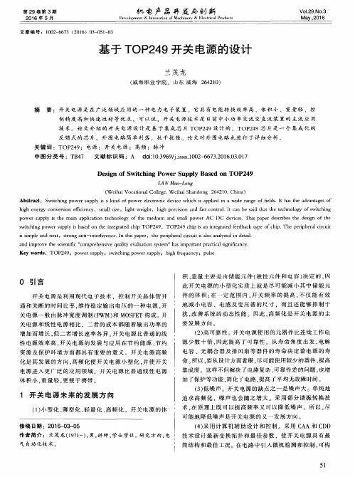
一、利用了TOP242N设计了一个实用的三路输出的开关电源,其输出分别为5V/0.6A、5V/0.1A、15V/0.15A,电路原理图如图1所示。
要求输入电压范围为交流80~400V,输出总功率约为6W左右。
1)前端电路设计当输入电压要求为AC400V时,考虑输入时电源的波动变化为±15%,则最高输入电压将达到460V左右,此输入电压经整流滤波后,其电压可达650V左右,再考虑加上输出反馈的电压Uor和漏感形成的尖峰电压叠加后其最高电压将超过800V,而该芯片的最高电压为700V,为了保证TOP242能正常安全工作,在设计前端电路时增加了一个MOS管,让MOS管与TOP242串接,并实现与TOP管同步开关来提高整体耐压。
本设计采用的MOS管是IR公司的IRFBC20,其耐压为600V,导通关断时间为几十个ns,这可以大大减少开关损耗。
MOS管的通断由TOP242N 控制,这样可以使MOS管和TOP242N内部的开关管时序保持一致,见图1。
2)外围控制电路设计该电路将TOP242N的极限电流设置为内部最大值,将TOP242N设为全频工作方式,开关频率为132kHz,把多功能脚M与S短接。
- 1、下载文档前请自行甄别文档内容的完整性,平台不提供额外的编辑、内容补充、找答案等附加服务。
- 2、"仅部分预览"的文档,不可在线预览部分如存在完整性等问题,可反馈申请退款(可完整预览的文档不适用该条件!)。
- 3、如文档侵犯您的权益,请联系客服反馈,我们会尽快为您处理(人工客服工作时间:9:00-18:30)。
TOP246-TOP249系列单片开关电源应用1.高效率70W通用开关电源模块TOPSwitch GX适合制作低成本、高效率、小尺寸、全密封式开关电源模块或电源适配器(adapter)。
由TOP249Y构成的密封式70W(19V,3.6A)通用开关电源模块,电路如图1所示。
当环境温度不超过40℃时,模块的外形尺寸可减小到10.5mm×5.5mm×2.5mm。
设计的交流输入电压范围是85V~265V,这属于全世界通用的电压范围。
该电源能同时实现输入欠压保护、过压保护、从外部设定极限电流、降低最大占空比等功能,其主要技术指标为:额定输出功率PO=70W;负载调整率SI=±4%;电源效率η≥84%(当交流输入电压U=85V时,满载效率可达85%;当U=230V时,电源效率高达90%);空载功率损耗<0.52W(U=230V时);图1高效率70W通用开关电源模块电路输出纹波电压≤120mV(峰峰值)。
该电源共使用3片集成电路:TOP249Y型6端单片开关电源(IC1);线性光耦合器PC817A(IC2);可调式精密并联稳压器TL431(IC3)。
电阻R9和R10用来从外部设定功率开关管的漏极极限电流,使之略高于满载或输入欠压时的漏极峰值电流ID(PK)。
这就允许在电源起动过程中或输出负载不稳定但未出现饱和的情况下,采用较小尺寸的高频变压器。
当输入直流电压过压时。
R9和R10还能自动降低最大占空比DMAx,对最大负载功率加以限制。
R11为欠压或过压检测电阻,并能给线路提供电压前馈,以减少开关频率的波动。
取R11=2MΩ时,仅当直流输入UI电压达到100V时,电源才能起动。
TOPSwitchGX的欠压电流IUV=50μA,过压电流IOV=225μA。
有公式UUV=IUV·R11(1)UOV=IOV·R11(2)将R11=2MΩ分别代入式(1)和式(2)中得到,UUV=100V(DC),UOV=450V (DC)。
过压时最大占空比DMAx随流入X端的电流IX的增大而减小,当IX从90μA增加到190μA时,最大占空比DMAx就从78%(对应于UUV=100V)线性地降低到47%(对应于375V)。
在掉电后,欠压检测能在C1放电时减少输出干扰,只要出现输出调节失效或者输入电压低于40V的情况,都会使TOPSwitch GX关闭。
当开关电源受到450V 以上的冲击电压时,R11同样可使TOP249关断,避免元器件受到损坏。
由VDZ1和VD1构成的漏极钳位电路,能吸收在MOSFET关断时由高频变压器初级漏感产生的尖峰电压,保护MOSFET不受损坏。
VDZ1采用钳位电压为200V的P6KE200型瞬态电压抑制器,VD1选用UF4006型超快恢复二极管,其反向耐压为800V。
将电容C11和VDZ1并联后,能减少钳位损耗。
选择全频工作方式时,开关频率设定为132kHz。
为了减小次级绕组和输出整流管的损耗,现将次级绕组分成两路,每路单独使用一只MBR20100型20A/100V的共阴极肖特基对管(VD2、VD3),然后并联工作。
输出滤波电路由C2、C3、L1、C4和C14构成。
空载时,TOP249Y能自动降低开关频率,使得在交流230V输入时电源损耗仅为520mW。
TOP249Y具有频率抖动特性,这对降低电磁干扰很有帮助。
只要合理地选择安全电容C7和EMI滤波器(L2、L3、C6)的元件值,就能使开关电源产生的电磁辐射符合CISPR22(FCCB)/EN55022B国际标准。
将C7的一端接UI的正极,能把TOP249Y的共模干扰减至最小。
需要指出,C7和C6都称作安全电容,区别只是C7接在高压与地之间,能滤除初、次级耦合电容产生的共模干扰,在IEC950国际标准中称之为“Y电容”。
C6则接在交流电源进线端,专门滤除电网线之间的差模干扰,被称作“X电容”。
精密光耦反馈电路由IC2、IC3等组成。
输出电压UO通过电阻分压器R4~R6获得取样电压,与TL431中的2.50V基准电压进行比较后产生误差电压,再经过光耦去改变TOP249Y的控制端电流IC,使占空比发生变化,进而调节UO保持不变。
反馈绕组的输出电压经VD4、C15整流滤波后,给光耦中的接收管提供偏压。
C5还与R8一起构成尖峰电压滤波器,使偏置电压在负载较重时能保持恒定。
R7、C9、C10和R3、C5、C8均为控制环路的补偿元件。
2由TOP249Y构成的DC/DC变换式250W开关电源该DC/DC变换式开关电源采用一片TOP249Y,输入为250V~380V直流电压,输出为48V、5.2A(250W),电源效率可达84%。
其电路如图2所示。
C1为高频滤波电容,专门抑制从输入端引入的电磁干扰。
由于TOP249工作在它的功率上限,因此需将X端与源极S短接,把极限电流设置为内部最大值,即ILIMIT=ILIMIT(max)=5.7A。
在L端到UI之间接一只2MΩ的电阻R1,可进行线路检测。
若UI>450V,则TOP249Y停止工作,直到电压恢复正常。
这就有效地防止了元器件损坏。
由于初级电流较大,须采取以下措施:第一,采用低泄漏电感的高频变压器并在初、次级之间增加屏蔽层,将漏感减至最小;第二,在钳位保护电路中的瞬态电压抑制器两端并联阻容元件R2、R3、C6,构成保护功能完善的VDZ1、VD1、R、C型钳位及吸收电路,以便吸收掉漏感上较大的磁场能量。
这种设计的优点在于,正常工作时VDZ1的损耗非常小,泄漏磁场能量主要由R2和R3分担;VDZ1的关键作用是限制在起动(或过载)情况下的尖峰电压,确保内部MOSFET的漏极电压低于700V。
次级绕组电压首先经过VD2、C9、C10和C11整流、滤波,再通过L2、C12滤除开关噪声之后,获得稳定的直流输出电压UO。
为减小滤波电容的等效电感,现将C9、C10和C11作并联使用。
稳压管VDZ2、VDZ3和VDZ4的稳压值分别为22V、12V、12V,串联后的总稳压值UZ=46V,稳定电流IZ≈10mA。
设光耦中红外发光二极管LED的正向压降为UF,输出电压由下式确定:图2-250W开关电源电路UO=UZ+UF+UR6≈46V+1V+10mA×100Ω=48VR6是LED的限流电阻,它还决定控制环路的增益。
二极管VD4和电容C14构成软起动电路。
刚上电时,由于C14两端压降不能突变,致使VD6因负极接低电平而导通,此时稳压管不工作。
随着C14被充电,其两端的压降不断升高,又使VD4变成截止状态,输出电压才建立起来。
掉电后,C14上的电荷就经过R9泄放掉。
C13和R8为高压控制回路的频率补偿元件。
为了保证TOP249Y能在满载情况下正常输出,必须给TOP249Y加上面积足够大的散热器,使芯片即使在低压输入或最高环境温度下工作,芯片的最高结温也不超过110℃(仅对Y封装而言,其他封装均不得超过100℃)。
若受安装条件限制,无法加装大散热器,则必须进行通风降温。
3由TOP246Y构成的45W多路输出式开关电源由TOP246Y构成45W多路输出式开关电源的电路如图3所示。
它可作为机顶盒、电报译码器、大容量硬盘驱动器或笔记本电脑的开关电源。
该电源在输入电压为交流185V~265V时,额定输出功率为45W,峰值输出功率可达60W;电源效率η≥75%,空载时的功耗仅为0.6W。
五路输出分别为:UO1(5V、3.2A)、UO2(3.3V、3A)、UO3(30V、0.03A)、UO4(18V、0.5A)、UO5(12V、0.6A);它们的负载调整率依次为±5%、±5%、±8%、±7%、±7%。
现将5V和3.3V作为主输出,并按一定的比例引入了反馈量,使这两路的稳压性能最佳。
其余各路为辅输出。
考虑到开关电源周围的环境温度较高,TOP246Y 适合给温度不超过60℃的标准机顶盒(SettopBox)供电,以利于降低传导损耗,减小散热器尺寸。
R2为极限电流设定电阻,取R2=9kΩ时,可将极限电流设定为典型值的80%,即=80%ILIMIT,从而限制了过载功率。
R1是线路检测电阻,当整流滤波后的直流输入电压超过450V时,它通过检测浪涌电流和瞬态电流来进行过压保护,迫使TOP246Y关断,起到了保护作用。
这对电网供电质量欠佳的地方尤为必要。
由VDZ1、VD6、R5和C5构成的初级钳位电路,能使漏极电压在所有情况下均低于700V。
R5和C5组成尖峰电压吸收电路,正常工作时可将瞬态电压抑制器VDZ1上的功率损耗降至最低,除非发生过载情况。
TOP246Y具有频率抖动特性,能有效抑制噪声干扰,因此只需在输入端加简单的EMI滤波器(C1,L1,C6)并采取合理的接地措施,即可符合有关电磁兼容性的CISPR2213国际标准。
刚上电时,利用热敏电阻(RT)可对C2的冲击电流加以限制,防止保险丝损坏。
压敏电阻(RV)的作用是吸收从电网窜入的浪涌电压。
为减小高频变压器的体积,次级绕组采用堆叠式绕法。
辅输出绕组的电位参考点接VD10的负极而不是正极,目的是把高压输出的电压偏差降至最小。
次级电压经过VD7~VD11、C7、C9、C11、C13、C16、C14和C17进行整流滤波。
VD11为3.3V输出电路中的整流管,选用MBR1045型10A/45V的肖特基二极管,肖特基二极管适于作低压、大电流整流,利用其低压降之特性,可提高电源效率。
VD10为5V输出的整流管,采用BYV32 200型20A/200V的超快恢复二极管。
3.3V和5V输出端的两只滤波电容需作并联使用,以减小输出端的纹波电流。
后置滤波器由L2~L5、C8′、C10、C12、C15和C18构成。
电阻R6可防止30V绕组端在轻载时的峰值充电电流。
3.3V输出经R11和R10取样后,接IC3(TL431A)的基准端,通过光耦IC2(LTV817)去调节TOP246Y的输出占空比。
R8为IC3提供偏置电流,R7用来设定整个反馈电路的直流增益。
R9、C19、R3和C5均为反馈电路中的补偿元件。
C20为软起动电容。
图3由TOP246Y构成的多路输出式45W开关电源电路4使用注意事项(1)输入滤波电容(图1、图2中为C1,图3中为C2)的负极应直接连反馈绕组(称之为开尔文连接),以便将反馈绕组上的浪涌电流直接返回到输入滤波电容,提高抑制浪涌干扰的能力。
(2)控制端附近的电容应尽可能靠近源极和控制端的引脚。
S极与C、L(或M)、X 极需各通过一条独立的支路相连,不得共享一条支路。
禁止让MOSFET的开关电流通过连接C S极的支路。
此外,S、L、X端的引线与外围相关元件的距离也要尽量短捷,并且远离漏极D的支路,以防止产生噪声耦合。