STA328 完美数字音频功放集成块
MP3内芯你懂吗

MP3内芯你懂吗?主流解码芯片详解MP3内芯你懂吗?主流解码芯片详解点击此处查看全部新闻图片如今购买MP3,理性的消费者一般不只关注外观以及功能,最主要还是机器本身的品质。
MP3的解码芯片已经为越来越多的消费者所关注,不过市场中几千款MP3,到底有哪些解码芯片为其提供良好的品质呢?那就请关注以下这篇文章吧!一、飞利浦芯片产地:荷兰如果一定要评出目前市场上最好的MP3解码芯片的话,那么无疑就是飞利浦芯片了。
飞利浦家族的解码芯片在业界一直以其“功能全,音质好,价格高”而著称。
飞利浦的解码芯片一般都采用的是BGA封装工艺,而国内的这方面技术相当有限,此外,由于飞利浦的解码芯片需要搭配另外的控制芯片电路协同工作,所以产品成本较高。
所以采用飞利浦解码芯片的厂商往往都定位于中高价位,如MPIO和IRIVER这两家韩国的MP3专业厂商。
这两个品牌一个最主要的共同特点就是在产品中全面采用了飞利浦的解码芯片。
因此,他们的产品拥有很高的音质和品质,成为全球MP3爱好者追逐的对象。
1、飞利浦SAA775X系列(SAA7750/7751/7752/7753)飞利浦SAA775x芯片是目前市场上MP3播放器解码芯片组中功能最全(支持CD直录),效果最好的解码芯片之一。
该解码芯片的音质表现为:低音下沉较深、中音表现出色、而相比之下高音则显得一般。
MP3内芯你懂吗?主流解码芯片详解点击此处查看全部新闻图片因为SAA775x中内含DSP(Digital Signal Processing,数字信号处理)和32位ARM RISC处理器,所以能用超高集成度的单颗芯片,音频解码和语音编码等工作,并且可以加入SDMI(Secure Digital Music Initiative,安全式数字音乐)保护其中SAA7750内含DSP和32位ARM RISC处理器,信噪比为90dB。
该芯片兼容多段多档位EQ智能音效,支持以AD PC M格式保存语音记录、同步显示歌名和歌曲信息、Line-in直录,此外还支持USB 1。
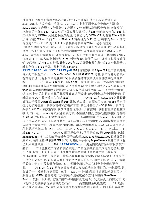
STA328中文资料

3 ORDERING INFORMATION
Figure 2. Block Diagram
SDA SCL
I2C System Contrlo
DDX-SPIRIT
LRCKI BICKI SDI_12
Serial Data Input, Channel
Mapping & Resampling
Audio EQ, Mix, Crossver,
OUT1A
Half Bridge
Half Bridge
OUT1B OUT2A
Channel 3
Half Bridge
OUT2B
3/41
STA328
Figure 8. Block Diagram (refer to Stereo Application Circuit)
VDD REG
19
VSS 35
Half Bridge
OUT1A
Half Bridge
Half Bridge
Half Bridge
OUT1B OUT2A
OUT2B
Figure 6. - 2.1-CCFG(1…0) = 01
Half Bridge
Half Bridge
Half Bridge
The STA328 power section consists of four independent half-bridges. These can be configured via digital control to operate in different modes. 2.1 channels can be provided by two half-bridges and a single full-bridge, providing up to 2x40W + 1x80W of power output. 2 Channels can be provided by two full-bridges, providing up to 2x80W of power. The IC can also be configured as a single paralelled full-bridge capable of high-current operation and 1x160W output.
功放芯片推荐

功放芯片推荐
功放芯片是一种广泛应用于音频放大器中的集成电路,主要用于放大输入信号,并将其输出到音箱或喇叭等输出设备。
在市场上,有许多不同类型的功放芯片可供选择,每种芯片都具有不同的特点和应用领域。
在这篇文章中,我将向您推荐几种常用的功放芯片,以供参考。
1. TDA7498E:这是一款非常受欢迎的功放芯片,具有高性能
和低功耗的特点。
它采用了双音频频道设计,能够输出较高功率的音频信号。
该芯片适用于汽车音频系统、家庭影音设备等多种应用场景。
2. TPA3116:这是一款数字功放芯片,采用了高效的BTL架构,能够实现低功耗和高保真度的音频放大。
它支持多种输入接口,包括模拟输入和数字输入,适用于音箱、耳机放大器等设备。
3. STA520:这是一款低功耗、高质量的功放芯片,适用于蓝
牙音箱等低功耗设备。
它具有低静态功率消耗、高动态范围和低噪声等特点,适合于要求高保真度的音频系统。
4. LM386:这是一款常用的单声道功放芯片,适用于便携式设备和小功率音箱。
它具有简单的电路结构和较高的增益,适合于电池供电的设备。
5. MAX9744:这是一款数字音频功放芯片,具有高效率和低
失真的特点。
它支持多种输入接口,包括模拟输入和数字输入,
适用于音箱、蓝牙音箱等设备。
以上仅是一些常见的功放芯片推荐,每一款芯片都有其适用的应用领域和特点,选择合适的芯片需要根据具体的应用需求来决定。
同时,还需要考虑功放芯片的品牌声誉、价格以及生产厂商的售后服务等因素,在选购之前需要综合考虑。
希望以上推荐能对您有所帮助。
四典型DA转换DAC0832芯片
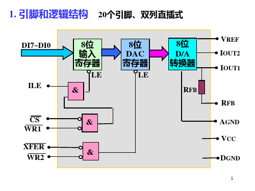
PC总线
DAC0832
D0 数 据 线 ~ D7
D~I0 DI7
RFB IOUT1
-
+5V
ILE IOUT2
+
Vo
IOW
A0 ~ A9
地址 译码
port
WR1 CS
XFER WR2
单缓冲工作方式 : 输入寄存器工作于受控状态 DAC寄存器工作于直通状态
9
D7~D0
+5V IOW
A9~A0
地址 译码
RFB
VREF IOUT2 IOUT1
RFB AGND VCC DGND
IOUT1
模拟电流输出端1 当输入数字为全”1”时, 输出电流最大,约为: 255VREF
256RFB 全”0”时, 输出电流为0
IOUT2 模拟电流输出端2 IOUT1 + I OUT2 = 常数
6
2. DAC0832与微机系统的连接 1)单缓冲工作方式
ILE
CS WR1 XFER WR2
8位 输入 寄存器
LE &
&
&
8位 DAC 寄存器
LE
8位 D/A 转换器
RFB
VREF IOUT2 IOUT1
RFB AGND VCC DGND
DI7~ DI0 数字量输入信号 其中: DI0为最低位,DI7为最高位
3
DI7~DI0
ILE
CS WR1 XFER WR2
一、A/D 转换器的基本原理(自学) 二、A/D转换器的技术指标(自学) 三、A/D转换器及其连接 四、典型A/D转换器
23
一、A/D 转换器的基本原理(自学) 数字输出量 A/D转换器 模拟输入量
TDA2822电路图详解

TDA2822详解,(后附电路图)一般的集成功放电路外围元件较多且需要较大的散热器。
本文介绍的功放电路简单,自制方便。
TDA2822集成功放电路常用在随身听、便携式的DVD等音频放音用;功率不是很大但以可以满足您的听觉要求了,且有电路简单、音质好、电压范围宽等特点,是业余制作小功放的较佳选择。
制造商: STMicroelectronicsTDA2822产品种类: 音频功率放大器(Audio Power Amplifier)产品类型: Class-AB(AB类音频功率放大器)输出功率: 1.7W输出类型: 1-Channel Mono or 2-Channel Stereo(桥接单声道或立体声双声道)可用增益调整: 39 dB总谐波失真+噪声(THD+N): 0.2 % @ 8 Ohm(Ω) @ 500 mW电源电压(最大值): 15 V电源电压(最小值): 1.8 V电源类型: Single(单电源)电源电流: 12 mA最大功率耗散: 4000 mW最小工作温度: - 40°C最大工作温度: 85°C封装/箱体: PDIP-16封装: Tube音频负载电阻: 8 Ohm(Ω)输入偏流(最大值): 0.1 μA (Type,典型值) @ 6V输入信号类型: Single输出信号类型: Differential or Single集成电路TDA2822M为8脚双列直插式封装,如果买不到可用TDA2822代替,TDA2822TDA2822的封装与TDA2822M相同,它们区别在于:TDA2822M从3V到15V 均可工作,而TDA2822的最高工作电压只有8V。
使用TDA2822必须把电压降到8V以下。
R1的数值要求不拘,一般选用10k的碳膜电阻。
C1可选用0.1uF的涤纶电容,C2为100uF/16V的电解电容。
使用时应注意:由于本功放为直接耦合,所以输入信号不能带直流成分。
如果输入信号有直流成分则必须在输入端串接一只4.7-10uF左右的电容隔开,否则将有很大的直流电流流过扬声器,使之发热烧毁。
音频处理芯片AIC23完整中文资料

⾳频处理芯⽚AIC23完整中⽂资料TLV320AIC23中⽂资料管脚图及其应⽤TLV320AIC23(以下简称AIC23)是TI推出的⼀款⾼性能的⽴体声⾳频Codec芯⽚,内置⽿机输出放⼤器,⽀持MIC和LINE IN两种输⼊⽅式(⼆选⼀),且对输⼊和输出都具有可编程增益调节。
AIC23的模数转换(ADCs)和数模转换(DACs)部件⾼度集成在芯⽚内部,采⽤了先进的Sigma-delta过采样技术,可以在8K到96K的频率范围内提供16bit、20bit、24bit和32bit的采样,ADC和DAC的输出信噪⽐分别可以达到90dB 和100dB。
与此同时,AIC23还具有很低的能耗,回放模式下功率仅为23mW,省电模式下更是⼩于15uW。
由于具有上述优点,使得AIC23是⼀款⾮常理想的⾳频模拟I/O器件,可以很好的应⽤在随声听(如CD,MP3……)、录⾳机等数字⾳频领域。
AIC23的管脚和内部结构框图如下:从上图可以看出,AIC23主要的外围接⼝分为以下⼏个部分:⼀.数字⾳频接⼝:主要管脚为BCLK-数字⾳频接⼝时钟信号(bit时钟),当AIC23为从模式时(通常情况),该时钟由DSP产⽣;AIC23为主模式时,该时钟由AIC23产⽣;LRCIN-数字⾳频接⼝DAC⽅向的帧信号(I2S模式下word时钟)LRCOUT-数字⾳频接⼝ADC⽅向的帧信号DIN-数字⾳频接⼝DAC⽅向的数据输⼊DOUT-数字⾳频接⼝ADC⽅向的数据输出这部分可以和DSP的McBSP(Multi-channel buffered serial port,多通道缓存串⼝)⽆缝连接,唯⼀要注意的地⽅是McBSP 的接收时钟和AIC23的BCLK都由McBSP的发送时钟提供,连接⽰意图如下:⼆.麦克风输⼊接⼝:主要管脚为MICBIAS-提供麦克风偏压,通常是3/4 AVDDMICIN-麦克风输⼊,由AIC结构框图可以看出放⼤器默认是5倍增益连接⽰意图如下:三.LINE IN输⼊接⼝:主要管脚为LLINEIN-左声道LINE IN输⼊RLINEIN-右声道LINE IN输⼊连接⽰意图如下:四.⽿机输出接⼝:主要管脚为LHPOUT-左声道⽿机放⼤输出RHPOUT-右声道⽿机放⼤输出LOUT-左声道输出ROUT-右声道输出从框图可以看出,LOUT和ROUT没有经过内部放⼤器,所以设计中常⽤LHPOUT和RHPOUT,连接⽰意图如下:五.配置接⼝:主要管脚为SDIN-配置数据输⼊SCLK-配置时钟DSP通过该部分配置AIC23的内部寄存器,每个word的前7bit为寄存器地址,后9bit 为寄存器内容。
主流功放芯片介绍

主流功放芯片介绍主流功放芯片是指当前市场上应用广泛的功率放大器芯片。
功率放大器(Power Amplifier,PA)是一种将输入信号的功率放大到更高功率的电子设备,用于驱动扬声器、放大音频信号或射频信号等功率放大应用。
下面将介绍几种主流的功放芯片。
1.TDA2030TDA2030是一种具有双向直流功率电源的5引脚单片电容器直接连接立体声功放器。
它采用了固定的直流偏置和电源电压补偿,具有较低的失真和幅频特性,使其成为一种广泛应用于音频放大领域的主流功放芯片之一、TDA2030适用于低音频放大应用,如音乐播放器、家庭影院系统等。
2.TDA7294TDA7294是一种高性能音频功放芯片,具有单声道输出功率100W和双声道输出功率50W。
它采用了多功能内部保护电路,具有过温保护、过电流保护和短路保护等功能,可以保证功放的稳定工作。
TDA7294还具有低高频失真和低噪声等优点,适用于高品质音频放大应用,如音响系统、专业音箱等。
3.LM3886LM3886是一种高性能音频功放芯片,具有单声道输出功率68W。
它采用了内部限流和短路保护电路,可以保护功放芯片免受损坏。
LM3886还具有低失真、低噪声和高稳定性等特点,适用于高保真音响系统、音乐工作室等高要求音频放大应用。
4.TPA3116TPA3116是一种数字音频功放芯片,具有高效率、低功耗和高音质的特点。
它采用了数字输入和PWM调制技术,可以实现高保真的音频放大。
TPA3116还具有多种保护功能,如过温保护、过电流保护和低电压保护等,可以保护功放芯片的安全工作。
TPA3116适用于便携式音箱、无线音乐播放器等功率放大应用。
以上介绍了几种主流的功放芯片,它们在不同的应用领域中具有各自的特点和优势。
用户可以根据自己的需求选择合适的功放芯片来实现音频信号的放大。
目前市面上流行的音频处理芯片汇总
目前市面上流行的音频处理芯片汇总一下,目前我们使用的较为熟练的为ADAU1701,与大家分享. 美国Cirrus Logic上市了用于车载音响放大器,集32bit DSP、4声道A-D转换器、8声道A-D转换器以及数码音响接口(收发信)电路等于一身的SoC“CS47048”(英文发布资料).以DSP性能高为特点. DSP的工作频率为150MHz.为固定小数点类型,运算能力为300MMACS.配备有72bit的累加器.内置32K word的32bit SRAM.A-D转换器为ΔΣ型,分辨率为24bit.动态范围为105dB,THD+N为98dB.D-A转换器分辨率为24bit,动态范围为108dB,THD+N为98dB.输入、输出信号均支持单端信号和差分信号.数码音响接口电路支持S/PDIF、TDM及I2S各种规格的收发.采样频率最大为192kHz,支持32bit分辨率的音频数据.备有支持SPI、I2C的控制用串行接口. 电源电压方面,内核为+1.8V,输入输出电路为+3.3V.封装为100端子的LQFP.备有工作温度范围0~+70℃和-40~+85℃的型号.计划2008年12月开始样品供货.每1万个批量购入时的单价为6.12美元. 资料下载 cs470781227429840.pdf1227429887.pdf ADI日前宣布,其SigmaDSP数字音频处理器系列三款新产品──ADAV400、ADAU1701和ADAU1702问世,新产品针对音频系统等需求设计,包括高清电视(HDTV)以及多媒体播放器使用的便携式扬声器系统. ADI表示,ADAV400具备125MHz的速度,符合新一代高清平面电视(如LCD电视)对音频处理的需求.该产品整合56位音频处理核心,以及具有超过95dB动态范围的模拟数字转换器(ADC)和数字模拟转换器(DAC).并包含一组延迟内存,针对弥补目前电视的视频处理延迟所设计,能使影像与声音同步传送,同时还支持16个数字输出入信道(I2S). ADAU1701和ADAU1702则使设计者可选择采用50MHz或25MHz的DSP引擎,适合数字音频应用方案,如MP3随身听使用的扩充基座、车载收音机和接电扩音器.新组件整合了ADC和DAC、多信道数字I/O(I2S)与延迟内存,以及具备自行开机、外部控制、实体按键和音量控制接口,为一组turnkey系统设计解决方案,不需额外的处理器或微控制器,适合搭配ADIAD199x Class-D放大器系列. 新组件并可与SigmaStudio GUI(图形使用者界面)设计工具合并使用;该工具拥有易于使用的拖曳画面,数据库内的区块包括音量控制、跨接及等化滤波器、动态处理器等.SigmaStudio并支持多种业界标准算法,如SRS TruSurroundXT、Waves MaxxBass、Dolby Prologic-II 或BBE-Viva. ADAV400现正提供样本,采用无铅80脚LQFP封装,包括SigmaStudio设计工具的评估板也已开始供货.ADAU1701和ADAU1702目前开始供应样本,采用无铅48接脚LQFP封装,两者的评估板与SigmaStudio设计工具同样已开始限量供应. adau1701 1227430054.pdf满足消费类音频对高保真度的要求为了强化致力为消费类音频电子产品提供高质量集成电路的决心,德州仪器|仪表 (TI) 日前宣布其高性能数字音频处理器系列又添一款新成员.TAS3308 音频片上系统是一款单芯片SoC 解决方案,为音响设备制造商提供了出色的处理性能,以创建各种可满足严格要求的应用,如数字电视 (DTV) 音频子系统、迷你∕微型组合音响、5.1 条形音箱以及其它消费类音频电子产品. TAS3308 在TI 原有高端音频解决方案的基础上得到了进一步增强,其集成了一个模拟多路复用器、立体声 ADC、一个高性能数字音频处理器以及六个脉宽调制 (PWM) 输出通道.这种高硬件集成度配合直观易用的 PurePath Studio 软件开发环境,使客户能在尽可能降低软硬件开发资源投入的情况下,向市场推出高级数字音频信号处理产品. 高性能的系统级集成TI 最新处理器采用包括 PWM 输出在内的全面集成数字音频信号链,有助于降低系统成本与复杂性,并允许直接驱动 D 类功率级.这款 TAS3308 音频 SoC 建立在 TI 大获成功的音频处理器系列所采用的业经验证的技术基础之上,这个技术已被领先制造商的一系列消费类音频产品采用.新器件的核心组件是基于业界领先的TI 数字信号处理技术的高性能数字音频处理器.出色的高分辨率音频处理技术要归功于 48 位数据路径,该路径提供了高级音频算法所需的高精度处理能力.135 MHz 运行速度的 TAS3308 处理器还包含一个可进行控制与通信的片上微控制器,从而优化了系统性能.集成的模拟功能包含一个 100 dB 动态范围(DNR) 的立体声单端 ADC、一个十输入通道的模拟多路复用器,以及六个 105 dB DNR 的差动 PWM 输出. 该器件的处理性能优势可帮助设计人员实现高清电视等产品的性能增值,以满足消费者对高保真音质的要求,切实与高清画面匹配.更多详情,敬请访问:/tas3308. TI 混合信号音频与视频产品部的产品线经理 Cecelia Smith 指出:“TI TAS3308 音频 SoC 为系统设计人员提供了各种简单易用的数字输出选择方案,可满足高清电视与其它高端音频消费类电子产品的设计要求.借助 TAS3308 与其它音频解决方案,TI 努力为设计人员提供所需的高性能、灵活性、低成本与技术支持,以帮助他们向消费类市场推出有竞争优势的增值产品.” 有助于节省时间的开发支持针对TAS3308 的灵活深入的软件支持有助于加速产品上市进程,提高定制化与产品差异化水平,能够帮助开发人员以更低成本为消费者提供高质量音频.该器件得到了传统 DSP 软件开发五金|工具套件与 PurePath Studio 图形开发环境的全面支持,这种高效拖放开发环境能够加速新音频产品的设计工作.开发人员能全面控制音频处理过程,并充分利用 TI 与主要第三方合作伙伴推出的丰富的预编程基本音频功能与高级音频算法系列. 适合完整解决方案的 PWM 放大器 TAS3308 SoC 与 TI PWM 功率级的 TAS5xxx 系列可以互相补充.TAS3308 的PWM 控制与 TAS5xxx 功率级在设计时采用 TI 业经市场验证的 PurePath PWM 技术,实现了板级无缝协作,确保了简便的系统集成与高质量的音频性能,并尽可能减少了开发工作.TAS5xxx 器件实现了引脚兼容与电源|稳压器可扩展 (power-scalable),这样,音频设计人员能够在 TAS3308 板面布局基本不变的基础上,创建多种多信道系统配置,实现 13 W 至 315 W 的单位通道输出范围. TAS3308 片上音频系统现已开始提供样片,计划于 2008 年第一季度开始批量供货.该器件采用 100 引脚 QFP 封装. TI 致力提供更丰富的家庭娱乐音频产品 TAS3308 是 TI 针对家庭娱乐音频的完整产品系列的组成部分.从业界领先的 DSP 到高性能仿真产品 (HPA) 解决方案,TI 为简单与复杂的音频设计提供了最高可靠性、最大可扩展性的低功耗解决方案. tas3308资料1227430190.pdf。
- 1、下载文档前请自行甄别文档内容的完整性,平台不提供额外的编辑、内容补充、找答案等附加服务。
- 2、"仅部分预览"的文档,不可在线预览部分如存在完整性等问题,可反馈申请退款(可完整预览的文档不适用该条件!)。
- 3、如文档侵犯您的权益,请联系客服反馈,我们会尽快为您处理(人工客服工作时间:9:00-18:30)。
May 2008 Rev 41/57STA3282.1-channel high-efficiency digital audio systemFeatures!Wide supply voltage range (10 V - 36V)!Three power output configurations –2x 40W + 1x 80W –2x 80W –1x 160W !PowerSO-36 package ! 2.1 channels of 24-bit DDX ®!100-dB SNR and dynamic range !32kHz to 192kHz input sample rates !Digital gain/attenuation +48dB to -80dB in 0.5-dB steps!Four 28-bit user programmable biquads (EQ) per channel !I 2C control!2-channel I 2S input data interface!Individual channel and master gain/attenuation !Individual channel and master soft/hard mute !Individual channel volume and EQ bypass !Bass/treble tone control!Dual independent programmable limiters/compressors!AutoModes–32 preset EQ curves–15 preset crossover settings –Auto volume controlled loudness – 3 preset volume curves– 2 preset anti-clipping modes –Preset night-time listening mode –Preset TV AGC!Input and output channel mapping !AM noise-reduction and PWM frequency-shifting modes!Software volume update and muting !Auto zero detect and invalid input detect muting!Selectable DDX ® ternary or binary PWM output + variable PWM speeds !Selectable de-emphasis!Post-EQ user programmable mix with default 2.1 bass-management settings!Variable max power correction for lower full-power THD!Four output routing configurations !Selectable clock input ratio!96kHz internal processing sample rate, 24 to 28-bit precision!Video application supports 576 * fs input mode.Table 1.Device summaryOrder codePackagePackagingST A328PowerSO-36Tube ST A32813TRPowerSO-36Tape and reelContents STA328Contents1Description . . . . . . . . . . . . . . . . . . . . . . . . . . . . . . . . . . . . . . . . . . . . . . . . . 51.1Overview . . . . . . . . . . . . . . . . . . . . . . . . . . . . . . . . . . . . . . . . . . . . . . . . . . 51.2EQ processing . . . . . . . . . . . . . . . . . . . . . . . . . . . . . . . . . . . . . . . . . . . . . . 61.3Output configurations . . . . . . . . . . . . . . . . . . . . . . . . . . . . . . . . . . . . . . . . . 61.4Applications . . . . . . . . . . . . . . . . . . . . . . . . . . . . . . . . . . . . . . . . . . . . . . . . 72Pin out . . . . . . . . . . . . . . . . . . . . . . . . . . . . . . . . . . . . . . . . . . . . . . . . . . . . 82.1Package pins . . . . . . . . . . . . . . . . . . . . . . . . . . . . . . . . . . . . . . . . . . . . . . . 82.2Pin list . . . . . . . . . . . . . . . . . . . . . . . . . . . . . . . . . . . . . . . . . . . . . . . . . . . . . 82.3Pin description . . . . . . . . . . . . . . . . . . . . . . . . . . . . . . . . . . . . . . . . . . . . . . 93Electrical specifications . . . . . . . . . . . . . . . . . . . . . . . . . . . . . . . . . . . . . 113.1General interface specifications . . . . . . . . . . . . . . . . . . . . . . . . . . . . . . . . 113.2DC electrical specifications (3.3V buffers) . . . . . . . . . . . . . . . . . . . . . . . . 123.3Power electrical specifications . . . . . . . . . . . . . . . . . . . . . . . . . . . . . . . . . 12 4Electrical characteristics curves . . . . . . . . . . . . . . . . . . . . . . . . . . . . . . 145I2C bus specification . . . . . . . . . . . . . . . . . . . . . . . . . . . . . . . . . . . . . . . . 165.1Communication protocol . . . . . . . . . . . . . . . . . . . . . . . . . . . . . . . . . . . . . . 165.2Device addressing . . . . . . . . . . . . . . . . . . . . . . . . . . . . . . . . . . . . . . . . . . 165.3Write operation . . . . . . . . . . . . . . . . . . . . . . . . . . . . . . . . . . . . . . . . . . . . . 175.4Read operation . . . . . . . . . . . . . . . . . . . . . . . . . . . . . . . . . . . . . . . . . . . . . 176Register description . . . . . . . . . . . . . . . . . . . . . . . . . . . . . . . . . . . . . . . . 196.1Configuration register A (addr 0x00) . . . . . . . . . . . . . . . . . . . . . . . . . . . . 206.2Configuration register B (addr 0x01) . . . . . . . . . . . . . . . . . . . . . . . . . . . . 236.3Configuration register C (addr 0x02) . . . . . . . . . . . . . . . . . . . . . . . . . . . . 266.3.1DDX® power output mode . . . . . . . . . . . . . . . . . . . . . . . . . . . . . . . . . . . 266.3.2DDX® variable compensating pulse size . . . . . . . . . . . . . . . . . . . . . . . . 266.4Configuration register D (addr 0x03) . . . . . . . . . . . . . . . . . . . . . . . . . . . . 276.5Configuration register E (addr 0x04) . . . . . . . . . . . . . . . . . . . . . . . . . . . . 29 2/57STA328Contents6.6Configuration register F (addr 0x05) . . . . . . . . . . . . . . . . . . . . . . . . . . . . 316.7Volume control . . . . . . . . . . . . . . . . . . . . . . . . . . . . . . . . . . . . . . . . . . . . . 336.7.1Master controls . . . . . . . . . . . . . . . . . . . . . . . . . . . . . . . . . . . . . . . . . . . 336.7.2Channel controls . . . . . . . . . . . . . . . . . . . . . . . . . . . . . . . . . . . . . . . . . . 336.7.3Volume description . . . . . . . . . . . . . . . . . . . . . . . . . . . . . . . . . . . . . . . . 336.8AutoMode registers . . . . . . . . . . . . . . . . . . . . . . . . . . . . . . . . . . . . . . . . . 356.8.1AutoModes EQ, volume, GC (addr 0x0B) . . . . . . . . . . . . . . . . . . . . . . . 356.8.2AutoMode AM/pre-scale/bass management scale (addr 0x0C) . . . . . . 366.8.3Preset EQ settings (addr 0x0D) . . . . . . . . . . . . . . . . . . . . . . . . . . . . . . . 376.9Channel configuration registers . . . . . . . . . . . . . . . . . . . . . . . . . . . . . . . . 386.9.1Channel 1 configuration (addr 0x0E) . . . . . . . . . . . . . . . . . . . . . . . . . . . 386.9.2Channel 2 configuration (addr 0x0F) . . . . . . . . . . . . . . . . . . . . . . . . . . . 386.9.3Channel 3 configuration (addr 0x10) . . . . . . . . . . . . . . . . . . . . . . . . . . . 386.10Tone control (addr 0x11) . . . . . . . . . . . . . . . . . . . . . . . . . . . . . . . . . . . . . 406.11Dynamics control . . . . . . . . . . . . . . . . . . . . . . . . . . . . . . . . . . . . . . . . . . . 416.11.1Limiter 1 attack/release threshold (addr 0x12) . . . . . . . . . . . . . . . . . . . . 416.11.2Limiter 1 attack/release threshold (addr 0x13) . . . . . . . . . . . . . . . . . . . . 416.11.3Limiter 2 attack/release rate (addr 0x14) . . . . . . . . . . . . . . . . . . . . . . . . 416.11.4Limiter 2 attack/release threshold (addr 0x15) . . . . . . . . . . . . . . . . . . . . 416.11.5Dynamics control description . . . . . . . . . . . . . . . . . . . . . . . . . . . . . . . . . 416.11.6Anti-clipping mode . . . . . . . . . . . . . . . . . . . . . . . . . . . . . . . . . . . . . . . . . 436.11.7Dynamic range compression mode . . . . . . . . . . . . . . . . . . . . . . . . . . . . 447User programmable processing . . . . . . . . . . . . . . . . . . . . . . . . . . . . . . 457.1EQ - biquad equation . . . . . . . . . . . . . . . . . . . . . . . . . . . . . . . . . . . . . . . . 457.2Pre-scale . . . . . . . . . . . . . . . . . . . . . . . . . . . . . . . . . . . . . . . . . . . . . . . . . 457.3Post-scale . . . . . . . . . . . . . . . . . . . . . . . . . . . . . . . . . . . . . . . . . . . . . . . . . 457.4Mix/bass management . . . . . . . . . . . . . . . . . . . . . . . . . . . . . . . . . . . . . . . 467.5Calculating 24-bit signed fractional numbers from a dB value . . . . . . . . . 477.6User defined coefficient RAM . . . . . . . . . . . . . . . . . . . . . . . . . . . . . . . . . . 477.6.1Coefficient address register 1 (addr 0x16) . . . . . . . . . . . . . . . . . . . . . . . 477.6.2Coefficient b1data register bits 23:16 (addr 0x17) . . . . . . . . . . . . . . . . . 477.6.3Coefficient b1data register bits 15:8 (addr 0x18) . . . . . . . . . . . . . . . . . . 477.6.4Coefficient b1data register bits 7:0 (addr 0x19) . . . . . . . . . . . . . . . . . . . 477.6.5Coefficient b2 data register bits 23:16 (addr 0x1A) . . . . . . . . . . . . . . . . 477.6.6Coefficient b2 data register bits 15:8 (addr 0x1B) . . . . . . . . . . . . . . . . . 483/57Contents STA3284/577.6.7Coefficient b2 data register bits 7:0 (addr 0x1C) . . . . . . . . . . . . . . . . . . 487.6.8Coefficient a1 data register bits 23:16 (addr 0x1D) . . . . . . . . . . . . . . . . 487.6.9Coefficient a1 data register bits 15:8 (addr 0x1E) . . . . . . . . . . . . . . . . . 487.6.10Coefficient a1 data register bits 7:0 (addr 0x1F) . . . . . . . . . . . . . . . . . . 487.6.11Coefficient a2 data register bits 23:16 (addr 0x20) . . . . . . . . . . . . . . . . 487.6.12Coefficient a2 data register bits 15:8 (addr 0x21) . . . . . . . . . . . . . . . . . 487.6.13Coefficient a2 data register bits 7:0 (addr 0x22) . . . . . . . . . . . . . . . . . . 487.6.14Coefficient b0 data register bits 23:16 (addr 0x23) . . . . . . . . . . . . . . . . 497.6.15Coefficient b0 data register bits 15:8 (addr 0x24) . . . . . . . . . . . . . . . . . 497.6.16Coefficient b0 data register bits 7:0 (addr 0x25) . . . . . . . . . . . . . . . . . . 497.6.17Coefficient write control register (addr 0x26) . . . . . . . . . . . . . . . . . . . . . 49 7.7Reading a coefficient from RAM . . . . . . . . . . . . . . . . . . . . . . . . . . . . . . . . 50 7.8Reading a set of coefficients from RAM . . . . . . . . . . . . . . . . . . . . . . . . . . 50 7.9Writing a single coefficient to RAM . . . . . . . . . . . . . . . . . . . . . . . . . . . . . 50 7.10Writing a set of coefficients to RAM . . . . . . . . . . . . . . . . . . . . . . . . . . . . . 51 7.11Variable max power correction (addr 0x27, 0x28) . . . . . . . . . . . . . . . . . . 53 7.12Fault detect recovery (addr 0x2B, 0x2C) . . . . . . . . . . . . . . . . . . . . . . . . . 538Package mechanical data . . . . . . . . . . . . . . . . . . . . . . . . . . . . . . . . . . . . 54 9Revision history . . . . . . . . . . . . . . . . . . . . . . . . . . . . . . . . . . . . . . . . . . . 56STA328Description 1 Description1.1 OverviewThe STA328 comprises digital audio processing, digital amplifier control and DDX® poweroutput stage to create a high-power single-chip DDX® solution for high-quality,high-efficiency, all digital amplification.The STA328 power section consists of four independent half-bridges. These can beconfigured via digital control to operate in different modes. 2.1 channels can be provided bytwo half-bridges and a single full-bridge to give up to 2x40W plus 1x80 W of poweroutput. Two channels can be provided by two full-bridges to give up to 2x80W of power.The IC can also be configured as a single parallel full-bridge capable of high-currentoperation and 1x160W output.Also provided in the ST A328 is a full assortment of digital processing features. This includesup to four programmable 28-bit biquads (EQ) per channel and bass/treble tone control.AutoModes enable a time-to-market advantage by substantially reducing the amount ofsoftware development needed for certain functions. This includes auto volume loudness,preset volume curves, preset EQ settings. New advanced AM radio-interference reductionmodes.The serial audio data input interface accepts all possible formats, including the popular I2Sformat.Three channels of DDX® processing are provided. This high-quality conversion from PCMaudio to patented DDX® 3-state PWM switching provides over 100dB of SNR and dynamicrange.5/57Description STA3286/571.2 EQ processingTwo channels of input data (re-sampled if necessary) at 96kHz are provided to the EQprocessing block. In this block, up to four user-defined biquads can be applied to each of the two channels.Pre-scaling, DC-blocking, high-pass, de-emphasis, bass, and tone control filters can also be applied based on various configuration parameter settings.The entire EQ block can be bypassed for all channels simultaneously by setting the DSPB bit to 1. And the CxEQBP bits can be used to bypass the EQ function on a per channel basis. Figure 3 shows the internal signal flow through the EQ block.1.3 Output configurationsSTA328Description 1.4 Applications7/57Pin out STA3288/572 Pin out2.1 Package pinsFigure 6.Pin connections2.2 Pin listVCC_SIGNVSS VDD GND BICKI LRCKI SDI VDDA GNDA XTIPLL_FILTER RESERVEDSDA SCL RESET CONFIGVLVDD_REG SUB_GND N.C.OUT2B VCC2B N.C.GND2B GND2A VCC2A OUT2A OUT1B VCC1B GND1B GND1A N.C.VCC1A OUT1AGND_CLEAN GND_REG363534333231302928272625242322212019123456789101112131415161718Table 2.Pin listNumber TypeNameDescription1I/O SUB_GND Ground 2N.C.N.C.Not connected 3O OUT2B Output half bridge 2B 4I/O VCC2B Positive supply 5N.C.N.C.Not connected 6I/O GND2B Negative supply 7I/O GND2A Negative supply 8I/O VCC2A Positive supply 9O OUT2A Output half bridge 2A 10O OUT1B Output half bridge 1B 11I/O VCC1B Positive supply 12I/O GND1B Negative supply 13I/O.GND1A Negative supply 14N.C.N.C.Not connectedSTA328Pin out9/572.3 Pin descriptionOUT1A, 1B, 2A and 2B (pins 16, 10, 9 and 3)Output half bridge PWM outputs 1A, 1B, 2A and 2B provide the input signals to thespeakers.RESET (pin 22)Driving RESET low sets all outputs low and returns all register settings to their default (reset) values. The reset is asynchronous to the internal clock.15I/O VCC1A Positive supply 16O OUT1A Output half bridge 1A 17I/O GND_CLEAN Logical ground 18I/O GND_REG Substrate ground 19I/O VDD_REG Logic supply 20I/O VL Logic supply 21I CONFIG Logic levels 22I RESET Reset23I SCL I 2C serial clock 24I/O SDA I 2C serial data25-RESERVED This pin must be connected to GND 26I PLL_FILTER Connection to PLL filter 27I XTI PLL input clock 28I/O GNDA Analog ground29I/O VDDA Analog supply, nominally 3.3 V 30I SDI I 2S serial data channels 1 & 231I/O LRCKI I 2S left/right clock, 32I BICKI I 2S serial clock 33I/O GND Digital ground34I/O VDD Digital supply, nominally 3.3V 35I/O VSS 5V regulator referred to +V CC 36I/OVCC_SIGN5V regulator referred to groundTable 2.Pin listNumber TypeNameDescriptionPin out STA32810/57I2C signals (pins 23 and 24)The SDA (I2C Data) and SCL (I2C Clock) pins operate according to the I2C specification (Chapter5 on page16 gives more information). Fast-mode (400kB/s) I2C communication is supported.GNDA and VDDA (pins 28 and 29)This is the 3.3 V analog supply for the phase locked loop. It must be well decoupled and filtered for good noise immunity since the audio performance of the device depends upon the PLL circuit.CLK (pin 27)This is the master clock in used by the digital core. The master clock must be an integer multiple of the LR clock frequency. Typically, the master clock frequency is 12.288MHz (256*fs) for a 48kHz sample rate; it is the default setting at power-up. Care must be taken to provide the device with the nominal system clock frequency; over-clocking the device may result in anomalous operation, such as inability to communicate.FILTER_PLL (pin 26)This is the connection for external filter components for the PLL loop compensation. The schematic diagram in Figure5 on page7 shows the recommended circuit.BICKI (pin 32)The serial or bit clock input is for framing each data bit. The bit clock frequency is typically 64*fs using I2S serial format.SDI_12 (pin 30)This is the serial data input where PCM audio information enters the device. Six format choices are available including I2S, left or right justified, LSB or MSB first, with word widths of 16, 18, 20 and 24 bits.LRCKI (pin 31)The left/right clock input is for data word framing. The clock frequency is at the input sample rate, fs.11/573 Electrical specificationsTable 3.Absolute maximum ratingsTable 4.Thermal dataTable 5.Recommended operating conditions3.1 General interface specificationsOperating conditions V DD33 = 3.3V ±0.3V , T amb = 25°C unless otherwise specifiedSymbol ParameterValueUnit V DD33 3.3V I/O power supply (pins VDDA, VDD)-0.5 to 4V V i Voltage on input pins -0.5 to (V DD33+0.5)V V o Voltage on output pins -0.5 to (V DD33+0.5)V T stg Storage temperature-40 to +150°C T amb Ambient operating temperature-20 to +85°C V CC DC supply voltage (pins VCCnA, VCCnB)40V V MAXMaximum voltage on VL (pin 20)5.5VSymbol ParameterMinTypMax Unit R thj-case Thermal resistance junction to case (thermal pad) 2.5°C/W T j-SD Thermal shut-down junction temperature 150°C T WARN Thermal warning temperature 130°C T h-SDThermal shut-down hysteresis25°CSymbol ParameterValueUnit V DD33 I/O power supply3.0 to 3.6V T jOperating junction temperature-20 to +125°CTable 6.General interface electrical characteristicsSymbol ParameterTest Condition Min.Typ.Max.Unit I il Low level input no pull-up V i = 0V (1)1.The leakage currents are generally very small (< 1 nA). The values given here are the maximum valuesafter an electrostatic stress on the pin.1µA I ih High level input no pull-downV i = V DD33 (1)2µA I OZ 3-state output leakage withoutpull-up/downV i = V DD33 (1)2µA V esdElectrostatic protection (human-body model)Leakage current < 1µA2000V12/573.2 DC electrical specifications (3.3V buffers)Operating conditions V DD33 = 3.3V ±0.3V , T amb = 25°C unless otherwise specified3.3 Power electrical specificationsOperating conditions V DD33 = 3.3V ±0.3V , V L =3.3V , V CC =30V ,T amb = 25°C unless otherwise specified.Table 7.DC electrical specificationsSymbol ParameterTest conditionMin.Typ.Max.Unit V IL Low level input voltage 0.8V V IH High level input voltage 2.0V V hyst Schmitt trigger hysteresis 0.4V V ol Low level output IoI = 2mA 0.15V V ohHigh level outputIoh = -2mAV DD33- 0.15VTable 8.Power electrical characteristicsSymbol ParameterTest conditions Min.Typ.Max.Unit R dsON Power Pchannel/Nchannel MOSFET RdsON Id =1A 200270m Ω I dss Power Pchannel/Nchannel leakage IdssV CC = 35V 50µA g N Power Pchannel RdsON matchingId =1A 95%g P Power Nchannel RdsON matchingId =1A95%Dt_s Low current dead time (static)See test circuits, Figure 7 and Figure 81020ns t d ON Turn-on delay time Resistive load 100ns t d OFF Turn-off delay time Resistive load100ns t r Rise time Resistive load, Figure 7 and Figure 825ns t f Fall time Resistive load, Figure 7 and Figure 825ns V CC Supply voltage1036V V L Low logical state voltage VL V L = 3.3V 0.8V V H High logical state voltage VH V L = 3.3V 1.7V I VCC-PWRDNSupply current from V CC in PWRDNPin PWRDN = 0 V 3mA I VCC-hizSupply current from V CC in 3-stateV CC =30V , 3-state22mA13/57Figure 7.Test circuit 1I VCCSupply current from V CC in operation(both channel switching)Input pulse width = 50% duty,switchingfrequency =384kHz,no LC filters80mAI out-sh Overcurrent protectionthreshold (short circuit current limit)4.56AV UV Undervoltage protection threshold7V t pw-min Output minimum pulse width No load70150ns P oOutput power (refer to test circuitTHD = 10%R L = 4Ω, V CC = 21V R L = 8Ω, V CC = 36V 5080W W P oOutput power (refer to test circuitTHD = 1%R L = 4Ω, V CC = 21V R L = 8Ω, V CC = 36V4062W WTable 8.Power electrical characteristics (continued)SymbolParameterTest conditions Min.Typ.Max.UnitDT rDTfVcc (3/4)Vcc(1/2)Vcc (1/4)VcctOUTxYLow current dead time = MAX(DT r, DTf)+VccDuty cycle = 50%INxYM58M57OUTxYgndvdc = Vcc/2V67R 8W+-4 Electrical characteristics curves14/5715/57I 2C bus specificationSTA32816/575 I 2C bus specificationThe STA328 supports the I 2C protocol. This protocol defines any device that sends data on to the I 2C bus as a transmitter and any device that reads the data as a receiver. The device that controls the data transfer is known as the master and the other as the slave. The master always starts the transfer and provides the serial clock for synchronization. The STA328 is always a slave device in all of its communications.5.1 Communication protocolData transition or changeData changes on the SDA line must only occur when the SCL clock is low. SDA transitionwhile the clock is high is used to identify a START or STOP condition.Start conditionSTART is identified by a high to low transition of the data bus SDA signal while the clock signal SCL is stable in the high state. A START condition must precede any command for data transfer.Stop conditionSTOP is identified by a low to high transition of the data bus SDA signal while the clock signal SCL is stable in the high state. A STOP condition terminates communication between STA328 and the bus master.Data inputDuring the data input the STA328 samples the SDA signal on the rising edge of clock SCL. For correct device operation the SDA signal must be stable during the rising edge of the clock and the data can change only when the SCL line is low.5.2 Device addressingTo start communication between the master and the STA328, the master must initiate with astart condition. Following this, the master sends 8 bits (MSB first) onto the SDA line corresponding to the device select address and read or write mode.The 7 MSBs are the device address identifiers, corresponding to the I 2C bus definition. The STA328 device address is decimal 34 (binary 00100010).The 8th bit (LSB) identifies read or write operation, RW. This bit is set to 1 in read mode and 0 for write mode. After a START condition the STA328 identifies the device address on the bus. If a match is found, it acknowledges the identification on the SDA bus during the 9th bit time. The byte following the device identification byte is the internal space address.STA328I 2C bus specification17/575.3 Write operationFollowing the START condition the master sends a device select code with the RW bit setto 0. The ST A328 acknowledges this and then the master writes the internal address byte. After receiving the internal byte address the STA328 again responds with an acknowledgement.2Byte writeIn the byte write mode the master sends one data byte. This is acknowledged by the STA328. The master then terminates the transfer by generating a STOP condition.Multi-byte writeThe multi-byte write modes can start from any internal address. Sequential data byte writes will be written to sequential addresses within the STA328. The master generating a STOP condition terminates the transfer.5.4 Read operation2Current address byte readFollowing the START condition the master sends a device select code with the RW bit set to 1. The STA328 acknowledges this and then responds by sending one byte of data. The master then terminates the transfer by generating a STOP condition.I2C bus specification STA32818/57Current address multi-byte readThe multi-byte read modes can start from any internal address. Sequential data bytes will be read from sequential addresses within the STA328. The master acknowledges each data byte read and then generates a STOP condition terminating the transfer.Random address byte readFollowing the START condition the master sends a device select code with the RW bit set to0. The ST A328 acknowledges this and then the master writes the internal address byte. After receiving, the internal byte address the STA328 again responds with an acknowledgement. The master then initiates another ST ART condition and sends the device select code with the RW bit set to 1. The ST A328 acknowledges this and then responds by sending one byte of data. The master then terminates the transfer by generating a STOP condition.Random address multi-byte readThe multi-byte read modes could start from any internal address. Sequential data bytes will be read from sequential addresses within the ST A328. The master acknowledges each data byte read and then generates a STOP condition terminating the transfer.STA328Register description19/576 Register descriptionY ou must not reprogram the register bits marked “Reserved”. It is important that these bitskeep their default reset values.Table 9.Register summaryAddress Name D7D6D5D4D3D2D1D00x00ConfA FDRB TWAB TWRB IR1IR0MCS2MCS1MCS00x01ConfB C2IMC1IMDSCKE SAIFB SAI3SAI2SAI1SAI00x02ConfC Reserved CSZ4CSZ3CSZ2CSZ1CSZ0OM1OM00x03ConfD MME ZDE DRCBQLPSL DSPBDEMPHPB 0x04ConfE SVE ZCEReserved PWMS AMEReserved MPC MPCV 0x05ConfF E APDPWDN E CL E Reserved BCL EIDE OCFG1OCFG00x06Mmute Reserved Reserved Reserved Reserved Reserved Reserved Reserved MMute 0x07Mvol MV7MV6MV5MV4MV3MV2MV1MV00x08C1Vol C1V7C1V6C1V5C1V4C1V3C1V2C1V1C1V00x09C2Vol C2V7C2V6C2V5C2V4C2V3C2V2C2V1C2V00x0A C3Vol C3V7C3V6C3V5C3V4C3V3C3V2C3V1C3V00x0B Auto1AMPS Reserved AMGC1AMGC0AMV1AMV0AMEQ1AMEQ00x0C Auto2XO3XO2XO1XO1AMAM2AMAM1AMAM0AMAME 0x0D Auto3Reserved Reserved Reserved PEQ4PEQ3PEQ2PEQ1PEQ00x0E C1Cfg C1OM1C1OM0C1LS1C1LS0C1BO C1VBP C1EQBP C1TCB 0x1F C2Cfg C2OM1C2OM0C2LS1C2LS0C2BO C2VBP C2EQBP C2TCB 0x10C3Cfg C3OM1C3OM0C3LS1C3LS0C3BO C3VBP Reserved Reserved 0x11Tone TTC3TTC2TTC1TTC0BTC3BTC2BTC1BTC00x12L1ar L1A3L1A2L1A1L1A0L1R3L1R2L1R1L1R00x13L1atrt L1A T3L1A T2L1A T1L1A T0L1RT3L1RT2L1RT1L1RT00x14L2ar L2A3L2A2L2A1L2A0L2R3L2R2L2R1L2R00x15L2atrt L2A T3L2A T2L2A T1L2A T0L2RT3L2RT2L2RT1L2RT00x16Cfaddr2CFA7CFA6CFA5CFA4CFA3CFA2CFA1CFA00x17B1cf1C1B23C1B22C1B21C1B20C1B19C1B18C1B17C1B160x18B1cf2C1B15C1B14C1B13C1B12C1B11C1B10C1B9C1B80x19B1cf3C1B7C1B6C1B5C1B4C1B3C1B2C1B1C1B00x1A B2cf1C2B23C2B22C2B21C2B20C2B19C2B18C2B17C2B160x1B B2cf2C2B15C2B14C2B13C2B12C2B11C2B10C2B9C2B80x1C B2cf3C2B7C2B6C2B5C2B4C2B3C2B2C2B1C2B00x1DA1cf1C3B23C3B22C3B21C3B20C3B19C3B18C3B17C3B16Register description STA32820/576.1 Configuration register A (addr 0x00)The STA328 will support sample rates of 32kHz, 44.1kHz, 48kHz, 88.2kHz, and 96kHz. Therefore the internal clock will be:"32.768MHz for 32kHz"45.1584MHz for 44.1kHz, 88.2kHz, and 176.4kHz "49.152MHz for 48kHz, 96kHz, and 192kHzThe external clock frequency provided to the XTI pin must be a multiple of the input sample frequency (fs). The correlation between the input clock and the input sample rate isdetermined by the status of the MCSx bits and the IR (input rate) register bits. The MCSx0x1E A1cf2C3B15C3B14C3B13C3B12C3B11C3B10C3B9C3B80x1F A1cf3C3B7C3B6C3B5C3B4C3B3C3B2C3B1C3B00x20A2cf1C4B23C4B22C4B21C4B20C4B19C4B18C4B17C4B160x21A2cf2C4B15C4B14C4B13C4B12C4B11C4B10C4B9C4B80x22A2cf3C4B7C4B6C4B5C4B4C4B3C4B2C4B1C4B00x23B0cf1C5B23C5B22C5B21C5B20C5B19C5B18C5B17C5B160x24B0cf2C5B15C5B14C5B13C5B12C5B11C5B10C5B9C5B80x25B0cf3C5B7C5B6C5B5C5B4C5B3C5B2C5B1C5B00x26Cfud Reserved Reserved Reserved Reserved RA R1WAW10x27MPCC1MPCC15MPCC14MPCC13MPCC12MPCC11MPCC10MPCC9MPCC80x28MPCC2MPCC7MPCC6MPCC5MPCC4MPCC3MPCC2MPCC1MPCC00x29Reserved Reserved Reserved Reserved Reserved Reserved Reserved Reserved Reserved 0x2A Reserved Reserved Reserved Reserved Reserved Reserved Reserved Reserved Reserved 0x2B FDRC1FDRC15FDRC14FDRC13FDRC12FDRC11FDRC10FDRC9FDRC80x2C FDRC2FDRC7FDRC6FDRC5FDRC4FDRC3FDRC2FDRC1FDRC00x2DReserved Reserved Reserved Reserved Reserved Reserved Reserved ReservedReservedD7D6D5D4D3D2D1D0FDRB TWAB TWRB IR1IR0MCS2MCS1MCS001111Table 9.Register summaryAddress Name D7D6D5D4D3D2D1D0Table 10.Master clock selectBit R/W RST Name Description0RW 1MCS0Master clock select: Selects the ratio between the input I 2S sample frequency and the input clock.1RW 1MCS12RWMCS2。