嵌入馈电微带贴片天线的设计(a microstrip-line insett_fed patch antenna)
空间馈电同轴馈电微带梯形贴片天线的设计(IJWMT-V7-N6-1)

I.J. Wireless and Microwave Technologies, 2017, 6, 1-12Published Online November 2017 in MECS()DOI: 10.5815/ijwmt.2017.06.01Available online at /ijwmtDesign of Microstrip Trapezoidal Patch Antenna Using Coaxial Feeding Technique for Space ApplicationsDeepanshu Kaushal a, Shanmuganantham Thangavelu*a*Dept. of Electronics Engineering,Pondicherry University,Pondicherry-605014, IndiaReceived: 03 March 2017; Accepted: 06 August 2017; Published: 08 November 2017AbstractA microstrip trapezoidal patch antenna structure has been proposed to serve different space applications including the fixed satellite applications, mobile and radiolocation services. This structure utilizes a 0.787 mm thick RT Duroid (5880) substrate of relative permittivity 2.2 and a dielectric loss tangent of 0.0009. A trapezium shaped patch has been formed on it. The patch is compact and has a novel geometry. The feeding technique employed is coaxial/probe feed. The parametric analysis done over HFSS-15 software to study the effects of the structural design over the behavior of antenna reveals the potentiality of the designed antenna to maintain a nearly constant gain upon the variation of several parameters individually. The use of parallel slots in the design offer a reduction in the size of the patch [5]. The performance of the antenna has been analyzed in terms of reflection coefficient, bandwidth and radiation pattern. The antenna yielded a simulated single band reflection coefficient of -22.5 dB and a peak gain of 4.7 dBi at 3.64 GHz and an impedance bandwidth of 10 MHz at -10 dB reflection coefficient. The fabricated design was tested over VNA for its reflection coefficient. The measured results have been included.Index Terms: High Frequency Structural Simulator (HFSS), Radio Frequency (RF).© 2017 Published by MECS Publisher. Selection and/or peer review under responsibility of the Research Association of Modern Education and Computer Science1.IntroductionThe communication that was initiated by sound through voice witnessed the use of devices such as drums followed by the use of visual methods such as sign flags and smoke signals. These optical devices were, however, limited to the light portion of electromagnetic spectrum. Antennas, being one of the greatest natural resource of the mankind has been instrumental in harnessing the electromagnetic spectrum outside this visible * Corresponding author. Tel: +91 413 2654997E-mail address: shanmugananthamster@region. Microstrip patch antennas have proven out to be a breakthrough in the field of antenna technology and are attracting a wide research interest. Abbreviated normally as MPA, they find application in different mobile services which include the applications and utilities provided by service operators in order to enhance the mobile experience of its users. These mobile services usually differ on an operator basis and remain under a completely "separate license". In addition to various mobile services, the microstrip patch antennas can also be utilized for fixed satellite and radio location purpose. The microstrip patch antennas as in Fig. 1 consist of a radiating patch element over a grounded base separated by a dielectric substrate [1]. The growing trend of these microstrip patch antennas is mainly due to their low- profile structure, conformability to non- planar surfaces, simplicity, reduced cost, mechanical robustness, compatibility with MMIC designs and the versatility offered in terms of centre frequency, space orientation of fields, patterns and impedance [2].Fig.1. Microstrip Patch AntennaDifferent existing microstrip patch antenna designs have been studied. The ACS-fed compact antenna for UWB applications in [3] produced an average gain of 3.6 dBi. The peak gains realized in [4] in lower, middle and upper bands included 3.1 dBi, 4.52 dBi and 4.89 dBi respectively. In [5], a mono layered high gain microstrip antenna configuration was built with a reflection coefficient of -11 dB. The peak gain achieved by a compact asymmetrically-slotted microstrip patch antenna with circular polarization in [6] was 4 dBi. The reflection coefficient achieved in large gain multilayered antenna apt for wireless applications in [7] was -17 dB. The microstrip danger symbol shaped patch antenna proposed for fixed satellite applications in [8] achieved a reflection coefficient of -35.7 dB, peak gain of 1.6 dBi and a bandwidth of 12 MHz at 2.7 GHz. At another resonant frequency, i.e. 4.57 GHz, the design exhibited a reflection coefficient of -10.1 dB, gain of 4.9 dBi and a bandwidth of 4.61 MHz. The reconfigurable single band microstrip patch antenna for satellite applications using FR4 epoxy substrate in [9] achieved a peak gain of 3.7 dBi with a -22.8dB reflection coefficient. The microstrip patch antenna with annular-ring slot intended for ISM band applications in [10] had a peak gain of 1.86 dBi at 2.4 GHz. The patch antenna designed at 2.4 GHz for WLAN applications in [11] displayed a maxim gain of 4.6 dBi at 2.4 GHz. Also, the maxim gain achieved by X band conformal antenna using microstrip patch in [12] was 2.2. The reference antenna used in [13] displayed a peak gain of 4.6 dBi with a reflection coefficient of -23.5 dB while the proposed quad band antenna achieved a minimum reflection coefficient of -17.6 dB with a 4.6 dBi gain. The trapezoidal patch antenna design proposed in this paper has been built over a RT Duroid 5880 substrate and uses a coaxial feeding technique. The design offers a single band resonance at 3.64 GHz with a reflection coefficient of -22.5 dB and a peak gain of 4.7 dBi and is fit to serve the S band applications including the fixed satellite applications, mobile services and radio location. The use of coaxial feeding mechanism provides for flexibility in the choice of the feed location, easy fabricationand less spurious radiations [14]. The section 2 of the paper gives the description of the antenna design. The tabulated dimensions of the design have been added at the end of the section. In depth description of the parametric analysis and the results (reflection coefficient, bandwidth and radiation pattern) has been given in sections 3 and 4 respectively.2.Antenna DesignThe antennas that may be designed for different space applications are frequency dependent. Based on the intended application in the requisite band(s), the resonant frequency is chosen and other specifications are calculated using the design equations given in Table 1. Following this, the structure is designed and simulated using the simulation software. The structure is then fabricated and the parametric values of the fabricated prototype are validated over the measurement setup. The figure 2 depicts the methodology for the proposed work.Fig.2. Methodology [15]Table 1. Design EquationsFig.3. Coaxial feeding techniqueThe proposed design in Fig. 4 emphasizes mainly on the coaxial feeding and slotted patch techniques. Themetallic patch (purple) is supported by a grounded dielectric substrate. A reduction in the size of the patch (as stated in upcoming sections) has been achieved by incorporating pair of parallel slots [16].The trapezium shaped patch has been formed by subtracting triangles from the respective rectangles. An introduction of slots in the trapezoidal patch structure offers reduction of patch size. Also, a circular element has been added to the patch design. At first, the dimensions of the antenna have been specified using the following tabulated equations [17].Fig.4. Proposed DesignThe patch has been fed by a cylindrical probe that extends to it from the ground. The coaxial feeding technique that has been used employs an inner conductor extending through the dielectric and soldered to the radiating patch while the outer conductor remaining connected to the ground. It is mainly suited for substrates that are not thick.Table 2. Dimensions of Antenna (in mm)Dimension Value(mm)Length of substrate: Lss 53.1Width of substrate: Wss 32.7Length of outer side of outer patch1:48.4Lop1Width of outer side of outer patch:34Wop1Length of inner side of outer patch 2:34.8Lop29.9Width of inner side of outer patch2:Wop232.1Length of outer side of inner patch1:Lip120Width of outer side of inner patch1:Wip118.9Length of inner side of inner patch 2:Lip214Width of inner side of inner patch1:Wip2Length of outer parallel slot, Los .2Width of outer parallel slot, W 3Length of inner parallel slot, Lis 1.2Width of inner parallel slot, W 3Thickness of RT Duroid substrate, h0 .7Radius of the circular Patch element 2The design has been simulated over HFSS [18], fabricated and finally tested over Vector Network Analyzer [19]. The fabricated structure and the measurement setup have been shown in figures 5 and 6 respectively.Fig.5. Fabricated AntennaFig.6. Testing of Fabricated Antenna3.Parametric StudyOther than frequency, the performance of an antenna is largely influenced by several other parameters including the patch geometry. The changes made in the geometry of the patch are often reflected in the result parameters which may vary significantly. The effect on the performance of the antenna due to the variation of its different dimensions of the patch has been analyzed. The variations in the dimensions of parallel slots & spacing between inner & outer trapezoids have an impact on antenna characteristics.3.1.1. Effects due to Parallel SlotTo design an antenna of compact dimensions, the necessary size reduction has been achieved by introducing a pair of slots in antenna design. This has resulted in mild changes in the resonant frequency along with a nearly constant gain. As the length of the slot is increased, there is comparatively less variations in the gain. 3.1.2. Effects due to Change in spacing between the Inner and Outer Slot PairThe tabulated results indicate that the variations in the gain are small when the spacing between the inner and the outer trapezoids is increased at the left side.Table 3. Various Dimensions of Outer Parallel Slot WidthTable 4. Various Dimensions of Inner Parallel Slot WidthTable 5. At Left Side (Shifting Outer Trapezium Side)Table 6. At Left Side (Shifting Inner Trapezium Side)Table 7. At Right Side (Shifting Outer Trapezium Side)Table 8. At Left Side (Shifting Inner Trapezium Side)Table 9. Bottom (Shifting Inner Trapezium)Table 10. (Top Shifting Outer Trapezium)3.1.3 Effects due to Change in Radius of Circular ElementAn increase in the radius of the circular design element of patch produces less varied output as compared to decrease in its radius.Table 11. Effects of Change in Radius of Circular Element of Patch4.Results and DiscussionIn this section, the results have been discussed. The design simulations have been carried over HFSS. The reflection coefficient has been validated over VNA. The results have been shown in the figures 6, 7, 8 and 9. 4.1. Reflection Coefficient and BandwidthThe parametric analysis of the designed structure revealed that the best simulated results were obtained corresponding to the resonant frequency of 3.605 GHz. As seen in Fig. 7, the antenna resonates at a single frequency of 3.605 GHz with a reflection coefficient of -12.6 dB and a bandwidth [20] of 10 MHz ranging from 3.6016 GHz to 3.61078 GHz. The structure, thus, offers single band resonance and may be used for applications including the mobile services, fixed satellite and radiolocation services.During the fabrication, copper has been etched out of the circular element of the patch. This mismatch of the results is due to this fault in fabrication.Fig.7. Reflection Coefficient Versus Frequency Plot4.2. Radiation PatternThe fig. 8 shows the plot of the overall radiation pattern of the proposed antenna on a dB scale. The upper region of the polar plot has been considered as the radiations are mostly concentrated in this region. The maximum gain [21] (gain total) achieved at resonant frequency was 4.677dB.Fig.8. Gain Total plot of radiation pattern [21]Fig.9. Gain Theta plot of radiation patternFig.10. Gain Phi plot of radiation patternAlso, the gain theta plot indicates the gain in elevation plane for a fixed theta (Theta =0) to be 4.6572 dB and that in Azimuthal plane for a fixed phi (Phi=180) to be 4.6572 dB.A tabulated comparison of the proposed trapezoidal patch antenna with the other two reference antennas in terms of resonant frequency, gain and reflection coefficient has been shown below. Both the reference antennas (hexagonal and the flower shaped antenna) meant to serve the UWB applications have gains (0.8 dBi and 1.8 dBi) and reflection coefficients (-10.8 dB and -20 dB) that are less than that of the proposed structure that has a gain of 4.7 dB and a reflection coefficient of -22.5 dB. The proposed design is thus efficient in terms of gain and reflection coefficient for S- band space applications.Table 12. Comparison of the reference antennas and proposed antenna resultsGain (dBi) Reflection Coefficient (dB)Design ResonantFrequency(GHz)2.3 0.8 -10.8Reference antenna 1 (ProposedUWB Antenna with Hexagonshape)2.3 1.8 -20Reference antenna 2 (ProposedUWB Antenna with Flowershape)3.644.7 -22.5Proposed Trapezoidal PatchAntenna5.ConclusionsThe proposed antenna has been designed with a great focus over the S band applications. A coaxial feed and a thin RT Duroid 5880 substrate have been utilized. The required reduction in the patch size has been achieved by the incorporation of a pair of parallel slots in the design. The designed antenna achieved a reflection coefficient of -22.5 dB and a peak gain of 4.7 dBi at 3.64 GHz. The design is in particular beneficial to offer a significant frequency range so as to serve for the fixed satellite (space to earth) applications, mobile applications and radio location purpose.AcknowledgementThe authors express their sincere gratitude to Prof. Dr. S.S. Patnaik (currently the Vice Chancellor, Biju Patnaik University of Technology, Odisha) for his guidance throughout the work. His motivation is highly cherished and revered.References[1]Custódio Peixeiro,"Microstrip Antenna Papers in the IEEE Transactions on Antennas and PropagationEurAAP Corner]",Antennas and Propagation Magazine, 2012, Page(s):264- 268[2]Deepanshu Kaushal, T. Shanmuganantham, “Design of Compact Microstrip Apple Patch Antenna forSpace Applications”, IEEE Antennas and Propagation Symposium, December 15-17, 2016.[3]T. K. Roshna1, U. Deepak, V. R. Sajitha, and P. Mohanan, “An ACS- fed Compact Antenna for UWBApplications”, International Journal of Advances in Microwave Technology (IJAMT) Vol.1, No.1, May 2016.[4]Ashis Kumar Behera, Mayank Agarwal, Pradutt Kumar Bharti and Manoj Kumar Meshram,”A Hepta-Band Frequency Reconfigurable Antenna for Mobile Handsets with Impedance Matching Technique”, International Journal of Advances in Microwave Technology (IJAMT), Vol.1, No.1, May 2016.[5]Prateek Juyal, Lotfollah Shafai, “Gai n Enhancement in Circular Microstrip Antenna via linearsuperposition of higher Zeros”, IEEE Antennas and Wireless Propagation Letters; Volume: PP, Issue:99.[6]R. K. Gupta and G. Kumar,” High-Gain Multilayered Antenna for Wireless Applications”,Microwaveand Optical Technology Letters, Vol. 50, No. 7, July 2008.[7]Deepanshu Kaushal, T. Shanmuganantham,”Danger Microstrip Patch Antenna for Fixed SatelliteApplications”, IEEE International Conference o n Emerging Trends in Technology, 2016.[8]M. T. Ali, T. A. Rah man, M. N. Md Tan, R. Sauleu, “A Planar Antenna Array with Separated Feed LineUsing Air Gap Technique”, Proceeding Progress in Electromagnetics Research Symposium.[9]Rachana Yadav, Sandeep Kumar Yadav and Indra Bhooshan Sharma,” Reconfigurable Single and Du alBand Microstrip Patch Antenna for Satellite communications”, 2015 International Conference on Green Computing and Internet of Things (ICGCIoT).[10]Shikha Sharma and Devendra Sombanshi,” Annular-Ring Slotted Microstrip Patch Antenna for ISM BandApplication s”, IEEE International Conference on Computer, Communication and Control (IC4-2015). [11]M. Karthick,”Design of 2.4GHz Patch Antennae for WLAN Applications”, 2015 IEEE Seventh NationalConference on Computing, Communication and Information Systems (NCCCIS).[12]Pr ateek Chopra and Megha Bhandari, “Design of an X-Band Conformal Antenna Using MicrostripPatches”, 2015 2nd International Conference on Signal Processing and Integrated Networks (SPIN). [13]Habiba Irshad, Dr. R. Gowri, ”Design of a Passive Integrated Antenna at 5.2 GHz.”, 2015 2ndInternational Conference on Signal Processing and Integrated Networks (SPIN).[14]Deepanshu Kaushal, T. Shanmuganantham, “Comparative Analysis of Microstrip Moody Patch Antennafor Space Applications”, IEEE International Conference on Ele ctromagnetic Interference and Compatibility, 2016.[15]Deepanshu Kaushal, T. Shanmuganantham, “Design of Multi Utility High Frequency Dual Band SlottedAndroid Logo Patch Antenna using Coaxial Feed” Antenna Test & Measurements Society, 2017.[16]Deepanshu Kaushal & T. Shanmuganantham, “Design and Optimization of microstrip patch antenna forspace applications”, IEEE International Conference on Emerging Trends in Technology-2016.[17]Sheikh Dobir Hossain, K.M. Abdus Sobahan, Md. Khalid Hossain, Md. Masud Ahamed Akash, RebekaSultana, Md. Masum Billah, “A Rectangular Microstrip Patch Antenna for Wireless Communications Operates in Dual Band”, International Journal of Wireless and Microwave Technologies (IJWMT), Vol. 6, Iss. 5, 2016.[18]Nitika Mittal, Rajesh Mittal, Ja swinder Kaur, “Performance Improvement of U-Slot Microstrip PatchAntenna for RF Portable Devices using Electromagnetic Band Gap and Defected Ground Structure”, International Journal of Wireless and Microwave Technologies (IJWMT), Vol. 6, Iss. 3, 2016.[19]Amandeep Kau r Sidhu and Jagtar Singh Sivia, “Microstrip Rectangular Patch Antenna for S and X BandApplications”, IEEE Wireless Communications”, Signal Processing and Networking (WiSPNET), 2016.[20]Deepanshu Kaushal, T. Shanmuganantham, “Butterfly Shaped Micros trip Patch Antenna with Probe Feedfor Space Applications”, International Journal of Computer Sciences and Information Security, Vol. 14, 2016.[21]Deepanshu Kaushal, T. Shanmuganantham, “Design of a Compact and Novel Microstrip Patch Antennafor Multiband Sat ellite Applications” International Conference on Smart Engineering Materials, 20-22 October, 2016.Authors’ ProfilesDeepanshu Kaushal completed his B. Tech. in Electronics & Communication fromPunjab Technical University in 2014. He is currently a IInd year M. Tech (E.C.E.) studentof Pondicherry University and is doing his project on ‘Microstrip Slotted Patch Antennas forMultiband Operation’ under the guidance of Dr. T. Shanmuganantham (Assistant Professor,Department of Electronics Engineering, Pondicherry University, Pondicherry). His area ofinterest includes Antennas, Fractals and Metamaterials. He has 19 conference papers and 9journals till date.Dr. T. Shanmuganantham was awarded B.E. degree in Electronics & CommunicationEngg from University of Madras in 1996, M.E. degree in Communication Systems fromMadurai Kamaraj University in 2000 and Ph.D. (Received Gold Medal) in the field ofAntennas from NIT (National Institute of Technology), Tiruchirappalli in 2010 under theguidance of Prof. S. Raghavan. He has 20 years of teaching experience in various reputedEngg colleges and currently he is working as Asst. Prof. in the Dept of Electronics Engg,School of Engg & Technology, Pondicherry Central University, Puducherry. His research area of interest includes MEMS/NEMS, Microwave/Millimetre-Wave Engineering, Antennas. He has published 300 research papers in various National and International Level Journals and Conferences. He has completed two sponsored projects. He has been elected as Fellow in Antenna Test and Measurement Society (ATMS) and a senior member in IEEE, Life Member in ISSS, IETE, IE (India), CSI (India), Society of ISTE, EMC, ILA, OSI and ISI. He is serving as office bearer for IEEE Circuits and Systems Society (India Chapter) and also he is Member of Board of Studies in Pondicherry University, University of Madras, and Annamalai University. His biography was incorporated in ‘Marquis who is who in the world’ USA in 2010.How to cite this paper:Deepanshu Kaushal, Shanmuganantham Thangavelu," Design of Microstrip Trapezoidal Patch Antenna Using Coaxial Feeding Technique for Space Applications", International Journal of Wireless and Microwave Technologies(IJWMT), Vol.7, No.6, pp.1-12, 2017.DOI: 10.5815/ijwmt.2017.06.01。
L型探针馈电宽频带微带贴片天线的设计
Design of L - Probe Feed Broadband Patch Antenna
YANG H ua
1 , 2
(1 . D alian M aritim e Un iversity , Dalian 116026 , Ch ina ; 2 . Q ingdao Ocean Sh ipp ing M ar iners College , Q ingdao 266071 , Ch ina) Abstract : In th is article , from trad itional m icrostip antenna, a broadband patch antenna based on the L probe fed is desig ned . It is suitab le for the 2nd and 3rd generat ions o f m ob ile comm un ic ation syste m. U sing An soft HFSS to si m ulates and analyses the structu re and perfor m ance of the designed an tenna . K eyw ord s : L - probe fee , broadband, patch antenna
16
,L =
c 2fr
r e e
=- 2 l 分别是基板的
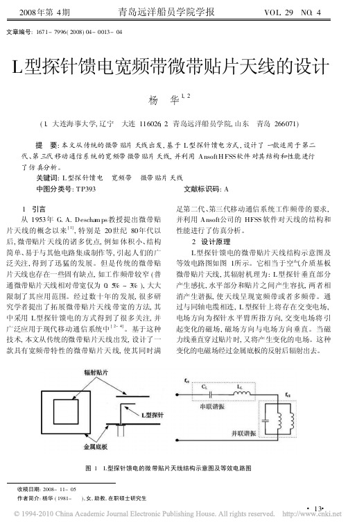
式中 , h 是基板的厚度。 3 仿真结果 利用 A nsof t H FSS 软件对天线结构的主要参 数进行仿真, 经过数次优化后, 该宽频带微带贴片 天线的主要尺寸如表 1 所示 , 仿真的主要结果如 图 3 ~ 图 6 所示。
式中, C 是真空中的光速,
微带线天线馈电原理

微带线天线馈电原理微带线天线馈电原理微带线天线(Microstrip antenna)是一种平板式天线,由于其结构简单、易于制造和调整等优点,在卫星通信、雷达测量等领域得到了广泛应用。
而微带线天线的馈电方式也是很重要的一部分,下面就简单介绍一下微带线天线馈电的原理。
一、微带线天线结构微带线天线由两个主要部分构成:天线贴片和微带线馈线。
天线贴片是由介电材料和金属构成的,其形状和尺寸会对天线的辐射特性产生非常大的影响。
通常情况下,天线贴片的形状是圆形、方形或矩形的。
介电材料通常是PTFE或FR-4等。
微带线馈线是从天线贴片到源或负载之间的导体。
它是由铜箔覆盖在介电基板上,并用印刷电路技术制造而成。
微带线馈线使用也会影响到天线的辐射特性,所以具体的天线设计需要考虑到天线贴片和微带线馈线之间的相互影响。
二、微带线天线的馈电原理通常情况下,微带线天线的馈电方式有两种,一种是通过COAX和微带线过渡来实现馈电的;一种是直接在贴片上开孔,将馈线与贴片相连。
微带线天线的馈电原理可以通过微波模型进行模拟和理解。
在微波模型中,天线贴片是电容,微带线馈线是电感,通过调节它们之间的物理尺寸和位置,可以得到天线的输入阻抗等有关参数。
对于微带线天线来说,其馈电原理主要基于其在等效电路中的表现,即通过开孔或者过渡来实现本质上的电容与电感耦合,从而将微带线的能量转化成为微带线天线所需的电场和磁场,并产生全向或定向的辐射。
三、微带线天线馈电方式的特点1. 传输效率高:与传统天线相比,微带线天线利用电阻较小的铜箔、介质成本较低、简单易制造的技术,使馈电方式更加可靠和传输效率高。
2. 空间利用率高:微带线天线可以利用介质板上的空间进行设计,减少空间占用,提高空间利用率。
3. 频带宽度较宽:微带线馈线传输的电场和磁场能够交错在介质板上,从而产生多种共振模式,实现频段宽带的涵盖,提高天线的频带宽度。
总之,微带线天线馈电方式是微带线天线的重要组成部分,其具有优秀的传输效率、高空间利用率和较宽的频带宽度,能够为无线通信、雷达测量等领域提供更好的通讯和测量技术支持。
《2024年新型级联馈电微带天线设计及应用》范文

《新型级联馈电微带天线设计及应用》篇一一、引言随着无线通信技术的飞速发展,天线作为无线通信系统中的重要组成部分,其性能的优劣直接影响到整个系统的性能。
微带天线因其体积小、重量轻、低剖面、易于集成等优点,在无线通信领域得到了广泛应用。
然而,传统的微带天线存在带宽窄、效率低等问题。
为了解决这些问题,新型级联馈电微带天线设计应运而生。
本文将介绍新型级联馈电微带天线的设计原理、方法及在实际应用中的效果。
二、新型级联馈电微带天线的设计原理及方法新型级联馈电微带天线的设计基于微带天线的基本原理,通过级联馈电的方式,提高天线的带宽和效率。
设计过程中,主要考虑以下几个方面:1. 天线结构的设计:根据实际需求,设计合理的天线结构,包括辐射贴片、介质基板和馈电网络等部分。
其中,辐射贴片采用适当的形状和尺寸,以提高天线的辐射性能。
2. 级联馈电方式的选择:级联馈电是一种通过多个馈电点将信号逐级传输到辐射贴片的方式。
在选择级联馈电方式时,需考虑天线的带宽、增益和辐射效率等因素。
3. 仿真与优化:利用电磁仿真软件对天线进行仿真分析,根据仿真结果对天线结构进行优化,以提高天线的性能。
三、新型级联馈电微带天线的应用新型级联馈电微带天线具有带宽宽、效率高、易于集成等优点,在无线通信领域得到了广泛应用。
以下是几个典型的应用场景:1. 移动通信:在4G、5G等移动通信系统中,新型级联馈电微带天线被广泛应用于基站和移动终端设备中,提高了通信系统的性能和可靠性。
2. 卫星通信:在卫星通信系统中,新型级联馈电微带天线可用于卫星天线阵列中,提高天线的增益和辐射效率,从而提高卫星通信系统的性能。
3. 雷达系统:在雷达系统中,新型级联馈电微带天线可用于提高雷达天线的增益和抗干扰能力,从而提高雷达系统的探测性能。
四、实验结果与分析为了验证新型级联馈电微带天线的性能,我们进行了实验测试和分析。
实验结果表明,新型级联馈电微带天线具有以下优点:1. 带宽宽:新型级联馈电微带天线的带宽比传统微带天线有明显提高,可适应不同频率的要求。
一种采用微带馈电的陷波超宽带天线的设计

图 5开路微 带线长度 的影响 为了全面 的研究天线的性能,图 6给出 了天线分别在 3 、
79 H 、 G z的 辐 射特 性 。从 所 示 的 三 个 辐射 方 向 图可 以看 出 : 在
H面 , 天线具有较好 的全 向辐射特性 , 且在不 同的频率是基本
一
[] F d rl o 2 e ea C mmu ia o s o nct n mmi in Fr p r ado— i C s o . i te ot r s sr n
通 过 用 高频 结 构 仿 真 软件 H S 仿 真 及 优 化 的 比较 , 良 FS 优
的天线的尺寸如下: L 3 m L = 8 L = mm, - m W= = 5 m,g 1mm,s2 Ws9 m,
LI 6 5 =I . mm ,W 1 2 = mm,L2 . mm,W 2 . mm,a mm , =6 5 =0 8 =6
2 1 年 第 5 期 02 ( 第 1 1期 ) 总 2
信 息 通 信
I NFOR ATI M ON & COM MUNI AT ON S C I
2 2 O1
( u . N 1 1 Sm o 2)
一
种采用微 带馈 电的陷波超 宽带天线 的设计
徐 保 林
( 成都理工大学信息科学与技 术学院, 四川 成都 6 0 5 ) 10 9
带线馈 电的超宽带天线, 同时为 了避免 WL AN窄带系统对超 宽带通信 的干扰 ,在多边环形内部 嵌入 开路微带线结构来实
现 特 定 频 段 的 陷 波 特 性 , 使两 系统 能够 协 同工 作 。利 用 仿 真
软件对天线关键结构的参数进 行仿 真比较 ,进而得到 了性能 较好 的参数 , 最终确定方案 的仿真结果达到了设计 的要 求, 而 且该天线 的结构 比较简单, 易于实现 。
微带线馈电的宽带单层贴片天线

摘 要 : 带 贴 片 天 线 已广 泛应 用 于 雷 达 系统 , 中介 绍 了一 种 新 型 背 腔 式 单 层 微 带 贴 片 天 线 , 射 微 文 辐
贴 片 采 用微 带 线 馈 电 , 增 加 工 作 带 宽 , 供 了 两种 不 同 的 贴 片 形 状 , 一 种 是 E 形 贴 片 . 真 及 测 试 结 果 为 提 第 仿 表 明 , 种 单 元在 驻 波 比优 于 2的备 件 下 可 实现 4 的 阻抗 带 宽 , 该 单 元 的 波 瓣 带 宽 较 窄 。 为 抑 制 交 叉 此 5 但
1 i p d n eh n wit o W R≤ 1 5,wihlw R S。 oaiaino s h n 一 】 . d co steo — 4 m e a c a d d hfrVS . t o CO Sp lr t fl st a 。 z o e 5 0 B a r s h p
极 化 , 过在 E形 贴 片上 开 四 个 槽 , 到 了 第二 种 改 进 的 E形 贴 片 。 该 单 元 可 实 现 1 的 频 带 内驻 波 比 优 通 得 4
于 l5 同 时 交 叉极 化 优 于 一 l d _, 5 B。对 C波 段 8 6单 元 实验 小 阵 的测 试 结 果 表 明 , 天 线 在 l. 的 频 ×l 该 79
第 4期 21 O 2年 8门
雷达 科 学 与 技 术
R ada r Sc i eRce and echnol y T og
V O .1 o 1 0 N .4
A ug t 2 2 us 0l
微 带 线 馈 电 的 宽 带 单 层 贴 片 天 线
一种宽带容性馈电小型化微带贴片天线[发明专利]
![一种宽带容性馈电小型化微带贴片天线[发明专利]](https://img.taocdn.com/s3/m/3ad6968e1ed9ad51f11df2cc.png)
专利名称:一种宽带容性馈电小型化微带贴片天线专利类型:发明专利
发明人:袁洪,祁峥东,肖鸿
申请号:CN201510726323.3
申请日:20151029
公开号:CN105244614A
公开日:
20160113
专利内容由知识产权出版社提供
摘要:本发明公开了一种宽带容性馈电小型化微带贴片天线。
本发明将泡沫介质基板置于微带介质基板和接地板中间,增加介质基板厚度,同时降低等效介电常数,拓展天线的工作带宽;在辐射贴片一侧的边缘加载金属短路面,形成开路到短路的驻波结构,天线在与短路面垂直方向的长度为四分之一波长;通过在辐射贴片上开槽,弯曲天线贴片表面激励电流的路径,增加了天线贴片的有效长度,从而使谐振频率降低,实现天线在另一维尺寸的小型化;采用容性贴片耦合馈电,达到良好的阻抗匹配,从而降低天线的等效品质因素,实现天线工作带宽的增加。
本发明克服现有微带贴片天线在兼顾宽频带和小型化方面的不足,具有宽频带、低剖面、尺寸小、重量轻、易于加工的优点。
申请人:中国船舶重工集团公司第七二四研究所
地址:210003 江苏省南京市中山北路346号
国籍:CN
更多信息请下载全文后查看。
24GHz微带贴片天线设计-毕业论文

---文档均为word文档,下载后可直接编辑使用亦可打印---摘要根据矩形贴片天线相关知识,设计出一款1×4的24GHz阵列贴片天线,此天线可以应用于交通测速以及汽车智能驾驶等方面。
首先是使用微带线馈电的方法建立单元贴片天线模型,进行优化仿真后得到最佳的单元贴片天线模型,然后在单元贴片天线的基础上,设计出合适的馈电馈电网络。
再通过仿真优化得到最佳的参数,从而设计出24GHz的阵列贴片天线。
并对天线设计进一步展望。
通过HFSS软件仿真设计,得到了一款1×4的阵列天线,回波损耗S11<-20dB,馈电点的输入阻抗值为50Ω,驻波比约为1.2,最大增益方向的增益为13.6dB,和之前所定的设计指标比较符合。
关键词:微带贴片天线;阵列天线;阻抗匹配; 方向图AbstractAccording to the knowledge of the rectangular patch antenna, a 1×4 24 GHz array patch antenna was designed. This antenna can be used in traffic speed measurement and intelligent driving of automobiles. The first is to use the method of microstrip line feeding to establish the unit patch antenna model, optimize the simulation to obtain the best unit patch antenna model, and then design a suitable feed power feed network based on the unit patch antenna. . Then the optimal parameters are obtained through simulation optimization to design a 24 GHz array patch antenna.Through the HFSS software simulation design, a 1×4 array antenna was obtained with a return loss S11<-20dB, a feed point input impedance of 50Ω, a standing wave ratio of approximately 1.2, and a maximum gain gain of 13.6dB. To meet the requirements of design indicators.Keywords: microstrip patch antenna; array antenna; Impedance matching;Direction pattern第1章绪论1.1论文的研究背景及意义毫米波(millimeter wave )是波长为1~10毫米的电磁波,它的波长处于微波与远红外波相交叠的波长范围,所以同时具有两种波谱的特点。
- 1、下载文档前请自行甄别文档内容的完整性,平台不提供额外的编辑、内容补充、找答案等附加服务。
- 2、"仅部分预览"的文档,不可在线预览部分如存在完整性等问题,可反馈申请退款(可完整预览的文档不适用该条件!)。
- 3、如文档侵犯您的权益,请联系客服反馈,我们会尽快为您处理(人工客服工作时间:9:00-18:30)。
外形小、成本低的天线可用于许多现代通信系统中。
微带贴片天线代表一系列的小型天线,它们具有等角性质和已与通信系统的印刷电路集成在一起的优点。
通过采用简单明了的传输线模型,建立微带线嵌入馈电(inset-fed)贴片天线的精确模型并对之进行分析已成为可能。
另外,通过应用曲线拟合公式,也可以确定50Ω输入阻抗所需的精确嵌入长度。
馈电机制在微带贴片天线设计中扮演了重要角色。
微带天线可以由同轴探针或嵌入的微带线来馈电,同轴探针馈电在有源天线应用中具有优势,而微带线馈电则是适合于开发高增益微带阵列天线。
对于这两种情况,探针的位置或嵌入的长度都将决定输入阻抗的大小。
已通过各种各样的模型,包括传输线模型和空腔模型,以及通过全波分析对同轴探针馈电的贴片天线分输入阻抗特性进行了分析。
无论从实验上还是从理论上,都证明了同轴探针馈电贴片天线的输入阻抗特性遵守三角函数:cos2[π(y0/L)],其中,L等于贴片长度,y0等于从边缘沿着贴片长度L方向的馈电位置。
另一方面,从实验上也证明在低介电常数材料上,嵌入馈电的探针天线的输入阻抗表现为以下函数的4阶特性:cos4[π(y0/L)]。
幸运的是,现已开发出一种简单的分析方法,该方法利用传输线模型来获得嵌入馈电微带贴片天线的输入阻抗。
利用这种方法,在使用现代薄介电电路板材料时,可引用曲线拟合公式来确定嵌入长度,以便实现50Ω的输入阻抗。
图1是嵌入馈电微带贴片天线的图示。
参数εr、h、L、W、w< SUB >f< /SUB >和y0分别代表基板的介电常数、厚度、贴片长度、贴片宽度、馈线宽度和馈线嵌入距离。
嵌入馈电微带贴片天线的输入阻抗主要取决于嵌入距离y0,并在某种程度上取决于嵌入宽度(馈线与贴片导线之间的间距)。
嵌入长度的变化不会在谐振频率上产生任何改变,但是嵌入宽度的变化却会导致谐振频率的改变。
因此,在下面的讨论中,贴片导线与馈线之间的间距是保持不变,等于馈线宽度。
在与嵌入长度有关的谐振频率下的输入阻抗的变化,将在下列讨论中被看作各种参数的函数。
假设贴片天线可分成四个区域,那么可将它建模成一系列带有不同长度辐射槽的传输线(图2),表中列举了这三个传输线的参数(宽度和长度)和这三个辐射槽的宽度和长度。
根据早期提出的方法,对一个具有εr=2.42、h=0.127cm、w=4.04cm、L=5.94cm和y0=0.99cm 参数的贴片天线进行了分析。
图3显示了采用这里所提到的传输线模型方法所得到的结果,并将它与采用商用计算机辅助工程电磁(EM)仿真器得到的数据进行了比较。
即使谐振频率有点漂移,传输线模型还是能非常接近地跟踪EM仿真器预测的回波损耗曲线。
谐振频率上的这个微小漂移,是由于没有考虑嵌入馈线与贴片之间的不连续性而导致的。
在各种εr(2 ≤εr≤10)值下利用传输线模型对贴片进行参数研究。
图4表明了在边缘(y0=0)处,由微带线馈电的矩形微带贴片天线具有更高的输入阻抗,对于不同的εr值,其变化大约从150到450Ω。
另外从中也可以观察到,与同轴探针馈电的贴片天线相比,当嵌入位置从贴片边缘向中心移动时,输入阻抗迅速下降。
这些参数的研究已被用来推导如式(1)的曲线拟合公式,以便确定精确的嵌入长度,从而为通常使用的薄介电基板上实现50Ω输入阻抗。
用εr=5.0、h=0.127cm、W=4.1325cm、L=2.8106cm、y0=0.9009cm的贴片天线对该公式的精确性已进行了验证。
为确认公式的有效性,采用EM仿真器对贴片进行分析。
图5给出了由传输线模型产生的结果与EM仿真器预测结果之间的对比。
尽管在这两组数据中谐振频率有1%的偏移,但用这两种方法预测的回波损耗曲线还是具有很明显的紧密一致性。
作者:M. Ramesh,K.B. Yip。