固体电子器件SolidStateElectronicDevices
电子器件英语词汇表

电子器件英语词汇表Electronic Devices English Vocabulary ListIntroduction:In the ever-evolving world of technology, electronic devices play a vital role in our daily lives. From smartphones to laptops, these devices have become an integral part of our communication, entertainment, and work. To better understand this field, it is important to familiarize ourselves with the English vocabulary related to electronic devices. In this article, we will explore a comprehensive list of commonly used terms in this domain.1. Hardware Terminology:1.1 Processor/Central Processing Unit (CPU):The CPU serves as the brain of a computer, executing instructions and carrying out calculations.1.2 Random Access Memory (RAM):RAM is a type of volatile memory that temporarily stores data for active programs.1.3 Solid State Drive (SSD):SSD is a storage device that uses integrated circuits to store data persistently.1.4 Graphics Processing Unit (GPU):The GPU is responsible for rendering images, videos, and animations, making it essential for high-quality visuals in electronic devices.1.5 Motherboard:The motherboard is the main printed circuit board (PCB) that houses vital components of a computer or electronic device.1.6 Power Supply Unit (PSU):The PSU provides electrical power to the other components of a computer or electronic device.1.7 Display:The display refers to the screen or monitor that visually presents information to the user.1.8 Keyboard:A keyboard is an input device that enables users to input text and commands into a computer or electronic device.1.9 Mouse:A mouse is another input device that allows users to control the cursor on the screen.2. Software Terminology:2.1 Operating System (OS):An OS is the software that manages computer hardware and software resources, providing a stable interface for users.2.2 Application:An application, also known as software or program, is designed to perform specific tasks on a computer or electronic device.2.3 Firmware:Firmware refers to software that is embedded in electronic devices, providing low-level control and functionality.2.4 Driver:A driver is software that enables communication between an operating system and a specific hardware device.2.5 Antivirus:Antivirus software helps protect electronic devices from malware, viruses, and other security threats.2.6 Browser:A browser is designed to access and display websites and webpages on the internet.3. Networking Terminology:3.1 Wi-Fi:Wi-Fi is a wireless networking technology that allows electronic devices to connect to the internet or other devices without using physical wired connections.3.2 Ethernet:Ethernet is a standard networking technology that uses wired connections to connect devices in a local area network (LAN).3.3 Router:A router is a device that forwards data packets between computer networks, ensuring efficient communication within a network.3.4 Bluetooth:Bluetooth is a wireless technology that enables short-range communication and data transfer between electronic devices.3.5 IP Address:An IP address is a unique numerical label assigned to each device connected to a computer network, facilitating its identification and communication.4. Mobile Devices Terminology:4.1 Smartphone:A smartphone is a mobile device that combines the functionality of a phone with other features, such as internet access, multimedia capabilities, and various applications.4.2 Tablet:A tablet is a portable computing device with a touchscreen display, similar to a smartphone but with a larger screen size.4.3 E-reader:An e-reader is a device specifically designed for reading electronic books (e-books) and other digital publications.4.4 Wearable Devices:Wearable devices, such as smartwatches and fitness trackers, are worn on the body and provide functionalities like health monitoring, notifications, and communication.Conclusion:This article has provided a comprehensive English vocabulary list related to electronic devices. By familiarizing ourselves with these terms, we can enhance our understanding of this field and effectively communicate in English when discussing electronic devices. As technology continues to advance, staying up-to-date with relevant terminology is essential for both personal and professional purposes.。
Solid State Electronic Devices

Solid State Electronic Devices : The Fundamentals and ApplicationsSolid state electronic devices are an essential part of modern technology. They are the basis for many electronic devices, such as computers, cell phones, and televisions. These devices are based on the principles of solid-state physics, which focuses on the study of materials and their properties.Solid state electronic devices, such as transistors, diodes, and integrated circuits, have revolutionized the way we live and work. They have made it possible to create smaller, faster, and more complex electronic devices. This article will explain the fundamental principles of solid-state electronic devices, their applications, and the future of solid-state electronics.The Physics ofSolid-state electronic devices are electronic components that are made from solid materials, such as semiconductor materials. A semiconductor material is one that has electrical conductivity between that of a conductor and an insulator. The most widely used semiconductor material is silicon, although other materials, such as germanium and gallium arsenide, are also used.The behavior of semiconductors is governed by their electronic properties, such as the energy band structure and the distribution of electrons and holes. These properties are determined by the arrangement of atoms in the crystal lattice structure of the material. The electronic properties of a semiconductor can be manipulated by doping it with impurities.Doping means intentionally introducing impurities or dopants into a semiconductor to modify its electrical properties. Two types of doping are used in semiconductors: n-type and p-type doping. N-type doping is the introduction of impurities with extra electrons, such as phosphorus or arsenic. P-type doping is the introduction of impurities with missing electrons, such as boron.When a semiconductor is doped with n-type impurities, it becomes an n-type semiconductor, which has a surplus of negatively charged electrons. When a semiconductor is doped with p-type impurities, it becomes a p-type semiconductor, which has a deficit of negatively charged electrons. The interaction between these two types of semiconductors is the basis of many solid-state electronic devices.The Applications ofSolid state electronic devices have many applications, from digital circuits to power electronics. They are used in the following applications:1. Digital CircuitsDigital circuits are circuits that use a binary system of 0s and 1s to represent information. Solid state electronic devices, such as diodes and transistors, are used to build digital circuits. Integrated circuits, which are made up of millions of transistors on a single chip, are used in digital circuits to perform billions of calculations in seconds.2. Power ElectronicsPower electronics involve the use of solid state electronic devices to convert electrical energy from one form to another. They are used in a wide range of applications, such as motor control, renewable energy systems, and electric vehicles. Power electronic devices, such as rectifiers, inverters, and DC-DC converters, are used in power electronics.3. OptoelectronicsOptoelectronics involves the use of solid state electronic devices to control and manipulate light. They are used in a wide range of applications, such as fiber optics, displays, and solar cells. Optoelectronic devices, such as LEDs, laser diodes, and photodetectors, are used in optoelectronics.The Future of Solid State ElectronicsSolid state electronics have come a long way since the invention of the transistor. However, there is still room for improvement. Future developments in solid state electronics will focus on the following areas:1. NanotechnologyNanotechnology involves the manipulation of matter on an atomic, molecular, and supramolecular scale. The use of nanotechnology in solid state electronics will lead to the development of smaller, faster, and more efficient devices.2. Quantum ComputingQuantum computing involves the use of quantum phenomena, such as superposition and entanglement, to perform calculations. The development of quantum computing will revolutionize the field of solid state electronics, leading to the development of new types of devices.3. Energy EfficiencyThe development of more energy-efficient solid state electronic devices is a priority, as the demand for energy continues to grow. The use of renewable energy sources, such as solar and wind power, will require the development of more efficient power electronic devices.ConclusionSolid state electronic devices have revolutionized the way we live and work. They are the basis for many electronic devices that we use every day. The principles of solid-state physics govern the behavior of these devices, and their applications are wide-ranging. The future of solid state electronics looks bright, with developments in nanotechnology, quantum computing, and energy efficiency leading the way.。
国外光学电子类核心期刊

序 刊名
号
中文译名
中图刊号 出版国
Journal of magnetism and magnetic
1
磁学和磁性材料杂志
materials
2 Electronics letters
电子学快报
536LB002 736C0061
荷兰 英国
3 IEEE transactions on magnetics
IEEE 磁学汇刊
IEEE 通信汇刊 IEEE-TM S 电子材料杂志 IEEE 信号处理汇刊 IEEE 通信选题杂志 IEEE 应用超导汇刊 IEEE 天线与传播汇刊 微电子工程 半导体科学与技术 IEEE 固态电路杂志 IEEE 微机电系统杂志 微电子学可靠性 IEEE 无线通信杂志 IEEE 无线通信处理杂志
730B0001TCO
537LB053 537C0075 537B0001 546B00 11 798B0072 537LB010 537B0002
14 Journal of lightwave technology
光波技术杂志
15 Journal of the American Society for Mass 美国质谱学会志
中文译名
中图刊号
出版
IEEE transactions on circuits and systems. Ⅰ, Regular IEEE 电路与系统汇刊.第 1 辑,
21 p ap ers
一般论文
730B0001TCS1
美国
IEEE transactions on circuits and systems for video IEEE 视频技术电路与系统汇刊 22
28 briefs
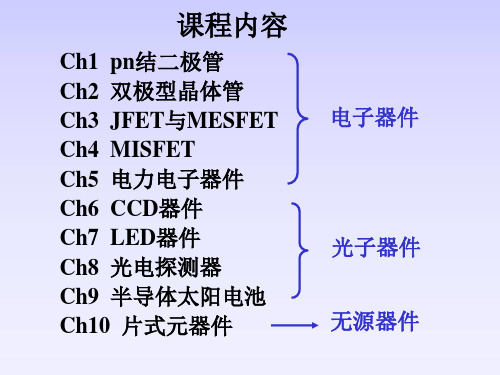
固体电子器件

《固体电子器件》课程教学大纲一、课程说明(一)课程名称、所属专业、课程性质、学分课程名称:半导体器件物理所属专业:微电子科学与工程课程性质:专业必修课学分:4学分(二)课程简介、目标与任务【课程简介】本课程的适用对象是电子工程专业、微电子学专业的本科生,也可供对固体电子器件感兴趣的学生和科技工作者作为参考读本。
本书的主要内容是半导体器件(亦称固体电子器件)的工作原理,基本涵盖了所有的器件大类,反映了现代半导体器件的基础理论、工作原理、二级效应以及发展趋势;同时对许多新型器件和制造技术也有所介绍。
本课程在内容的安排上力求使那些具有物理背景知识的高年级学生对专业知识有更为深入的理解,从而使他们能够阅读关于新器件及其应用的参考文献。
【目标与任务】本课程有两个基本目标和任务:一是对七大类半导体器件的结构、工作原理、特性做全面深入的分析与阐述,对相关的半导体材料和制造工艺也有述及;二是介绍新型纳电子器件及其基本分析方法,这样既便于与电子线路和电子系统等相关课程衔接,也使学生具备分析、设计新型器件的基本能力和方法。
(三)先修课程与后续课程本课程的先修课程包括:半导体材料,半导体物理学,微电子制造工艺。
本课程是后续集成电路分析与设计、微电子专业实验等课程的基础。
(四)教材与主要参考书【课程教材】(1)英文版:Ben G. Streetman and Sanjay Banerjee, Solid State Electronic Devices(Seventh edition), Pearson Education, Inc., 2015. ISBN 978-0-13-335603-8.(2)中文版:Ben G. Streetman著,杨建红译,《固体电子器件》,电子工业出版社,2016年(在版)。
【主要参考书】施敏(美)著,耿莉译,半导体器件物理,西安交通大学出版社,2013年。
ISBN 978-7-5605-2596-9.二、课程内容与安排第1章晶体性质和半导体生长(略讲,无计划学时)1-1 常用半导体材料的晶体结构1-2 硅块状晶体生长电子级硅(EGS)原料的制备;单晶Si的Czochralski制备方法;Si掺杂技术。
固态电子器件ppt课件
所以
n(xp ) ni exp
EpF EiP qVA
/ kT
np
exp(
qVA KT
)
(xn)处少子空穴浓度,同理可得:
p(x
n
)
pn
exp(
qVA KT
)
空间电荷内及其边界电子与空穴浓度的积:
n(x)
p(x
)
n(xp
)
p(x
n
)
ni2
exp(
qVA KT
)
a. 非平衡pn结空间电荷区及其边界电子与空穴 浓度的积相等,且是偏置电压的e指数函数。
P区
Eip
Ei(x)
qVD
Ein
N区
ψ(x)
VD
-xp
-xn
费米能级:
对于平衡pn结,只要确定费米能级位置,则可得到其能带结构。
设ψ(-xp)=0,有
Ei(x) = Eip―qψ(x)
式中Eip为中性p区本征费米能级,对上式微分有
1 dEi (x) d(x) (x)
q dx
dx
利用上式及
p(x)
n(x) ni exp EnF Ei (x) / KT p(x) ni exp Ei (x) EpF / KT
空间电荷区边界载流子浓度:
仍设pn结外加偏压为VA,VA>0为正偏,VA<0为反偏
(-xp)处少子电子浓度:
因为 EnF = EpF + qVA ,Ei(-xp) =Ei p—中性p区本征费米能级
7. 电子和空穴各自的扩散(扩散流)与漂移(漂移流)相抵消时,正、负空间电荷量、
正、负空间电荷区宽度、自建电场、空间电荷区内电子和空穴分布达到动态平衡,形
固态电子器件与集成电路

Reference(半导体物理与器件) (半导体物理与器件)
1. 《Principles of Semiconductor Devices 》 Principles Bart Van Zeghbroeck (/~bart/book/) /~bart/book/ 2. 《Solid State Electronic Devices》 Ben G. Streetman & Sanjay Banerjee 3. 《Semiconductor Physics and Devices Basic Principles Semiconductor Principles》Donald A. Neamen 4.《Semiconductor Devices 》Simon M. Sze (施敏) Simon 5.《 Fundamentals of Solid State Electronics Electronics》 Chih Tang Sah ( 萨支唐) 6.《 Physics of Semiconductor Devices》 》Simon M. Sze
Solid classified from conduct>106(Ωcm -1 Ωcm) conductor: 106~104(Ωcm)-1 Ω <10-10(Ωcm -1 Ωcm) semiconductor: 104~10-10(Ωcm)-1 (Ω insulator:
The scaling of MOSFETs started in the seventies(70). Since then, the initial 10 micron gatelength of the devices was gradually reduced by about a factor two every five years, while in 2000 MOSFETs with a 0.18 micron gatelength were manufactured on a large scale. This scaling is expected to continue well into the 21st century, as devices with a gatelength smaller than 30 nm have already been demonstrated. While the size reduction is a minimum condition when scaling MOSFETs, successful scaling also requires the reduction of all the other dimensions of the device so that the device indeed delivers superior performance. Devices with record gate lengths are typically not fully scaled, so that several years go by until the large large-scale production of such device takes place.
固态电子器件课后题答案5

© 2006 Pearson Education, Inc., Upper Saddle River, NJ. All rights reserved. This material is protected under all copyright laws as they© 2006 Pearson Education, Inc., Upper Saddle River, NJ. All rights reserved. This material is protected under all copyright laws as they© 2006 Pearson Education, Inc., Upper Saddle River, NJ. All rights reserved. This material is protected under all copyright laws as they© 2006 Pearson Education, Inc., Upper Saddle River, NJ. All rights reserved. This material is protected under all copyright laws as they© 2006 Pearson Education, Inc., Upper Saddle River, NJ. All rights reserved. This material is protected under all copyright laws as they© 2006 Pearson Education, Inc., Upper Saddle River, NJ. All rights reserved. This material is protected under all copyright laws as they© 2006 Pearson Education, Inc., Upper Saddle River, NJ. All rights reserved. This material is protected under all copyright laws as they© 2006 Pearson Education, Inc., Upper Saddle River, NJ. All rights reserved. This material is protected under all copyright laws as they© 2006 Pearson Education, Inc., Upper Saddle River, NJ. All rights reserved. This material is protected under all copyright laws as they© 2006 Pearson Education, Inc., Upper Saddle River, NJ. All rights reserved. This material is protected under all copyright laws as they。
微电子与固体电子学专业博士研究生培养方案
中山大学微电子学与固体电子学()专业博士研究生培养方案(学术型)一、学科介绍本学科涉及微纳电子学、柔性显示与微显示技术、微纳光电子器件及集成、宽禁带半导体材料与器件、SOC设计与应用、集成电路设计与微电子技术、纳微电子器件与技术、微电子、光电子材料与集成器件、微纳能量转换器件、薄膜电子器件与技术、真空纳微电子学、新型平板显示技术、光电子器件及集成、电力电子中的微电子技术、电子材料与敏感元器件、集成电路设计与微电子应用等研究方向。
二、培养目标本专业培养德、智、体全面发展的微电子学与固体电子学方面的高级专门人才。
要求学生遵守中华人民共和国宪法和法律,具有为科学事业献身的精神、良好的品德和科学修养、健康的身体和良好的心理素质;在本学科掌握坚实宽广的基础理论和系统深入的专业知识,掌握一至两门外国语,具有独立从事科学研究、教学或独立负担专业技术工作的能力,在微电子学与固体电子学或相关科学领域的研究或应用上做出创造性成果,成为为社会主义建设服务的高层次专门人才。
三、学习年限1、三年制博士研究生:三年。
2、直读博士研究生:五年。
3、硕博连读研究生:五年。
四、培养方式微电子学与固体电子学专业博士的培养按照中山大学全日制博士研究生的培养方式进行,学生按照要求完成规定学分、规定的学术交流活动和社会实践活动,在导师或导师组的指导下完成博士学位论文。
培养的学生要求扎实掌握本专业的理论和技术基础,掌握本专业发展前沿动态。
五、课程设置六、必修环节培养要求按《中山大学学位与研究生教育工作手册》和《物理科学与工程技术学院研究生培养管理条例》有关规定执行。
七、考核按培养方案的要求,通过课程考试取得规定学分并通过学位论文答辩,经校学位评定委员会批准,授予微电子学与固体电子学专业的工学博士学位。
八、学位论文和答辩按《物理科学与工程技术学院研究生培养管理条例》有关规定执行。
九、必读和选读书目1.半导体物理与器件——基本原理(Semiconductor Physics and Devices : Basic Principles), Donald A.Neamen, McGraw-Hill Companies, Inc, 清华大学出版社,2003。
- 1、下载文档前请自行甄别文档内容的完整性,平台不提供额外的编辑、内容补充、找答案等附加服务。
- 2、"仅部分预览"的文档,不可在线预览部分如存在完整性等问题,可反馈申请退款(可完整预览的文档不适用该条件!)。
- 3、如文档侵犯您的权益,请联系客服反馈,我们会尽快为您处理(人工客服工作时间:9:00-18:30)。
加 工 液 晶 显 示器
多晶
在小区域内 完全有序
多 晶 硅 -太阳能电池
单晶
整个晶体中 排列有序
单 晶 硅 -电 子 器件
集成电路制造
2 晶体结构
( 1) 晶 体 的 共性
①均匀性; ④ 多 面 体 外 形;
②各向异性; ⑤对称性;
③熔点固定; ⑥衍射性。
2 晶体结构
(2)硅的结构和特性
+4 +4
锗 、 硅 和 砷 化镓能 带结构 的简约 布里渊 图示。
导体 < 10-3
半导体 10-3~109
绝缘体 >109
1绪论
(1)导电性
➢
温 度 可 以 显 著改变 半导体 导电能 力;
➢
微 量 杂 质 可 以显著 改变半 导体导 电能力 ;
➢ 光 照 、 磁 场 、电场 等外界 因素也 可显著 改变半 导体的 导电能 力; ➢ 电 子 和 空 穴 晶体结构
4 半 导 体 中 杂 质和 缺陷能 级 5 载流子
3 半 导 体 中 的 电子 状态
6 载流子的浓度
7 载流子的输运
1绪论
什么是半导体?
( 1) 导 电 性
➢ 电 阻 率 介 于 导体与 绝缘体 之间;
表 1 导体、半导体和绝缘体的电阻率范围
材料 电阻率ρ(Ωcm)
+4 +4
2 晶体结构
(3)晶向和晶面
2 晶体结构
(4) 硅片鉴别方法
[110]
第一篇 半导体物理基础
1绪 论 2 晶体结构
4 半 导 体 中 杂 质和 缺陷能 级 5 载流子
3 半 导 体 中 的 电子 状态
6 载流子的浓度
7 载流子的输运
3 半导体中的电子状态
电 子 受 到 原 子核和 其他电 子的共 同作用 。 静 电 引 力 (库 仑力) ,使电 子只能 在围绕 原子核 的轨道 上运动 。
半导体是一类性质可受光、热、磁、电,微量杂质等作用而改变其性质的材料。
1绪论
(2)分类- 组成
➢ 元素半导体 ➢ 无 机 化 合 物 半导体 ➢ 有 机 化 合 物 半导体
➢ 液态半导体
1绪论
按 原 子 或 分 子排列 规律性 分:
(2)分类
无定形(非晶)
不存在长程有序
或
应 用
几个尺度内有序
无 定 形 硅 薄 膜-
+
3 半导体中的电子状态
(3) 硅 的 能 带 对 于 硅 或 锗 晶体 ,由于 sp³轨 道杂化 ,本应 统一的 价带分 成上、 下各包 含2N个 量子态 的能带 。
下 能 带恰 好容纳 4N个价 电子而 形成满 带,上 能带则 成为没 有价电 子占据 的空带 。
3 半导体中的电子状态
(3) 硅 的 能 带
(1) 单 个 原 子 中 的电 子
轨道: 电 子 云 在 空 间分 布几率 最大值 ,即轨 道上, 电子出 现的几 率最大 。
原子核
电子
+
能级
E r
3 半导体中的电子状态
(2) 晶 体 中 的 电 子
能带
能级
由于晶体中原子的周期 性排列而使电子不再为单个 原子所有的现象,称为电子 共有化。
+
+
+