STM32芯片烧写方法
如何通过JLINK烧写STM32程序

百为技术有限公司
7、 此时打开要烧写到 STM32 的 hex 文件
打开后如下图示:
百为技术有限公司
8、 然后点击 Target->Program & Verify 进行烧写
9、 弹出如下界面表示完成烧写
百为技术有限公司
如何通过 JLINK 烧写 STM32 程序
1、 首先安装 JLINK 驱动,Setup_JLinkARM_V420p.exe
2、 从开始程序菜单打开 J-FLASH 程序, 所有程序->SEGGER->J-Link ARM V4.20p->J-Flash ARM
百为技术有限公司
3、 点击 Options->Project settings
百为技术有限公司
4、 弹出如下界面,进入 CPU 页面,选择 Device ST STM32F103ZE,点击确定
百为技术有限公司
5、 用 JLINK 连接开发板和 PC,点击 Target->Connet 进行连接。
百为技术有限ห้องสมุดไป่ตู้司
6、 连接完成后,可以看到类似如下信息: - J-Link found 2 JTAG devices. Core ID: 0x3BA00477 (Cortex-M3) - Connected successfully
STM32_FLASH的3种烧写方式
ST ARM 芯片的FLASH 烧写方法一、 RVMDK+ULink2(ST ‐Link2、JLink)注:适用于所有的ARM芯片,但硬件上必须有JTAG 接口。
使用仿真器+ARM 开发环境,是最常用的一种方法。
该方法适用于硬件上留有JTAG/SWD 接口,如有源程序代码,可以直接编译下载;另外使用RVMDK+ULink2也可直接下载.hex 文件,操作如下。
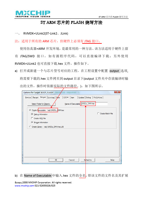
a) 打开或新建一个与芯片型号对应的工程,在工程设置中配置output 选项,将需要下载的.hex 文件拷贝到output 目录下(output 文件夹中存放编译时输),如下图所示。
©2008 MXCHIP Corporation. All rights reserved.b) 在Name of Executable:中输入.hex名,如上图所示。
c) 配置Utilities 选项,选中Use Target Driver for Flash Programming 项(默认情所示。
©2008 MXCHIP Corporation. All rights reserved.d) c)添加Flash Programming Algorithm ,即添加与目标芯片对应的Flash 编程算法,如下图所示。
e)以上步骤完成后,连接仿真器和目标板,即可把目标程序烧写到芯片的Flash中。
二、 串口+ISP软件注:适用于带有ISP功能的ARM芯片,需要硬件上留有COM接口,且芯片的启动模式可设置。
用户的ARM系列芯片带有ISP(在系统中编程)功能,则可使用其ISP功能,通过串口和ISP软件来下载.bin文件。
下面以STM32系列芯片为例(STM32全系列芯片都带有ISP功能),演示该烧写方法。
a)将USART1口连接到PC的COM口(通常ISP使用的UART口都是芯片的第一个UART口),设置芯片的启动模式为System Memary模式(BOOT1为0,©2008 MXCHIP Corporation. All rights reserved.BOOT0为1)。
STM32烧写程序步骤
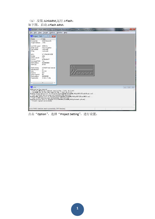
(1).安装JLinkARM,运行J-Flash:
如下图,启动J-Flash ARM:
点击“Option”,选择“Project Setting”,进行设置:
选择烧写方式为SWD:
选择CPU型号为STM32F103C8:
设置后会提示下图所示信息:
(2).连接目标板
将J-LINK一端通过USB线和PC连接起来,另一端按所给的接线图和JTAG口相连,接线图如下:
给工业节点提供12V电源,然后如下图所示点击“connect”:
连接成功后会提示下图所示信息:
(3).下载HEX文件
点击File下的open,打开Hex文件:
点击Target,选择Auto,将下载Hex到ARM:程序下载进度条显示如下:
下图为程序下载成功:
点击”确定”按钮,后按下F9按键,等待一会,程序将运行起来,在下图的状态栏提示如下字符串才能说明程序真正烧进去:
- Target application started。
【STM32】如何将资源烧写至外部flash,如spi-flash
【STM32】如何将资源烧写⾄外部flash,如spi-flashSTM32将资源烧写⾄外部flash⽅式⼤致分为通过IDE与应⽤程序⼀起和通过CubeProgranmmer单独烧写两种:⽅式⼀、使⽤IDE加载烧写算法,烧录应⽤程序时⼀并写⼊,具体就是修改分散加载链接脚本将部分常量数据移⾄外部flash,烧写算法制作⼯程如下主要实现两个⽂件,接⼝实现⽂件 <FLashPrg.c> 和设备描述⽂件 <FLashPrg.c>FLashPrg.c1/**************************************************************************//**2 * @file FlashDev.c3 * @brief Flash Device Description for New Device Flash4 * @version V1.0.05 * @date 10. January 20186 ******************************************************************************/7/*8 * Copyright (c) 2010-2018 Arm Limited. All rights reserved.9 *10 * SPDX-License-Identifier: Apache-2.011 *12 * Licensed under the Apache License, Version 2.0 (the License); you may13 * not use this file except in compliance with the License.14 * You may obtain a copy of the License at15 *16 * /licenses/LICENSE-2.017 *18 * Unless required by applicable law or agreed to in writing, software19 * distributed under the License is distributed on an AS IS BASIS, WITHOUT20 * WARRANTIES OR CONDITIONS OF ANY KIND, either express or implied.21 * See the License for the specific language governing permissions and22 * limitations under the License.23*/2425 #include "..\FlashOS.H"// FlashOS Structures262728struct FlashDevice const FlashDevice = {29 FLASH_DRV_VERS, // Driver Version, do not modify!30"STM32F429_W25Q128", // Device Name31 EXTSPI, // Device Type320x90000000, // Device Start Address330x01000000, // Device Size in Bytes (256kB)34256, // Programming Page Size350, // Reserved, must be 0360xFF, // Initial Content of Erased Memory37100, // Program Page Timeout 100 mSec383000, // Erase Sector Timeout 3000 mSec3940// Specify Size and Address of Sectors410x001000, 0x000000, // Sector Size 8kB (8 Sectors)42// 0x010000, 0x010000, // Sector Size 64kB (2 Sectors)43// 0x002000, 0x030000, // Sector Size 8kB (8 Sectors)44 SECTOR_END45 };FLashPrg.c1/**************************************************************************//**2 * @file FlashPrg.c3 * @brief Flash Programming Functions adapted for New Device Flash4 * @version V1.0.05 * @date 10. January 20186 ******************************************************************************/7/*8 * Copyright (c) 2010-2018 Arm Limited. All rights reserved.9 *10 * SPDX-License-Identifier: Apache-2.011 *12 * Licensed under the Apache License, Version 2.0 (the License); you may13 * not use this file except in compliance with the License.14 * You may obtain a copy of the License at15 *16 * /licenses/LICENSE-2.017 *18 * Unless required by applicable law or agreed to in writing, software19 * distributed under the License is distributed on an AS IS BASIS, WITHOUT20 * WARRANTIES OR CONDITIONS OF ANY KIND, either express or implied.21 * See the License for the specific language governing permissions and22 * limitations under the License.23*/2425 #include "..\FlashOS.H"// FlashOS Structures26 #include ".\flash\bsp_spi_flash.h"272829#define PAGE_SIZE SPI_FLASH_PageSize303132 uint8_t auxBuf[PAGE_SIZE];33 uint32_t baseAddr;3435/*36 Mandatory Flash Programming Functions (Called by FlashOS):37 int Init (unsigned long adr, // Initialize Flash38 unsigned long clk,39 unsigned long fnc);40 int UnInit (unsigned long fnc); // De-initialize Flash41 int EraseSector (unsigned long adr); // Erase Sector Function42 int ProgramPage (unsigned long adr, // Program Page Function43 unsigned long sz,44 unsigned char *buf);4546 Optional Flash Programming Functions (Called by FlashOS):47 int BlankCheck (unsigned long adr, // Blank Check48 unsigned long sz,49 unsigned char pat);50 int EraseChip (void); // Erase complete Device51 unsigned long Verify (unsigned long adr, // Verify Function52 unsigned long sz,53 unsigned char *buf);5455 - BlanckCheck is necessary if Flash space is not mapped into CPU memory space56 - Verify is necessary if Flash space is not mapped into CPU memory space57 - if EraseChip is not provided than EraseSector for all sectors is called58*/596061/*62 * Initialize Flash Programming Functions63 * Parameter: adr: Device Base Address64 * clk: Clock Frequency (Hz)65 * fnc: Function Code (1 - Erase, 2 - Program, 3 - Verify)66 * Return Value: 0 - OK, 1 - Failed67*/6869int Init (unsigned long adr, unsigned long clk, unsigned long fnc)70 {71/* Add your Code */72 baseAddr = adr;73 SPI_FLASH_Init();74return (0); // Finished without Errors75 }767778/*79 * De-Initialize Flash Programming Functions80 * Parameter: fnc: Function Code (1 - Erase, 2 - Program, 3 - Verify)81 * Return Value: 0 - OK, 1 - Failed82*/8384int UnInit (unsigned long fnc)85 {86/* Add your Code */87return (0); // Finished without Errors88 }899091/*92 * Erase complete Flash Memory93 * Return Value: 0 - OK, 1 - Failed94*/9596int EraseChip (void)97 {98/* Add your Code */99 SPI_FLASH_BulkErase();100return (0); // Finished without Errors101 }102103104/*105 * Erase Sector in Flash Memory106 * Parameter: adr: Sector Address107 * Return Value: 0 - OK, 1 - Failed108*/109110int EraseSector (unsigned long adr)111 {112/* Add your Code */113 SPI_FLASH_SectorErase(adr - baseAddr);114return (0); // Finished without Errors115 }116117118/*119 * Program Page in Flash Memory120 * Parameter: adr: Page Start Address121 * sz: Page Size122 * buf: Page Data123 * Return Value: 0 - OK, 1 - Failed124*/125126int ProgramPage (unsigned long adr, unsigned long sz, unsigned char *buf)127 {128/* Add your Code */129 SPI_FLASH_PageWrite(buf, adr - baseAddr, sz);130return (0); // Finished without Errors131 }132133/*134 * Verify Flash Contents135 * Parameter: adr: Start Address136 * sz: Size (in bytes)137 * buf: Data138 * Return Value: (adr+sz) - OK, Failed Address139*/140141/*142 Verify function is obsolete because all other function leave143 the SPIFI in memory mode so a memory compare could be used.144*/145 unsigned long Verify (unsigned long adr, unsigned long sz, unsigned char *buf)146 {147int i;148 SPI_FLASH_BufferRead(auxBuf, adr - baseAddr, sz);149for (i = 0; i < PAGE_SIZE; i++) {150if (auxBuf[i] != buf[i]) {151return (adr + i); // Verification Failed (return address)152 }153 }154return (adr + sz); // Done successfully155 }修改好适配⾃⼰的硬件接⼝,编译会⽣成 .FLM格式的烧写算法⽂件,实际是通过如下命令⽣成的⽤法:烧写程序时选择刚才⽣成的算法⽂件即可⽅式⼆、使⽤编程⼯具STM32CubeProgrammer,将数据直接烧写⾄外部flash,烧写算法制作⼯程如下主要实现两个⽂件,接⼝实现⽂件 <Loader_Src.c> 和设备描述⽂件 <Dev_Inf.c>Dev_Inf.c1 #include "Dev_Inf.h"23/* This structure containes information used by ST-LINK Utility to program and erase the device */4#if defined (__ICCARM__)5 __root struct StorageInfo const StorageInfo = {6#else7struct StorageInfo const StorageInfo = {8#endif9"M25P64_STM3210E-EVAL", // Device Name + version number10 SPI_FLASH, // Device Type110x00000000, // Device Start Address120x00800000, // Device Size in Bytes (8MBytes/64Mbits)130x00000100, // Programming Page Size 16Bytes140xFF, // Initial Content of Erased Memory15// Specify Size and Address of Sectors (view example below)160x00000080, 0x00010000, // Sector Num : 128 ,Sector Size: 64KBytes170x00000000, 0x00000000,18 };1920/* Sector coding example21 A device with succives 16 Sectors of 1KBytes, 128 Sectors of 16 KBytes,22 8 Sectors of 2KBytes and 16384 Sectors of 8KBytes2324 0x00000010, 0x00000400, // 16 Sectors of 1KBytes25 0x00000080, 0x00004000, // 128 Sectors of 16 KBytes26 0x00000008, 0x00000800, // 8 Sectors of 2KBytes27 0x00004000, 0x00002000, // 16384 Sectors of 8KBytes28 0x00000000, 0x00000000, // end29*/Loader_Src.c1 #include "stm32f10x.h"2 #include "stm32_eval_spi_flash.h"3 #include "stm3210e_eval.h"456/**7 * Description :8 * Initilize the MCU Clock, the GPIO Pins corresponding to the9 * device and initilize the FSMC with the chosen configuration10 * Inputs :11 * None12 * outputs :13 * R0 : "1" : Operation succeeded14 * "0" : Operation failure15 * Note: Mandatory for all types of device16*/17int Init (void)18 {19 SystemInit();20 sFLASH_Init();21return1;22 }232425/**26 * Description :27 * Read data from the device28 * Inputs :29 * Address : Write location30 * Size : Length in bytes31 * buffer : Address where to get the data to write32 * outputs :33 * R0 : "1" : Operation succeeded34 * "0" : Operation failure35 * Note: Mandatory for all types except SRAM and PSRAM36*/37int Read (uint32_t Address, uint32_t Size, uint8_t* buffer)38 {39 sFLASH_ReadBuffer(buffer, Address, Size);40return1;41 }424344/**45 * Description :46 * Write data from the device47 * Inputs :48 * Address : Write location49 * Size : Length in bytes50 * buffer : Address where to get the data to write51 * outputs :52 * R0 : "1" : Operation succeeded53 * "0" : Operation failure54 * Note: Mandatory for all types except SRAM and PSRAM55*/56int Write (uint32_t Address, uint32_t Size, uint8_t* buffer)57 {58 sFLASH_WriteBuffer(buffer, Address, Size);59return1;60 }616263/**64 * Description :65 * Erase a full sector in the device66 * Inputs :67 * None68 * outputs :69 * R0 : "1" : Operation succeeded70 * "0" : Operation failure71 * Note: Not Mandatory for SRAM PSRAM and NOR_FLASH72*/73int MassErase (void)74 {75 sFLASH_EraseBulk();76return1;77 }7879/**80 * Description :81 * Erase a full sector in the device82 * Inputs :83 * SectrorAddress : Start of sector84 * Size : Size (in WORD)85 * InitVal : Initial CRC value86 * outputs :87 * R0 : "1" : Operation succeeded88 * "0" : Operation failure89 * Note: Not Mandatory for SRAM PSRAM and NOR_FLASH90*/91int SectorErase (uint32_t EraseStartAddress, uint32_t EraseEndAddress)92 {93 EraseStartAddress = EraseStartAddress - EraseStartAddress % 0x10000; 9495while (EraseEndAddress >= EraseStartAddress) {96 sFLASH_EraseSector(EraseStartAddress);97 EraseStartAddress += 0x10000;98 }99100return1;101 }102103/**104 * Description :105 * Calculates checksum value of the memory zone106 * Inputs :107 * StartAddress : Flash start address108 * Size : Size (in WORD)109 * InitVal : Initial CRC value110 * outputs :111 * R0 : Checksum value112 * Note: Optional for all types of device113*/114 uint32_t CheckSum(uint32_t StartAddress, uint32_t Size, uint32_t InitVal)115 {116 uint8_t missalignementAddress = StartAddress % 4;117 uint8_t missalignementSize = Size ;118int cnt;119 uint32_t Val;120 uint8_t value;121122 StartAddress -= StartAddress % 4;123 Size += (Size % 4 == 0) ? 0 : 4 - (Size % 4);124125for(cnt = 0; cnt < Size ; cnt += 4) {126 sFLASH_ReadBuffer(&value, StartAddress, 1);127 Val = value;128 sFLASH_ReadBuffer(&value, StartAddress + 1, 1);129 Val += value << 8;130 sFLASH_ReadBuffer(&value, StartAddress + 2, 1);131 Val += value << 16;132 sFLASH_ReadBuffer(&value, StartAddress + 3, 1);133 Val += value << 24;134135if(missalignementAddress) {136switch (missalignementAddress) {137case1:138 InitVal += (uint8_t) (Val >> 8 & 0xff);139 InitVal += (uint8_t) (Val >> 16 & 0xff);140 InitVal += (uint8_t) (Val >> 24 & 0xff);141 missalignementAddress -= 1;142break;143144case2:145 InitVal += (uint8_t) (Val >> 16 & 0xff);146 InitVal += (uint8_t) (Val >> 24 & 0xff);147 missalignementAddress -= 2;148break;149150case3:151 InitVal += (uint8_t) (Val >> 24 & 0xff);152 missalignementAddress -= 3;153break;154 }155 } else if((Size - missalignementSize) % 4 && (Size - cnt) <= 4) {156switch (Size - missalignementSize) {157case1:158 InitVal += (uint8_t) Val;159 InitVal += (uint8_t) (Val >> 8 & 0xff);160 InitVal += (uint8_t) (Val >> 16 & 0xff);161 missalignementSize -= 1;162break;163164case2:165 InitVal += (uint8_t) Val;166 InitVal += (uint8_t) (Val >> 8 & 0xff);167 missalignementSize -= 2;168break;169170case3:171 InitVal += (uint8_t) Val;172 missalignementSize -= 3;173break;174 }175 } else {176 InitVal += (uint8_t) Val;177 InitVal += (uint8_t) (Val >> 8 & 0xff);178 InitVal += (uint8_t) (Val >> 16 & 0xff);179 InitVal += (uint8_t) (Val >> 24 & 0xff);180 }181182 StartAddress += 4;183 }184185return (InitVal);186 }187188189/**190 * Description :191 * Verify flash memory with RAM buffer and calculates checksum value of192 * the programmed memory193 * Inputs :194 * FlashAddr : Flash address195 * RAMBufferAddr : RAM buffer address196 * Size : Size (in WORD)197 * InitVal : Initial CRC value198 * outputs :199 * R0 : Operation failed (address of failure)200 * R1 : Checksum value201 * Note: Optional for all types of device202*/203 uint64_t Verify (uint32_t MemoryAddr, uint32_t RAMBufferAddr, uint32_t Size, uint32_t missalignement) 204 {205 uint32_t InitVal = 0;206 uint32_t VerifiedData = 0;207 uint8_t TmpBuffer = 0x00;208 uint64_t checksum;209 Size *= 4;210211 checksum = CheckSum((uint32_t)MemoryAddr + (missalignement & 0xf), Size - ((missalignement >> 16) & 0xF), InitVal);212213while (Size > VerifiedData) {214 sFLASH_ReadBuffer(&TmpBuffer, MemoryAddr + VerifiedData, 1);215216if (TmpBuffer != *((uint8_t*)RAMBufferAddr + VerifiedData))217return ((checksum << 32) + MemoryAddr + VerifiedData);218219 VerifiedData++;220 }221222return (checksum << 32);223 }修改好适配⾃⼰的硬件接⼝,编译会⽣成 .stldr格式的烧写算法⽂件,实际是通过如下命令⽣成的⽤法:烧写程序时选择刚才⽣成的算法⽂件即可。
STM32F746G-DISCO官方例程烧写

STM32F746G-DISCO官 方 例 程 烧 写
1. 首先安装STM32 ST-LINK Utility v3.9.0.exe,必须V3.9版本(官方说的) 2. 打开软件,选择External Loader,选择N25Q128A_STM32F746G-DISCO,第一次的话需要Add External Loader去找一下,这个好像是 烧写外部的QSPI FLASH的,猜测是保存工程里面用到的图片资源的,具体原因看第5条。
3. 连接板子,File->Open files,选择\STM32Cube_FW_F7_V1.4.0\Projects\STM32746G-Discovery\Demonstration\Binaries\STM32746GDISCO_Demo_V1.1.2.hex 4. 点击Target->program,烧写完成,重启OK。 5. 如果直接使用IAR工程烧写的话(或者KEIL),\STM32Cube_FW_F7_V1.4.0\Projects\STM32746GDiscovery\Demonstration\EWARM,那么出来的LCD界面上的是没有图片的,或
STM32烧写程序步骤
(1).安装JLinkARM,运行J-Flash:
如下图,启动J-Flash ARM:
点击“Option”,选择“Project Setting”,进行设置:
选择烧写方式为SWD:
选择CPU型号为STM32F103C8:
设置后会提示下图所示信息:
(2).连接目标板
将J-LINK一端通过USB线和PC连接起来,另一端按所给的接线图和JTAG口相连,接线图如下:
给工业节点提供12V电源,然后如下图所示点击“connect”:
连接成功后会提示下图所示信息:
(3).下载HEX文件
点击File下的open,打开Hex文件:
点击Target,选择Auto,将下载Hex到ARM:程序下载进度条显示如下:
下图为程序下载成功:
点击”确定”按钮,后按下F9按键,等待一会,程序将运行起来,在下图的状态栏提示如下字符串才能说明程序真正烧进去:
- Target application started。
stlink烧录方法
STLink 是一种常见的STM32 单片机调试和烧录工具,它可以通过USB 连接到主机,并提供了调试、烧写代码、擦除Flash 等功能。
下面是在Windows 操作系统下使用STLink 进行烧录的一般步骤:
1. 连接STLink 到计算机,并将STLink 通过JTAG/SWD 连接到单片机。
2. 从ST 官网下载并安装STM32CubeProgrammer 软件(或者使用其他支持STLink 的烧录软件,如Keil、IAR 等)。
3. 在软件中选择对应型号的芯片,并连接STLink。
确保连接的端口、波特率和电源都正确设置。
4. 在软件中加载或新建一个项目。
这通常包括对工程文件、编译选项等进行设置和配置。
5. 编译项目,并生成可执行文件。
6. 在软件中选择烧录选项,并指定烧录的目标地址和文件路径。
在进行烧录前,建议先进行一次擦除操作以确保Flash 的可用空间。
7. 启动烧录操作,并等待烧录完成。
在烧录过程中,软件会显示详细的进度信息和结果状态。
请注意,在使用STLink 进行烧录时,需要确保软件和硬件设置正确,并根据具体的芯片型号和应用场景进行适当的配置和参数调整。
此外,在烧录前建议备份Flash 中的数据以防意外丢失,以确保烧录操作的成功和安全。
stm32g431程序烧写方法 -回复
stm32g431程序烧写方法-回复如何使用适用于STM32G431的编程工具和方法进行程序烧写STM32G431是意法半导体(STMicroelectronics)生产的一款32位ARM Cortex-M4内核微控制器(MCU),它具有丰富的外设和低功耗特性,广泛应用于工业控制、智能家居、物联网等领域。
本文将介绍如何使用适用于STM32G431的编程工具和方法进行程序烧写。
步骤一:准备工作在开始烧写之前,我们需要准备以下工具和材料:1. STM32G431开发板:确保板卡的硬件和Firmware都与程序烧写工具兼容。
2. 编程工具:选择一款适用于STM32G431的编程工具。
常用的工具包括ST-Link/V2、J-Link等。
确保你选择的工具与目标板卡相匹配,并且拥有正确的接口适配器。
3. USB连接线:用于将开发板与电脑连接,确保数据传输畅通。
4. STM32CubeProgrammer软件:这是STMicroelectronics开发的一款用于烧写STM32 MCU的工具,它提供了直观友好的用户界面,支持各种烧写模式。
步骤二:连接开发板与计算机首先,将STM32G431开发板与计算机通过USB连接线连接起来。
确保连接线的插头与接口的方向正确,避免损坏硬件。
步骤三:安装和配置编程工具在开始烧写之前,需要安装并配置正确的编程工具。
以下以ST-Link/V2为例进行说明:1. 下载并安装ST-Link驱动程序:在ST官方网站上下载最新版本的ST-Link驱动程序,并按照安装指南进行安装。
2. 配置STM32CubeProgrammer:启动STM32CubeProgrammer软件,然后选择“Edit -> Preferences”菜单,进入配置界面。
3. 在“ST-LINK”选项卡下,选择正确的接口类型和连接速度。
通常,ST-Link/V2的接口类型为“SWD”(Serial Wire Debug)。
如何通过JLINK烧写STM32程序
如何通过JLINK烧写STM32程序JLink是一种常用的调试工具,可以用于烧写STM32芯片上的程序。
下面是使用JLink烧写STM32程序的步骤:1. 首先,确保你已经安装了JLink驱动程序并且JLink调试工具已经连接到了电脑上。
2. 打开JLink调试工具,并选择你要烧写的目标芯片。
如果你不知道目标芯片的型号,你可以通过查看芯片上的标识或者查询相关的文档来确定。
3.确定你的目标芯片的烧写模式。
一般情况下,有两种常见的模式可以选择:SWD和JTAG。
SWD是一种常用的调试接口,相对较快且占用较少的引脚。
JTAG是一种通用的调试接口,相对较慢且占用较多的引脚。
根据芯片的具体支持情况和你的需求,选择适当的模式。
4. 调整JLink调试工具的配置,以便与目标芯片进行通信。
你需要提供目标芯片的设备ID和速度等参数。
这些参数可以通过查询芯片型号相关的文档或者使用JLink提供的查询命令来获取。
5. 准备好要烧写的程序文件。
程序文件可能是一个.bin文件,也可能是一个.hex文件。
你可以使用Keil或者其他的编译器生成这些文件。
6. 在JLink调试工具中选择“烧写”或者类似的功能选项。
根据JLink调试工具的不同,这个选项的名称可能有所不同。
7. 在弹出的烧写对话框中,指定要烧写的程序文件,并选择烧写的目标地址。
通常情况下,程序文件将会烧写到芯片的Flash存储器中。
8. 确认配置无误后,点击“开始烧写”或者类似的按钮,开始烧写程序。
烧写过程可能会需要一些时间,具体的时间取决于程序文件的大小和JLink调试工具的速度。
9.等待烧写完成,检查是否有错误出现。
如果烧写过程没有出现错误,那么程序应该已经成功烧写到了芯片上。
10. 断开JLink调试工具的连接,重新启动目标芯片。
目标芯片应该能够正常运行烧写的程序。
请注意,上述步骤只是一个基本的烧写流程示例。
具体的步骤可能会因为你使用的JLink调试工具和编译器的不同而有所不同。
STM32的几种烧写方法
STM32的几种烧写方法STM32是意法半导体(STMicroelectronics)推出的一系列32位ARM Cortex-M微控制器。
在开发STM32项目时,常常需要通过烧写程序将代码加载到芯片中。
以下是几种常见的STM32烧写方法。
1. ST-Link/V2烧写器ST-Link/V2是STM32系列芯片的官方烧写器。
它是通过USB接口与开发主机连接,并通过调试线与目标芯片连接。
ST-Link/V2支持多种烧写方式,如JTAG、SWD和SWIM。
它可以与STM32编程工具(如ST-Link Utility和STM32CubeProg)结合使用,实现快速、可靠的编程。
2.UART烧写一些STM32系列芯片(如STM32F10x系列)集成了UART引导加载程序(Bootloader),可以通过串口通信进行烧写。
首先,需要将芯片的BOOT0引脚设置为高电平,然后通过串口线将开发主机与芯片连接。
最后,在开发主机上运行特定的烧写工具(如ST Flash Loader Demonstrator),上传并烧写程序到芯片中。
BDFU烧写USB Device Firmware Upgrade(DFU)是一种用于通过USB接口更新固件的标准协议。
STM32系列芯片中的USB DFU引导加载程序可以使设备进入DFU模式,并使用特定的DFU烧写工具(如DfuSe、dfu-util)通过USB接口加载新的固件。
4. IAP烧写(In-Application Programming)IAP是一种在应用程序运行时更新固件的方法。
通过使用IAP库函数,应用程序可以擦除、编程和读取闪存中的数据。
具体实现方式是将新的固件数据传输到目标芯片的特定存储区域,然后由应用程序将固件写入闪存。
5.SD卡烧写一些STM32系列芯片(如STM32F7系列)支持通过SD卡加载程序。
在SD卡上存储已编译的二进制文件,然后将SD卡插入与芯片相连的卡槽,在芯片上电时,引导加载程序将自动读取SD卡上的固件并烧写到存储器中。
- 1、下载文档前请自行甄别文档内容的完整性,平台不提供额外的编辑、内容补充、找答案等附加服务。
- 2、"仅部分预览"的文档,不可在线预览部分如存在完整性等问题,可反馈申请退款(可完整预览的文档不适用该条件!)。
- 3、如文档侵犯您的权益,请联系客服反馈,我们会尽快为您处理(人工客服工作时间:9:00-18:30)。
一、烧写过程
STM32F107VC烧写
1.运行J-Flash ARM V4.10b,界面如图1
图1 J-Flash ARM V4.10bYUNXING
2.使用USB线连接J-Link。
3.在图1界面中点击ALT + F7 打开设置页面
4.如图2,在选择芯片STM32F107VC 。
然后点击应用,确定。
图2 选择芯片
5.在图1界面中点击ALT + F7 打开导入程序页面,选择BCS-SCU.Hex,并将此填入程序烧录记录单。
6.J-Link 排线连接PCB CN3 , 连接监控背板,背板输入电源接入30V直流电源。
7.在图1界面中点击F5,绕录程序,烧录结束后有提示如图3所示。
图2 烧录成功8.在芯片上贴上烧录版本号标签。
9.如果还需烧录,重复步骤6、7、8。
SCU01监控模块软件烧录记录单
工程单号:数量:时间:控制板芯片U12(STM32F107VC)确认信息。