FA-238A 爱普生汽车用晶振晶体选型指南
爱普生osc有源晶振 SG-9101CB晶体振荡器 规格书资料

►Designed for automotive applications such as Car Multimedia, Body Electronics, Remote Keyless Entry etc.
►Designed for automotive applications related to driving safety (Engine Control Unit, Air Bag, ESC etc ).
NOTICE:PLEASE READ CAREFULLY BELOW BEFORE THE USE OF THIS DOCUMENT ©Seiko Epson Corporation 2020 ――――――――――――――――――――――――――――――――――――――――――――――――――――
1. The content of this document is subject to change without notice. Before purchasing or using Epson products, please contact with sales representative of Seiko Epson Corporation (“Epson”) for the latest information and be always sure to check the latest information published on Epson’s official web sites and resources.
All of our major manufacturing and non-manufacturing sites, in Japan and overseas, completed the acquisition of ISO 14001
爱普生 EPSON 温补晶振 TG-5006CE-39L 32.000000MHz规格参数、数据手册、规格书信息

*2 Measured in the elapse of 24 hours after reflow soldering.
*3 Vcc +/- 5% must be in operating supply voltage range (1.7 V to 3.465 V)
2
[ 5 ] Electrical characteristics
3
[ 6 ] Test circuit
1) Output Load : Load_R // Load_C = 10 kΩ // 10 pF
Supply Voltage
By-pass Capacitor
0.01 to 0.1 F
Vcc N.C.
OUT
DC-cut Capacitor
GND
Load_C
fo
-
32
-
MHz
Frequency tolerance
f_tol
-1.0
-
+1.0
x10⁻⁶
T_use=+25°C+/-2°C Before reflow
Frequency tolerance *1
f_tol
-2.0
-
+2.0
x10⁻⁶
T_use=+25°C+/-2°C After 2 reflows *2
To maintain stable operation, provide a 0.01 to 0.1 μF by-pass capacitor at a location as near as possible to the power source terminal of the crystal product (between Vcc - GND).
OX-4011-EAE-0580-20M000 OCXO 20MHz频率稳定晶体振荡器说明书
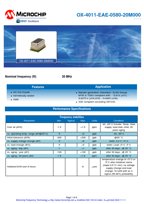
OX-4011-EAE-0580-20M000OCXONominal frequency (f0)20MHzFeaturesApplication•SC Cut Crystal •hermetically sealed •SMD•Wander generation (Standard /ZLAN Group)MTIE &TDEV compliant with:-G.812(zO1)-G.8273.4(zO4;zO5)-G.8263(zO6);•S3E compliant according GR1244Performance Specificationsall units in mmTP: max 260°C (@ solder joint, customer board level)T p: max: 10…30 secAdditional Information:This SMD oscillator has been designed for pick and place reflow solderingSMD oscillators must be on the top side of the PCB during the reflow process.Notes:Unless otherwise stated all values are valid after warm-up time and refer to typical conditions for supply voltage, frequency control voltage,load,temperature(25◦C).Subject to technical modification.USA:Europe:100Watts Street LandstrasseMt Holly Springs,P A1706574924NeckarbischofsheimGermanyTel:1.717.486.3411T el:+49(0)7268.801.0Fax:1.717.486.5920Fax:+49(0)7268.801.281Information contained in this publication regarding device applications and the like is provided only foryour convenience and may be superseded by updates.It is your reasonability to ensure that yourapplication meets with your specifications.MICROCHIP MAKES NO REPRESENT A TION ORWARRANTIES OF ANY KIND WHETHER EXPRESS OR IMPLIED,WRITTEN OR ORAL,ST ATUTORYOR OTHERWISE,RELA TED TO THE INFORMA TION INCLUDING,BUT NOT LIMITED TO ITSCONDITION,QUALITY,PERFORMANCE,MERCHANT ABILITY OR FITNESS FOR PURPOSE.Microchip disclaims all liability arising from this information and its e of Microchip devices in lifesupport and/or safety applications is entirely at the buyer’s risk,and the buyer agrees to defend,indemnify and hold harmless Microchip from any and all damages,claims,suits,or expenses resultingfrom such use.No licenses are conveyed,implicitly,or otherwise,under any Microchip intellectualproperty rights unless otherwise statedTrademarksThe Microchip and Vectron names and logos are registered trademarks of Microchip TechnologyIncorporated in the U.S.A.and other countries.List of appendicesAppendix_OX-4011-EAE-0580-20M000_Jitter II Appendix_OX-4011-EAE-0580-20M000_OX-401-9016-III 20M000_OX-4011-EAE-0580-10M000_MTIE_TDEVAppendix_OX-221-OX-40x_Power_on_time XIAppendix handling&processing note XIIThe following MTIE TDEV plots were generated from data collected on production devices over the course of a year and represent typical performance. Frequency is measured every second and converted to phase using Microchip’s golden standard TimeMonitor soft ware. Filtering is applied to the data per standards requirements, and limits where applicable, are shown in red. Additional information on standards and oscillatorrecommendations can be found in ZLAN-830 and ZLAN-3467 (formerly ZLAN-442 and ZLAN-68).Const. Temp ±1°K; slope 0,1°C/min, range 21..23°C Const. Temp ±5°F; slope 0,1°C/min,range 19.22..24.78°C Trapezoid_Pattern_slope 0,5°C/min,range +2,5...42,5°C Triangle-Pattern_slope 0,2°C/min,range -40...85°CConst. Temp ±1°K; slope 0,1°C/min, range 21..23°C Const. Temp ±5°F; slope 0,1°C/min,range 19.22..24.78°C Trapezoid_Pattern_slope 0,5°C/min,range +2,5...42,5°C Triangle-Pattern_slope 0,2°C/min,range -40...85°CConst. Temp ±1°K; slope 0,1°C/min, range 21..23°C Const. Temp ±5°F; slope 0,1°C/min,range 19.22..24.78°C Trapezoid_Pattern_slope 0,5°C/min,range +2,5...42,5°C Triangle-Pattern_slope 0,2°C/min,range -40...85°CConst. Temp ±1°K; slope 0,1°C/min, range 21..23°C Const. Temp ±5°F; slope 0,1°C/min,range 19.22..24.78°C Trapezoid_Pattern_slope 0,5°C/min,range +2,5...42,5°C Triangle-Pattern_slope 0,2°C/min,range -40...85°CConst. Temp ±1°K; slope 0,1, range 21..23°C Const. Temp ±5°F; slope 0,1,range 19.22..24.78°C Trapezoid_Pattern_slope 0,5,range +2,5...42,5°C Triangle-Pattern_slope 0,2,range -40...85°CConst. Temp ±1°K; slope 0,1, range 21..23°C Const. Temp ±5°F; slope 0,1,range 19.22..24.78°C Trapezoid_Pattern_slope 0,5,range +2,5...42,5°C Triangle-Pattern_slope 0,2,range -40...85°CConst. Temp ±1°K; slope 0,1, range 21..23°C Const. Temp ±5°F; slope 0,1,range 19.22..24.78°C Trapezoid_Pattern_slope 0,5,range +2,5...42,5°C Triangle-Pattern_slope 0,2,range -40...85°CConst. Temp ±1°K; slope 0,1, range 21..23°C Const. Temp ±5°F; slope 0,1,range 19.22..24.78°C Trapezoid_Pattern_slope 0,5,range +2,5...42,5°C Triangle-Pattern_slope 0,2,range -40...85°CApplicationUnless otherwise noted, the products listed in the catalogue are designed for use with ordinary electrical devices, such as stationary and portable communication, control, measurement equipment etc.. They are designed and manufactured to meet a high degree of reliability (lifetime more than 15 years) under normal …commercial“ application conditions. Products dedicated for automotive and H-Rel applications are specifically identified for these applications. If you intend to use these …commercial“ products for airborne, space or critical transport applications, nuclear power control, medical devices with a direct impact on human life, or other applications which require an exceptionally high degree of reliability or safety, please contact the manufacturer.Electrostatic SensitivityCrystal oscillators are electrostatic sensitive devices. Proper handling according to the established ESD handling rules as in IEC 61340-5-1 and EN 100015-1 is mandatory to avoid degradations of the oscillator performance due to damages of the internal circuitry by electrostatics. If not otherwise stated, our oscillators meet the requirements of the Human Body Model (HBM) according to JESD22-A114F.HandlingExcessive mechanical shocks during handling as well as manual and automatic assembly have to be avoided. If the oscillator was unintentionally dropped or otherwise subject to strong shocks, please verify that the electrical function is still within specification.Improper handling may also detoriate the coplanarity of bended leads of SMD components. SolderingOscillators can be processed using conventional soldering processes such as wave soldering, convection, infrared, and vapour phase reflow soldering under normal conditions. Solderability is guaranteed for one year storage under normal climatic conditions (+5°C to +35°C @ 40% to 75% relative humidity), however typically sufficient solderability –depending on the process – is maintained also for longer time periods. In cases of doubt, components older than one year should undergo a sample solderability test.The recommended reflow solder profile for SMT componets is according IPC/JEDEC J-STD-020 (latest revision)SMD oscillators must be on the top side of the PCB during the reflow process.After reflow soldering the frequency of the products may have shifted several ppm, which relaxes after several hours or days, depending on the products. For details please contact the manufacturer.CleaningCleaning is only allowed for hermetically sealed oscillators. Devices with non hermetical enclosures (e.g. with trimmer holes) shall not be cleaned by soaking or in vapour, because residues from the cleaning process may penetrate into the interior, and degrade the performance.Our products are laser marked. The marking of our oscillators is resistant to usual solvents, such as given in IEC 60068-2-45 Test XA. For applicable test conditions see IEC 60679-1.Ultrasonic cleaning is usually not harmful to oscillators at ultrasonic frequencies of 20kHz at the sound intensities conventional in industry. Sensitive devices may suffer mechanical damage if subjected to 40kHz ultrasound at high sound pressure. In cases of doubt, please conduct tests under practical conditions with the oscillators mounted on the PC board.Hermetical SealIf the device is specified as hermetically sealed, it meets the requirements of IEC 60679-1, i.e. for enclosures with a volume smaller than 4000mm³ the leak rate is below 5*10-8 bar cm3/s, for larger enclosures it is below 1*10-6 bar c bar cm3/s, tested according to IEC 60068-2-17 Test Qk.Glass feed-throughs may be damaged as a result of mechanical overload, such as bending the connection leads or cutting them with an unappropriated tool. In order to avoid microcracking, the wire must be held fixed in position by a pressure pad between glass feed-through and the bending point during the bending process. Check: there should be no damaged edges on the glass feed-through after the bending.Tape & ReelThe packing in tape and reel is according to IEC 60286-3.Details see tape & reel data sheets.QualificationVectron products are undergoing regular qualification/reliability tests as per product family definition. Results are available upon request. Customer specific qualification tests are subject to agreement.If not otherwise stated, the product qualifications are performed according to IEC 60679-5 or other valid industry standards.ScreeningOur oscillators are 100% tested, and all key manufacturing processes are controlled by Statistical Process Control (SPC). Additional screening is therefore usually not required.On request, we can perform screening tests according to MIL-PRF-55310, class B for discrete or hybrid constructions of commercial (COTS) products. For special requirements see the High Reliability Clock section.Demounting/Desoldering of Ocsillator device for analysis:The removal or desoldering of oscillators from customer application after SMT process may cause damage to the device if not handeld appropriately. It may lead to parametric change such as frequency shift (like OCXO: up to +/- 200 ppb) . It is utmost important to minimize the direct heat exposure to the device in order to avoid such effects. Use of hot air gun for desoldering should be avoided.A mechanical stress could also destroy the part, if exposed to excessive mechanical shock after removal process. Appropriate shock protection & ESD designated packaging must be used to avoid any external mechanical shock for FA return process.In general, the products* withstand the tests listed in the following Table 1, which are based on valid industry standards.*Additional note: Test conditions could vary for different product families and individual product specifications depending on the customer as well as product requirements.Recommended Environmental Test ConditionsTable 1。
晶振选型的参数

晶振选型的参数1.、频率大小:频率越高一般价格越高。
但频率越高,频差越大,从综合角度考虑,一般工程师会选用频率低但稳定的晶振,自己做倍频电路。
总之频率的选择是根据需要选择,并不是频率越大就越好。
要看具体需求。
比如基站中一般用10MHz的恒温晶振(OCXO),因其有很好的频率稳定性,属于高端晶振。
至于范围,晶振的频率做的太高的话,就会失去意义,因为有其他更好的频率产品代替。
JFVNY的产品频率范围是:25kHz-1.3G,基本上所有应用中的晶振都可以在JFVNY产品种找到。
2.、频率稳定度:关键参数,JFVNY的高端晶振可以达到10-9级别。
指在规定的工作温度范围内,与标称频率允许的偏差,用PPm (百万分之一)表示。
一般来说,稳定度越高或温度范围越宽,价格越高。
对于频率稳定度要求±20ppm或以上的应用,可使用普通无补偿的晶体振荡器。
对于介于±1 至±20ppm 的稳定度,应该考虑温补晶振TCXO 。
对于低于±1ppm 的稳定度,应该考虑恒温晶振OCXO。
如果客户有十分特别的频稳要求,JFVNY可根据客户要求参数定做。
2、电源电压:常用的有1.8V、2.5V、3.3V、5V等,其中3.3V应用最广。
3、输出:根据需要采用不同输出。
(HCMOS,SINE,TTL,PECL,LVPECL,LVDS,LVHCMOS等)每种输出类型都有它的独特波形特性和用途。
应该关注三态或互补输出的要求。
对称性、上升和下降时间以及逻辑电平对某些应用来说也要作出规定,根据客户需要我们可以帮助客户选型。
5.、工作温度范围:工业级标准规定的-40~+85℃这个范围往往只是出于设计者们的习惯,倘若-20℃~+70℃已经够用,那么就不必去追求更宽的温度范围。
对于某些特殊场合如航天军用等,对温度有更苛刻的要求。
6.、相位噪声和抖动:相位噪声和抖动是对同一种现象的两种不同的定量方式,是对短期稳定度的真实度量。
晶振选型与应用知识
石英晶振选型与应用知识石英晶体是压电晶体的一种,沿着特定的方向挤压或拉伸,它的两端会产生正负电荷,这种效应称为正压电效应;相反,对晶体施加电场导致晶体形变的效应,称为逆压电效应。
所以在石英晶片两面施加交变电场,晶片就会产生形变,而形变又会产生电场,这是一个周期转换的过程。
对于特定的晶片,这个周期是固定的,我们利用这个周期来产生稳定的基准时钟信号。
石英晶体元器件,是利用石英晶体的压电效应实现频率控制、稳定或选择的关键电子元器件。
包括石英晶体谐振器、石英晶体振荡器和石英晶体滤波器。
在石英晶片的两面镀上电极,经过装架、调频、封装等工序后制成石英晶体元件。
石英晶体元件与集成电路等其它电子元件组合成石英晶体器件。
本文主要介绍石英晶振:即所谓石英晶体谐振器(无源晶振)和石英晶体振荡器(有源晶振)的统称。
一般的概念中把晶振就等同于谐振器理解了,振荡器就是通常所指钟振。
石英晶振是一种用于稳定频率和选择频率的电子元件,已被广泛地使用在无线电话、载波通讯、广播电视、卫星通讯、仪器仪表等各种电子设备中.一、石英晶振的型号命名方法1.国产石英晶体谐振器的型号由三部分组成:–第一部分:表示外壳形状和材料,B表示玻璃壳,J表示金属壳,S表示塑料封型;–第二部分:表示晶片切型,与切型符号的第一个字母相同,A表示AT切型、B表示BT切型,–第三部分:表示主要性能及外形尺寸等,一般用数字表示,也有最后再加英文字母的。
JA5为金属壳AT切型晶振元件,BA3为玻壳AT切型晶振元件。
2石英晶体振荡器的型号命名有四部分组成:.–第一部分:主称用大写字母Z表示石英晶体振荡器;–第二部:类别用大写字母表示,其意义见下表:–第三部分:频率稳定度等级用大写字母表示,其意义见下表:–第四部分:序号用数字表示,以示产品结构性能参数的区别从型号上无法知道晶振元件的主要电特性,需查产品手册或相关资料才行。
二、石英晶振的结构特点1.石英晶体谐振器一般由外壳、晶片、支架(金属座)、外引线、引线等组成。
epson晶振选型手册
Epson晶振选型手册引言概述:Epson晶振选型手册是一本提供关于Epson晶振选型的专业指导手册。
晶振作为一种重要的电子钟振装置,广泛应用于各类电子设备中,对于设备的稳定性和精准性起到关键作用。
本手册将从多个方面介绍Epson晶振的选型原则和方法,以帮助读者准确选型和应用。
正文内容:1. 晶振的基本原理1.1 晶振的作用与功能1.1.1 提供时钟信号1.1.2 稳定电子设备的工作频率1.1.3 控制和同步各设备之间的通信1.1.4 精确计时和定时功能1.2 晶振的工作原理1.2.1 晶体振荡原理1.2.2 纯谐振条件与频率稳定性1.2.3 晶振的构造与材料选择2. Epson晶振的特点与优势2.1 高稳定性和低功耗2.1.1 稳定性与频率偏移2.1.2 低功耗对电池寿命的影响2.2 宽温度范围和长寿命2.2.1 温度对晶振频率的影响2.2.2 长期使用的可靠性和稳定性2.3 大容量和小封装尺寸2.3.1 容量对数据传输速率的影响2.3.2 封装尺寸对电路板设计的要求3. Epson晶振选型原则3.1 需求分析和参数确定3.1.1 设备类型和用途3.1.2 工作频率和精度要求3.1.3 温度范围和环境影响3.2 选择适合的晶振类型3.2.1 晶振频率范围和精度等级3.2.2 温度补偿和温度响应特性3.2.3 封装尺寸和安装要求3.3 参考设计和测试验证3.3.1 参考电路设计3.3.2 振荡电路测试和频率测量3.3.3 选型结果评估和优化4. Epson晶振选型案例分析4.1 移动方式晶振选型4.1.1 高稳定性和小封装尺寸的需求4.1.2 多频段应用的选择考虑4.2 电子表计晶振选型4.2.1 长期使用和温度范围要求4.2.2 低功耗和电池寿命的平衡4.3 工业自动化控制晶振选型4.3.1 高频率和精度要求4.3.2 多通道同步和控制4.3.3 长寿命和可靠性的考虑5. Epson晶振应用注意事项5.1 环境温度和封装要求5.2 抗振动和抗干扰性能5.3 防静电措施和电源干扰5.4 长期使用和老化问题结语:本手册全面介绍了Epson晶振的选型原则和方法,包括晶振的基本原理、Epson晶振的特点与优势、选型原则、案例分析以及应用注意事项。
大普晶振的选型
晶振的等级
DAPU
如何确定频率准确度
影响频率准确度的主要因素 出厂准确度 + 温度漂移 + 电压特性 + 负载特性 + 老化漂移
DAPU 案例:
假如一台仪器在实验室使用,采用10.00MHz作为基准时钟,对时钟提出的频率稳 定度为 10年内频率最大不超过0.5PPM,即为5Hz
选型推荐: 出厂准确度 :8E-8 温度稳定度:5E-9 @-30至70度 电压特性:2E-9 负载特性:2E-9 老化率:5E-8/year, 4E-7/10year 此时钟 10年频率漂移为 4.89Hz ,符合选型要求
波形的选择
波形的选择主要取决于设备时钟芯片的要求和现有晶振产品的限制:
波形
优点
缺点
产品类型
DAPU 削顶正弦波
HCMOS/TTL
谐波干扰小、 体积小
驱动能力强
驱动能力弱 谐波干扰大
SMD‐7050、5032、 3225
OSC\VCXO\OCXO、 TCXO
标准正弦波 谐波干扰极小 电路复杂
OCXO、TCXO
O54, 50x40x12.7
O55, 50x50x12.7
TCXO 行业主要标准尺寸
尺寸的选择
DAPU T10A, 12.7*12.7*6
T11A, 20.7*12.7*8
M11A 20*12.7*10
M21B 25*15*10
T3225 3.2*2.5*1.5
T53 5*3.2*1.5
T75 7*5*2
广东省大普通信技术有限公司
DAPU
DAPU Telecom
目录
1
晶振选型的要点
2 晶振的等级
爱普生 EPSON 有源贴片晶振 SG7050CAN 12.288000MHz 规格参数、数据手册、规格书信息
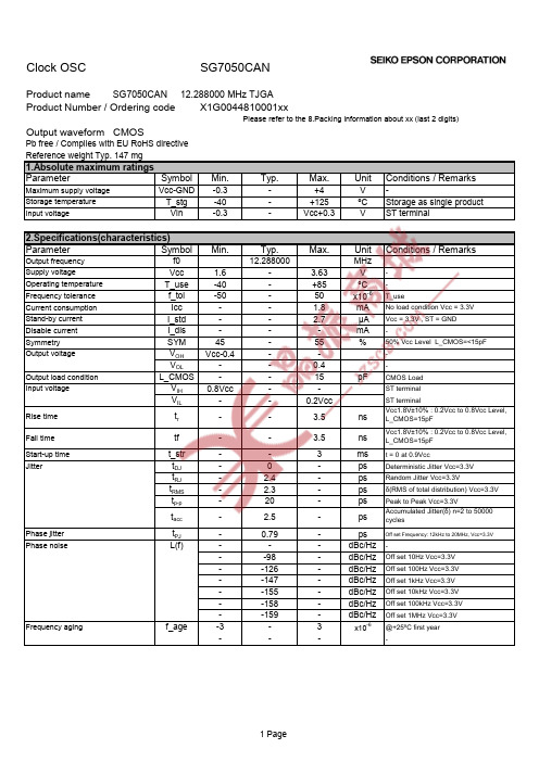
Clock OSC SG7050CANProduct nameSG7050CAN 12.288000 MHz TJGA Product Number / Ordering code X1G0044810001xxPlease refer to the 8.Packing information about xx (last 2 digits)Output waveform CMOSPb free / Complies with EU RoHS directiveReference weight Typ. 147 mg1.Absolute maximum ratings Parameter SymbolMin.Typ.Max.UnitConditions / RemarksMaximum supply voltage Vcc-GND -0.3-+4V -Storage temperature T_stg -40-+125ºC Storage as single product Input voltageVin-0.3-Vcc+0.3VST terminal2.Specifications(characteristics)Parameter SymbolMin.Typ.Max.UnitConditions / RemarksOutput frequency f012.288000MHz Supply voltage Vcc 1.6- 3.63V -Operating temperature T_use -40-+85ºC -Frequency tolerance f_tol -50-50x10-6T_useCurrent consumption Icc -- 1.8mA No load condition Vcc = 3.3V Stand-by current I_std -- 2.7 µA Vcc = 3.3V , ST = GND Disable current I_dis ---mA -Symmetry SYM 45-55%50% Vcc Level L_CMOS=<15pF Output voltage V OH Vcc-0.4---V OL --0.4-Output load condition L_CMOS --15pFCMOS Load Input voltageV IH 0.8Vcc --ST terminalV IL--0.2Vcc ST terminalRise time t r -- 3.5ns Fall time tf -- 3.5ns Start-up time t_str --3ms t = 0 at 0.9VccJittert DJ -0-ps Deterministic Jitter Vcc=3.3V t RJ - 2.4-ps Random Jitter Vcc=3.3Vt RMS - 2.3-ps δ(RMS of total distribution) Vcc=3.3V t p-p -20-ps Peak to Peak Vcc=3.3Vt acc- 2.5-ps Phase jitter t PJ -0.79-ps Off set Frequency: 12kHz to 20MHz, Vcc=3.3VPhase noise L(f)---dBc/Hz ---98-dBc/Hz Off set 10Hz Vcc=3.3V --126-dBc/Hz Off set 100Hz Vcc=3.3V --147-dBc/Hz Off set 1kHz Vcc=3.3V --155-dBc/Hz Off set 10kHz Vcc=3.3V --158-dBc/Hz Off set 100kHz Vcc=3.3V --159-dBc/HzOff set 1MHz Vcc=3.3V Frequency aging f_age-3-3x10⁻⁶@+25ºC first year ----Vcc1.8V±10% : 0.2Vcc to 0.8Vcc Level,L_CMOS=15pFVcc1.8V±10% : 0.2Vcc to 0.8Vcc Level,L_CMOS=15pF Accumulated Jitter(δ) n=2 to 50000cycles3.Timing chart4.Test circuit1) Waveform observation2) Current consumption*Current consumption under the disable function should be = GND.3) Condition (1) Oscilloscope· Band width should be minimum 5 times higher (wider) than measurement frequency.· Probe earth should be placed closely from test point and lead length should be as short as possible * Recommendable to use miniature socket. (Don’t use earth lead.)(2) L_CMOS also includes probe capacitance.(3) By-pass capacitor (0.01 µF to 0.1 µF) is placed closely between VCC and GND.(4) Use the current meter whose internal impedance value is small.(5) Power supply· Start up time (0 %VCC to 90 %VCC) of power source should be more than 150 µs.· Impedance of power supply should be as lowest as possible.GNDV CC tr 50 %V CCttw80 %V CC20 %V CC tfV CCSTOUTGNDswichsupplyby-pass capacitorTest PointAor OEor OEV CCSTOUTGNDsupplyby-pass capacitorL_CMOSTest Point5.External dimensions (Unit: mm)6.Footprint(Recommended) (Unit: mm)7.Reflow profileReflow condition (Follow of JEDEC STD-020D.1)8.Packing information[ 1 ]Product number last 2 digits code(xx) descriptionThe recommended code is "00"X1G0044810001xxCode Code 01Any Q'ty vinyl bag(Tape cut)13500pcs / Reel 11Any Q'ty / Reel 001000pcs / Reel12250pcs / ReelConditionCondition Note.OE pin = "H" or "open" : Specified frequency output. OE pin = "L" : Output is high impedance.ST pin = "H" or "open" : Specified frequency output.ST pin = "L" : Output is high impedance 、oscillation stops.#2CC (ex. 0.01 µF)1.8 5.084.22.0#1#3#4Resist1.3±0.25.0±0.27.0±0.2#4 #1#3#2E 25.000CAN395K1.41.1C0.55.08Temperature [ ºC]6030025020015010050Time [ s ]120180240300360420480540600660720780Ts min: +150 ºCTs max: +200ºCTL: +217ºC+255ºCtp: at least 30 sTP: +260ºC OVERTime: +25 ºC to PeakRamp-up rate +3 ºC/s Max.tL60 s to 150 s( +217 ºC over )ts60 s to 120 s( +150ºC to +200ºC)Ramp-down rate -6 ºC/s Max.[ 2 ] Taping specificationSubject to EIA-481 & IEC-60286(1) Tape dimensions Material of the Carrier Tape : PS Material of the Top Tape : PET+PEUnit: mmSymbol A B C D E F Valueφ1.5489.25162.3(2) Reel dimensionsCenter material : PS Material of the Reel : PSA BDECFTop tapeCarrier tapeEPSONEPSONUser direction of feed9.Notice10.Contact us· This material is subject to change without notice.· Any part of this material may not be reproduced or duplicated in any form or any means without the written permission of Seiko Epson.· The information about applied data,circuitry, software, usage, etc. written in this material is intended for reference only.Seiko Epson does not assume any liability for the occurrence of customer damage or infringing on any patent or copyright of a third party.This material does not authorize the licensing for any patent or intellectual copyrights.· When exporting the products or technology described in this material, you should comply with the applicable export control laws and regulations and follow the procedures required by such laws and regulations.· You are requested not to use the products (and any technical information furnished, if any) for the development and/or manufacture of weapon of mass destruction or for other military purposes. You are also requested that youwould not make the products available to any third party who may use the products for such prohibited purposes.· These products are intended for general use in electronic equipment. When using them in specific applications that requireextremely high reliability, such as the applications stated below, you must obtain permission from Seiko Epson in advance./ Space equipment (artificial satellites, rockets, etc.)/ Transportation vehicles and related (automobiles, aircraft, trains, vessels, etc.) / Medical instruments to sustain life / Submarine transmitters / Power stations and related/ Fire work equipment and security equipment / Traffic control equipment/ And others requiring equivalent reliability.。
- 1、下载文档前请自行甄别文档内容的完整性,平台不提供额外的编辑、内容补充、找答案等附加服务。
- 2、"仅部分预览"的文档,不可在线预览部分如存在完整性等问题,可反馈申请退款(可完整预览的文档不适用该条件!)。
- 3、如文档侵犯您的权益,请联系客服反馈,我们会尽快为您处理(人工客服工作时间:9:00-18:30)。
ISO 14000 是国际标准化组织于 1996 年在全球化变暖、 臭 氧层破坏、以及全球毁林等环境问题日益严重的背景下提 出的环境管理国际标准。
追求高品质
Seiko Epson 为了向顾客提供高品质、卓越信赖性的产品、服务,迅 速着手通过 ISO 9000 系列资格认证的工作,其日本和海外工厂也在通 过 ISO 9001 认证。 同时, 也在通过大型汽车制造厂商要求规格的 ISO/TS 16949 认证。 ISO/TS16949 是一项国际标准,是在 ISO9001 的基础上增 加了对汽车工业的特殊要求部分。
规格(特征)
项目
额定频率范围 储存温度范围 工作温度范围 激励功率 频率公差 频率温度特征 负载电容 串联电阻(ESR) 频率老化
符号
f_nom T_stg T_use DL f_tol f_tem CL R1 f_age
规格说明 用于为汽车
12.000 MHz ~ 60.000 MHz -40 C ~ +125 C -40 C ~ +125 C 200 W Max. 15 10 ~ 50 10
【领先的片式无源器件整合供应商—南京南山半导体有限公司】
推进环境管理体系 符合国际标准
在环境管理体系的运行方面,使用 ISO14001 国际环境标准,通过“计 划-实施-检查-验证(PDCA)的循环来实现持续改进。公司位于日本和 海外的主要制造基地已取得了 ISO14001 资格认证。
-6
7 pF ~ 如下表所示 5 10 / year Max.
-6
串联电阻(ESR)
频率
12.0 MHz f_nom 13.0 MHz 13.0 MHz < f_nom < 20.0 MHz 20.0 MHz f_nom < 25.0 MHz 25.0 MHz f_nom 60.0 MHz 产品名称 (标准显示)
关于在目录内使用的记号
●无铅。 ●符合欧盟 RoHS 指令。 欧盟 RoHS 指令免检的含铅产品。 (密封玻璃、高温熔化性焊料或其他材料中包含铅。 ) ●为汽车方面的应用,如汽车多媒体、车身电子、遥控无钥门锁等。
●为汽车行驶安全方面的应用(引擎控制单元、气囊、电子稳定程序控制系统) 。
注意事项
·本材料如有变更,恕不另行通知。量产设计时请确认最新信息。 ·未经 Seiko Epson 公司书面授权,禁止以任何形式或任何方式复制或者发布本材料中任何部分的信息内容。 ·本材料中的书面信息、应用电路、编程、使用等内容仅供参考。Seiko Epson 公司对第三方专利或版权的侵权行为不负有任何责任。本材料 未对任何专利或知识版权的许可权进行授权。 ·本材料中规格表中的数值大小通过数值线上的大小关系表示。 ·当出口此材料中描述的产品或技术时,你应该遵守相应的出口管制法律和法规,并按照这些法律和法规的要求执行。 请不要将产品(以及任何情况下提供任何的技术信息)用于开发或制造大规模杀伤性武器或其他军事用途。还要求,不要将产品提供给任何 将产品用于此类违禁用途的第三方。 ·此类产品是基于在一般电子机械内使用而设计开发的,如将产品应用于需要极高可靠性的特定用途,必须实现得到弊公司的事前许可。若 无许可弊公司将不负任何责任。 1.太空设备(人造卫星、火箭等) 2.运输车辆机器控制装置(汽车、飞机、火车、船舶等) 3.用于维持生命的医疗器械 4.海底中转设备 5.发电站控制机器 6.防灾防盗装置 7.交通设备 8.其他,用于与 1~7 具有同等可靠性的用途。
本材料中记载的品牌名称或产品名称是其所有人的商标或注册商标。
Seiko Epson Corporation
外部尺寸规格
推荐焊盘尺寸
(单位:mm)
#4
#3
2000P e39RA
#1 3.2±0.1
2.5±0.1
2.2
#2 0.7 Max.
1.6
1.2 #1 #2 #4 0.7 C 0.3 Min. #1
内部连接 (TOP VIEW)
#3 #2 1.4
1.2
#4
0.8
0.9
#3
#2 和 #4 连接到外壳。 (请接地)
串联电阻
120 Max. 80 Max. 60 Max. 50 Max.
FA-238A 28.636360kHz 18.0 +15.0-15.0 ① ② ③ ④ -6 ①型号 ②频率 ③负载电容(pF) ④频率稳定度(× 10 ,+25 C) 如果咨询的话,请注明频率温度特性和工作温度范围 (单位: mm)
-6 -6 -6
Hale Waihona Puke 条件基频 请联系我们以便获取其它可用频率的相关信息 裸存 推荐: 1 W ~ 100 W +25 C 请联系我们以便获取相关信息 请联系我们以便获取相关信息 可指定 -40 C ~ +125 C, DL=100 W +25 C, 第一年
30 10 / -40 C ~ +85 C 50 10 / -40 C ~ +125 C
授权代理商
领先的片式无源器件整合供应商
www.nscn.com.cn
E_mail:nj@nscn.com.cn
晶体单元
产品号码(请联系我们) X1E000341xxxx00
MHz 频率范晶体单元 车载用
FA - 238A
额定频率范围 外部尺寸规格 谐波次数 应用 依据 AEC-Q200 : : : : 12 MHz ~ 60 MHz 3.2× 2.5×0.7 mm 基频 汽车音响, ECU 时钟, 时钟, 汽车导航系统, 仪表, 遥控无匙门禁 实际尺寸