对讲机原理图
对讲机天线制作原理图

对讲机天线制作原理图
对讲机天线的制作原理图如下:
1. 选择合适的导体材料,如铜线或铝线。
2. 将导体材料按照天线的长度要求进行剪裁,通常为1/4或
1/2波长。
3. 在导体的一端剥开绝缘层,露出内部的金属。
4. 将导体连接到对讲机的天线接头上,确保稳固的连接。
5. 检查天线的形状和长度,确保与设计要求相符。
6. 使用导线夹或其他固定装置将天线固定在合适的位置上。
7. 调整天线的方向和位置,以获得最佳的信号接收和发射效果。
请注意,以上只是对讲机天线制作的一般原理图,具体的制作过程可能因对讲机型号和材料的不同而有所差异。
半双工调频无线对讲机

半双工调频无线对讲机一、实验目的1、在模块实验的基础上掌握调频发射机、接收机,整机组成原理,建立调频系统概念。
2、掌握系统联调的方法,培养解决实际问题的能力。
二、实验内容•完成调频发射机整机联调。
•完成调频接收机整机联调。
•进行调频发送与接收系统联调。
三、实验仪器1、高频实验箱 2台2、双踪示波器 1台四、实验原理半双工是指接收与发送共用一个载波信道,但同一时刻只能发送或只能接收的传输方式,半双工调频对讲机组成原理框图发射机由音源,音频放大,调频、上变频、高频功放等电路组成。
接收机则由高放,下变频、中频放大、鉴频、音频功放、耳机等部分组成。
发送与接收频率同为10.7M,公用一根天线。
收发的切换依靠10号板的J1完成.J1在没有按下去的情况下为接收状态,按下去为发送。
为了避免自身的发送对接收的干扰,所以加入了电源控制。
电源控制的作用是当接收电路工作时,发送电路关闭,反之亦然。
调频发射机的工作原理是:音源经音频放大进行调频(LC调频振荡器产生频率f0=4.5MHZ的中频振荡,变容二极管线性调频)后输出FM信号f1(最大频偏Δf m=±20KHZ,整个发射机的频率稳定度由该级决定);进入混频级,本机振荡器输出的另一高频信号f2(6.2MHZ)亦进入混频级,则混频级的输出为含有f1、f2、(f1+f2)、(f2-f1)等频率分量的信号;混频级的输出接调谐回路选出高频信号(f2+f1),经功率激励级放大的信号进入末级功放进行功率放大,使负载(天线)上获得满足要求的发射功率。
如果要求整机功率较高,如要求ηA>50%,应采用丙类功率放大器。
调频发射机的主要技术指标有:1.发射功率发射功率PA一般是指发射机输送到天线上的功率。
只有当天线的长度与发射机高频振荡的波长λ相比拟时,天线才能有效地把载波发射出去。
若接收机的灵敏度UA=2μV,则通信距离s与发射功率PA的关系为2.工作频率或波段发射机的工作频率应根据调制方式,在国家或有关部门所规定的范围内选取。
无线调频对讲机

无线调频对讲机一、无线对讲机无线对讲机作为一种简单的通信工具,由于它不需要中转和地面交换机站支持,就可以进行移动通信。
所以深受人们欢迎。
目前广泛应用于生产、保安、野外工程等领域的小范围通信工程中。
无线对讲机技术是很多无线移动通信技术的基础,目前应用较广泛的蜂窝式移动电话技术,就是在无线双工对讲机的基础上,发展起来的新兴现代通信技术。
很好的熟悉掌握无线对讲机内部电路的工作原理和测试、调整技术,对今后从通信工程领域的技术工作,无疑是十分重要的。
对讲机的电路形式较多,从调制方式上可分为调幅式和调频式,从收发功能上,可分为单工式和双工式。
单工式对讲机同一时间内,只能工作在一种状态下,即:接收或者发射状态。
而事不能同时处于收发状态,单工对讲机工作时,要不停的切换开关来控制收发状态。
而双工式对讲机,可以收发电路同时工作,使用起来如同普通电话机一样,应用起来比较方便,但由于双工对讲机电路复杂,造价高,耗电量大等缺点,所以应用较少。
而单工式对讲机,则由于它造价低,体积小,耗电低等优点,被大量应用。
目前市面上常见到的对讲机大多属于单工调频式。
图1-1就是单工式对讲机的原理框图:图1-1 无线对讲机电路原理框图从图中所看出,对讲机的收、发状态,是靠切换供电电源的方式,来实现收发转换的,虽然电路中含有接收和发射电路,由于在同一时间内,只能工作在一种状态下,所以将这种工作方式称为单工方式。
本设计主要是针对蛋工对讲机进行的,将对单工调频对讲机电路各部分电路进行详细的分析,图1-2是本设计用的单工无线调频对讲机电路方框图:图1-2 单工无线对讲机电路方框图二、系统设计1.设计要求:(1)任务设计并制作一个单工调频对讲机,实现甲乙两点之间的单工语音传输业务。
(2)要求:a.设计并制作对讲机的发射单元,其发射频率在30MHZ左右,发射功率大于1W(在75Ω无线上测定),调制方式为调频,最大调制频偏≥±3kHz。
b. 设计并制作对讲机的接收单元,其接收频率与发射频率相同,接收灵敏度≤5uV,音频输出功率50mw。
高等教育:对讲机原理介绍

2019/12/17
Copyright by penghx from
13
2019/12/17
Copyright by penghx from
14
1.2 超外差方式原理
1.2.3 超外差接收机
从天线接收的信号经高频放大器(见调谐放大器)放 大,与本地振荡器产生的信号一起加入混频器变频, 得到中频信号,再经中频放大、检波和低频放大,然 后送给用户。
3 调频对讲机的安装与调试
元件测试与安装 调试与维修过程
Copyright by penghx from
2
1 对讲机原理相关知识
2019/12/17
Copyright by penghx from
3
1.1 无线通信概述
1.1.1 声波
2019/12/17
Copyright by penghx from
18
1.2 超外差方式原理
缺点与解决办法
电路比较复杂; 存在着一些特殊的干扰,如像频干扰、组合频率干扰和中频
干扰等。
解决途径 提高高频放大器的选择性,尽量把由天线接收到的像频干扰
信号滤掉; 另一种办法是采用二次变频方式。
2019/12/17
Copyright by penghx from
19
1.2 超外差方式原理
1.2.4 二次变频超外差接收机
第一中频频率选得较高,使像频干扰信号的中心频率 与有用输入信号uc的中心频率差别较大,使像频信号 在高频放大器中受到显著的衰减。
第二中频频率选得较低,使第二中频放大器有较高的 增益和较好的选择性。
后来广泛采用的是超外差接收机,主要依靠频率固定的 中频放大器放大信号。
公众对讲机原理图

ATLANTIC-I Ricetrasmettitore marino portatile Handheld marine transceiverCod.603774 Via R. Sevardi42010 Reggio Emilia – Italywww.cte.itA). GENERAL DESCRIPTIONThe Atlantic Marine radio is a self-contained transceiver unit with integral antenna intended for use as a general communication tool. The useable range, while dependent upon terrain and other radio propagation principles, is typically five miles. The Atlantic uses the maximum transmit power allowed to help ensure the maximum communication range.Features include: Channels, 10 channels Weather radio, Channel Monitor, Page and LCD Display. The unit is equipped with an external Headset option connector. Four AA alkaline batteries that are readily available in retail outlets supply operating power. An automatic power savings feature allows the typical standby battery life to extend to more than 10 days. B). FREQUENCY DETERMINING CIRCUITSThe fundamental frequency for both the transmitter and the receiver local oscillators are controlled by a phase lock loop (PLL) circuit IC201 (Toshiba TB31202, or equipvalent). The frequency of operation of the FRS voltage controlled oscillator (VCO), composed of Q301 and Q302 operating in cascade is phase locked to a voltage controlled crystal reference (VCXO) operating at 20.95MHz (X202).The VCO is locked to the fundamental of the transmit signal in the transmit mode and is locked to the receive 1st LO (Fundamental channel frequency minus 21.4MHz) in the receive mode. The crystal reference frequency is shared with the 2nd LO of 20.95MHz.C). TRANSMITTER CIRCUITSThe transmitter amplifies the 0 dBm signal from the VCO to approximately 27dBm that is fed to the antenna. The transmitter is a three stage amplifier composed of Q1,3,4 and Q11. The first two stages are operated class A and the final is operated class B in full saturation to help prevent unwanted amplitude modulation. The fundamental transmit signal is fed through an elliptical low pass filter (5-pole, 2 zero) in order to suppress the harmonics to below –50 dBc. The desired frequency modulation of the carrier is accomplished by modulating the current in the VCO directly with the microphone audio signal. The microphone audio is conditioned with a three-pole high pass filter at 300 Hz (IC5C,D), a hard clipper circuit (IC5B) to limit maximum deviation to +/- 2.5 kHz and a three-pole low pass or splatter filter at 2.8 kHz (IC5AD). RECEIVER CIRCUITSThe received signal from the antenna is band limited to 200Mhz by the transmitter harmonic filter. The desired signal is fed to a low noise amplifier (LNA – Q6) centered from 156MHz to 164MHz that provides approximately 10 dB of gain. The output of the LNA is filtered with a Band Pass filter (SF1) with pass-band of 156 to 164MHz and stopband attenuation of 50 dB. The filtered receive signal is one input to the 1st mixer (Q8), the other mixer input (1st LO) is the output of the VCO at the desired channel frequency minus 21.4MHz. The output of the mixer is tuned to the 1st IF of 21.4 MHz.The 1st IF is transformer coupled for impedance matching to a X-tal filter centered at 21.4MHz with a bandwidth of +/-3.75Hz. The filtered 1st IF is then amplified by Q9 and fed to the 2nd mixer input of the multi-function receiver IC (IC1). The 2nd LO (20.95 MHz) is generated by VCXO that is the reference frequency for the PLL. The 2nd mixer output of 450 kHz is filtered through a 4 section ceramic filter that in combination with the 21.4MHz X-tal filter provides approximately 50 dB of adjacent channel attenuation. The 450 kHz 2nd IF is then amplified, limited and fed to a quadrature detector for FM demodulation. The resulting audio output signal is bandpass filtered from 300 to 3 kHz (Q22) and amplified to provide 150mW of audio power (IC2). A squelch circuit is provided (IC1 pins 10 through 11) to mute the receiver noise under low signal conditions. The squelch circuit amplifies and detects noise in a narrow bandwidth at approximately 5 kHz. When the detected noise exceeds a threshold set to trigger at approximately 9 dB SINAD receive signal strength, the audio output is muted.E). TRANSMIT/RECEIVE SWITCHWhen the radio is in the transmit mode, pin diode switches D13 and D1 are both turned on (representing less than 0.7 ohms). D13 allows the transmit signal to pass to the antenna and D1 shorts one leg of a T matching network (L3, L15 and C4) to ground in the receive path. This results in a parallel tuned circuit high impedance being presented to the transmit signal so that the receive path does not load the transmit signal. In the receive mode, both D13 and D1 are off, resulting in the antenna signal being coupled into the receive LNA through the 50 ohm T matching network and the unwanted load of the transmit final amplifier is reduced to less than 1 pF by D1.F). RADIO CONTROL CIRCUITA microprocessor (CPU1) is used to control the transceiver. User stimuli is provided through a tack switch for PTT (push to talk), along with the keypad for channel selection, channel monitor, receive volume, and page. Pressing the PTT switch instructs CPU1 to switch to the transmit mode. This is accomplished by loading the proper channel counter information through a 3-wire serial link to the PLL IC (IC201), turning on power to the PLL and VCO, microphone and transmit audio circuits and the transmit RF amplifiers.Pressing the call switch causes the microcontroller to transmit a warbling tone for approximately 3 seconds on the current channel selected that is used to notify another person with Marine radio that you wish to communicate. Pressing the channel Up/Down buttons (active in receive mode only) instructs CPU1 to increment or decrement respectively the channel frequency by one channel from the channel previously selected.In receive mode the microcontroller periodically switches on the VCO and receiver power and checks for a valid received signal by monitoring the squelch circuit output. If a valid signal is present, the audio output is turned on and receive power is maintained for the duration of the valid signal. If the valid signal is removed or no valid signal was present, the microcontroller removes power from the VCO and receiver, waits for approximately 100 ms and then checks again. This periodic cycling of the power to the receiver circuits results in a much longer battery life vs. leaving power on continuously. The total period of the cycling is selected such that the worst case delay in ‘seeing’ a valid receive signal is not disruptive to normal two-way voice communications.Midland ATLANTIC-I Test and Alignment ProcedureREVISION SHEETRev. Code Rev. Date Revision Revised By:TABLE OF CONTENT1. RECOMMENDED EQUIPMENT (4)2. TEST PREPARATION (4)3. CRYSTAL SELECT (4)4. VCO ADJUSTMENT (4)5. TRANSMITTER FREQUENCY ALIGNMENT (5)6. TRANSMITTER OUTPUT POWER CHECK (5)7. TRANSMITTER DEVIATION ADJUSTMENT (5)8. RECEIVER ALIGNMENT (6)9. SQUELCH THRESHOLD AND HYSTERISIS (6)10. VOX TEST (6)11. LOW BATTERY LEVEL TEST (6)12. CHARGING TEST (6)1. RECOMMENDED TEST EQUIPMENT1.1 HP8920A,B Radio Communication Tester or equivalent1.2 Fluke 187 Digital Voltmeter or equivalent1.3 HPE3615A Power Supply or equivalent2. TEST PREPARATION2.1 Connect a 6.0Vdc power supply to the positive battery terminal input point and thenegative battery terminal input point (GND) into the negative terminal.2.3 Connect the HP8920A,B RF Output port to the ANT point.2.4 TP12 should be connected to the Audio In Hi and Spkr (-) should be connected tothe GND of the HP8920B.2.5 Set the unit at Ch1.3. CRYSTAL SELECT4.1 X202 crystal is marked with red, blue, and no color marking. Matching capacitorsC223,C223A, and C223B that are in PCB will be determined by the markings and are as follows:Note : Below are matching matrix for each grade of X202Crystal C223A C223BA Red 3P 3PB NOCOLOR 3P NCC Blue NC NC4. VCO ADJUSTMENT5.1 Set the unit at Ch1 and connect a digital voltmeter to TP1 (VCO PD).5.2 Press the PTT Button so the unit is in transmit mode.5.3 Adjust CT1 until the voltmeter reads 1.3 to 1.6Vdc (without VCO Plate). CT1 islocated under the shieldcan.Solder VCO Plate and let temperature stabilize. Recheck TX VCO at Ch1, should be 1.0~1.5 Vdc5.4 Release the PTT switch so the unit will be in receive mode.5.5 Observe the voltage at TP1, the voltage should be 0.6~3.0Vdc.5.6 Set the unit at CH88.5.7 Press the PTT switch so the unit is in transmit mode.5.8 Observe the voltage at TP1, the voltage should be 0.6~3.0Vdc.5.9 Release the PTT switch so the unit will be in receive mode.5.10 Observe the voltage at TP1, the voltage should be 0.6~3.0Vdc.NOTE : Above Specifications are measured with VCO Plate soldered.5. TRANSMITTER FREQUENCY ALIGNMENT6.1 Set the unit at Ch1. Press the PTT button so the unit will be in transmit mode.6.2 Adjust CT201 trimmer capacitor until such that the output frequency is equal to thechannel frequency with maximum error of +/-200Hz (OQA Limit of +/-800Hz).Production will control as follows:- PCBA Alignment : +/-200Hz- Casing Test : +/-500Hz- OQA Limit : +/-800Hz6. TRANSMITTER OUTPUT POWER CHECK7.1 Set the unit at Ch1. Set the Power Supply at 6Vdc. Power is at Hi condition (useshort cable)7.2 Press the PTT button so the unit is in transmit mode. Make sure Batt. Voltage is at6Vdc during PTT.7.3 Transmit Power should be >4.5W.7.4 Set the unit at Power Lo condition.7.5 Press the PTT button so the unit is in transmit mode. Ensure the TX Power is within0.3~1.0W.7. TRANSMITTER DEVIATION ADJUSTMENT8.1 Connect an audio generator (600ohms) to the microphone terminal pads. The audiofrequency should be set at 1kHz with a level of 200mVrms.8.2 Connect an FM Deviation Meter (on the HP8920B) on ANT point. Set the monitor toread (Pk to Pk)/2 deviation. Set Filter 1 to <20Hz and Filter 2 to 15kHz. De-emphasis should be set to Off.8.3 Press the PTT button so the unit will be in transmit mode.8.4 Adjust RV2 and observe the reading at the Deviation Meter, the reading should bebetween 3.9 to 4.1kHz. Checking at all condition should be 3.7 ~ 4.3kHz.8.5 Decrease the audio generator level until the deviation reads +/-3.0kHz. Thegenerator level should be between 3 to 10mV.8.6 Set the Modulation @ 2.0kHz, check that the transmit audio distortion is less than5%.8. RECEIVER ALIGNMENT9.1 Set the RF Generator level to –47dBm. The generator should be set for 3.0kHzdeviation at 1kHz modulation.Filter 1 to 25Hz and Filter 2 to 15kHz.9.2Set9.3 Set the Volume at 50mW Output.9.4 Confirm that the RX Distortion is less than 5%.9.5 Reduce the RF Generator signal level until a 12dB Sinad reading is achieved. TheRF Generator level should be less than –120dBm (nominal -123dBm).9.6 Set the RF Generator level to –47dBm, and set the unit Volume Level to maximum.9.7 Check the maximum Audio Output Level, should be 1.8~2.2Vrms (w/o load@6.0Vdc).9. SQUELCH THRESHOLD AND HYSTERISIS10.1 Set unit same as 9.1.10.2 Set the RF Generator level to -124dBm.10.3 Adjust RV1 until the unit squelches (RX Off).10.4 Slowly increase the RF Signal Generator level until the unit un-squelches (RX On),confirm that the sensitivity is between 6~16dB Sinad.10. VOX TEST11.1 Set the unit into VOX Mode (Level 2). The VOX icon should be displayed on theLCD.11.2 Connect an audio generator into the microphone terminal. The audio frequencyshould be set for 1kHz frequency with a level of 1mVrms and the output should beturned off.11.3 Turn on the output of the audio generator.11.4 Increase the Audio Generator level until unit goes into TX Mode.11.5 Check the Generator level, it should be between 1.5~3.0mV.11. LOW BATTERY LEVEL TEST12.1 Set the unit into receive mode or standby mode.12.2 Set the Power Supply voltage to 5.0Vdc.12.3 Slowly decrease the Power Supply Voltage until the Low Battery icon appears andblink in the LCD Display.12.4 Observe the Power Supply Level. The level must be 4.0 to 4.4Vdc.12. CHARGING TEST13.1 Connect a charged Ni-MH Battery Pack (~6.0Vdc) into the unit.13.2 Connect a MW904 Wall Charger into the Mic/Chg Jack13.3 Monitor the current on the Battery (+) line.13.4 Confirm the Charging Current is 135~165mA (unit is at Power Off condition).HKD/RMB Amount Q3BFQ67W Transistor Chip 1Visay Array Q4BFQ67W Transistor Chip 1Visay Array IC6 3.5Vdc Detector IC 1Torex Bluesky IC3XC6201IC Regulator 4V 1Torex Bluesky IC2AZ386M IC Speaker 1AAC Britestone L439NH Inductor Chip 04021Ceratec Englory L14 1.2UH(03)Inductor Chip 06031Ceratec Englory L300 2.2UH(03)Inductor Chip 06031Ceratec Englory L5220NH(03)Inductor Chip 06031Ceratec Englory L922nH(03)Inductor Chip 06031Ceratec Englory L1033NH(03)Inductor Chip 06031Ceratec Englory L1582NH(03)Inductor Chip 06031Ceratec Englory L11 5.6UH(03)Inductor Chip 06031Sunlord Sunlord L302 5.6UH(03)Inductor Chip 06031Sunlord Sunlord L210UH(05)Inductor Chip 08051Ceratec Englory L12 5.6UH(05)Inductor Chip 08051Ceratec Englory L30347NH Inductor Chip 08051Sunlord Sunlord L180.3X1.0X5T(R)Inductor Air 1Fine Fine L10.45X2.0X6T(R)Inductor Air 1Fine Fine L160.45X2.0X6T(R)Inductor Air 1Fine Fine L70.45X2.0X6T(R)Inductor Air 1Fine Fine L80.45X2.0X8T(L)Inductor Air 1Fine Fine L60.4X1.7X3T(R)Inductor Air 1Fine Fine L30.4X2.0X8T(L)Inductor Air 1Fine Fine CX201 4 MHz X-tal D4.00C(20pF) HS-49/S 1Dtron GL X20220.95MHZ X-tal DA20.950TF(16pF) HC-49/S 1Dtron GL CF121.4MHZ X-tal filter 21.4MHz +/-3.75KHz UM51Dtron GL IC13361IC IF 1Samsung AV concept IC4S324IC OP 1AUK GL IC5S324IC OP 1AUK GL IC201TB31202IC PLL 1Toshiba GL Q3012SC4226 (R25)Transistor Chip 1NEC GL Q3022SC4226 (R25)Transistor Chip 1NEC GL Q62SC4226 (R25)Transistor Chip 1NEC GL Q82SC4226 (R25)Transistor Chip 1NEC GL CT20110P (Trimmer) 3 dia STC3M10-T11STD GL LED1LTST-S320GKT Chip LED 1Hualight Hualight C12710UF(3X5)Capacitor Elect 1Hunan Fareast Hunan Fareast C13310UF(3X5)Capacitor Elect 1Hunan Fareast Hunan Fareast C6910UF(3X5)Capacitor Elect 1Hunan Fareast Hunan Fareast C43220/6.3(5X11)Capacitor Elect 1Hunan Fareast Hunan Fareast C70220/6.3(5X11)Capacitor Elect 1Hunan Fareast Hunan Fareast C13147uF/6.3(4X7)Capacitor Elect 1Hunan Fareast Hunan Fareast CMIC1F9745AP342-34Condensor Mic 1Innovation Innovation D1KDS114E Diode Chip 1KEC KEC D13KDS114E Diode Chip 1KEC KEC D3KDS114E Diode Chip 1KEC KEC D301KDS114E Diode Chip 1KEC KEC D4KDS114E Diode Chip 1KEC KEC D5KDS114E Diode Chip 1KEC KEC D6KDS115Diode Chip 1KEC KEC D2KDS120Diode Chip 1KEC KEC D302KDV258Diode Chip 1KEC KEC Q13KRA226S Transistor Chip 1KEC KEC Q16KRA226S Transistor Chip 1KEC KEC Q22KRA304E Transistor Chip 1KEC KEC Q14KRA306E Transistor Chip 1KEC KEC Q29KRA306E Transistor Chip 1KEC KEC Q10KRC401E Transistor Chip 1KEC KEC Q19KRC401E Transistor Chip 1KEC KEC Q28KRC401E Transistor Chip 1KEC KEC Q12KRC404E Transistor Chip 1KEC KEC Q25KRC404E Transistor Chip 1KEC KEC Q30KRC404E Transistor Chip 1KEC KEC Q5KRC404E Transistor Chip 1KEC KEC Q15KRC405E Transistor Chip 1KEC KEC Q17KRC405E Transistor Chip 1KEC KEC Q20KRC405E Transistor Chip 1KEC KEC Q23KRC405E Transistor Chip 1KEC KEC Q26KRC405E Transistor Chip 1KEC KEC Q7KTA2014E Transistor Chip 1KEC KEC Q21KTC4075E Transistor Chip 1KEC KEC CPU1W742C81A-XXXXX (MTP-W742E81A)IC CPU 1Winbond Linpo PCB1PCB 4-layer 1Multi Multi RV1200K(B)Semifixed Resistor 3dia 1Noble Noble RV2 4.7K(B)Semifixed Resistor 3dia 1Noble Noble Q1NE5511279A FET PA 1NEC Numata C94Tantal 100UF 3.2x1.6 T-A Type 1Philconic Philconic C96Tantal 33UF 3.2x1.6 T-A Type 1Philconic Philconic VR1093V SN-1 15F A10K Volume Switch 1Philconic Philconic Q112SC4083Transistor Chip 1Rohm Rohm Q92SC4083Transistor Chip 1Rohm Rohm J9-A EXT MIC ST-171-021S&A S&A C410P Capacitor Ceramic 0402 NP01Murata Asung C4510P Capacitor Ceramic 0402 NP01Murata Asung C11512P Capacitor Ceramic 0402 NP01Murata Asung C31212P Capacitor Ceramic 0402 NP01Murata Asung C30715P Capacitor Ceramic 0402 NP01Murata Asung C5915P Capacitor Ceramic 0402 NP01Murata Asung C8615P Capacitor Ceramic 0402 NP01Murata Asung C17918P Capacitor Ceramic 0402 NP01Murata Asung C201P Capacitor Ceramic 0402 NP01Murata Asung C306220P Capacitor Ceramic 0402 NP01Murata Asung C22422P Capacitor Ceramic 0402 NP01Murata Asung C30922P Capacitor Ceramic 0402 NP01Murata Asung C31122P Capacitor Ceramic 0402 NP01Murata Asung C4122P Capacitor Ceramic 0402 NP01Murata Asung Ref.NoDescription 1st Vendor U/Price Q'ty Manufacturer ItemsC1904P Capacitor Ceramic 0402 NP01Murata Asung C2185P Capacitor Ceramic 0402 NP01Murata Asung C12868P Capacitor Ceramic 0402 NP01Murata Asung C22268P Capacitor Ceramic 0402 NP01Murata Asung C187P Capacitor Ceramic 0402 NP01Murata Asung C3037P Capacitor Ceramic 0402 NP01Murata Asung C3047P Capacitor Ceramic 0402 NP01Murata Asung C224A8P Capacitor Ceramic 0402 NP01Murata Asung C1250,001Capacitor Ceramic 0402 X7R +/-10%1Murata Asung C1450,001Capacitor Ceramic 0402 X7R +/-10%1Murata Asung C150,001Capacitor Ceramic 0402 X7R +/-10%1Murata Asung C220,001Capacitor Ceramic 0402 X7R +/-10%1Murata Asung C2210,001Capacitor Ceramic 0402 X7R +/-10%1Murata Asung C420,001Capacitor Ceramic 0402 X7R +/-10%1Murata Asung C670,001Capacitor Ceramic 0402 X7R +/-10%1Murata Asung C80,001Capacitor Ceramic 0402 X7R +/-10%1Murata Asung C800,001Capacitor Ceramic 0402 X7R +/-10%1Murata Asung C820,001Capacitor Ceramic 0402 X7R +/-10%1Murata Asung C830,001Capacitor Ceramic 0402 X7R +/-10%1Murata Asung C1380,0018Capacitor Ceramic 0402 X7R +/-10%1Murata Asung C1090,0022Capacitor Ceramic 0402 X7R +/-10%1Murata Asung C1110,0022Capacitor Ceramic 0402 X7R +/-10%1Murata Asung C160,0022Capacitor Ceramic 0402 X7R +/-10%1Murata Asung C320,0022Capacitor Ceramic 0402 X7R +/-10%1Murata Asung C870,0022Capacitor Ceramic 0402 X7R +/-10%1Murata Asung C920,0022Capacitor Ceramic 0402 X7R +/-10%1Murata Asung C930,0022Capacitor Ceramic 0402 X7R +/-10%1Murata Asung C1000,0047Capacitor Ceramic 0402 X7R +/-10%1Murata Asung C580,0047Capacitor Ceramic 0402 X7R +/-10%1Murata Asung C900,0047Capacitor Ceramic 0402 X7R +/-10%1Murata Asung C970,0047Capacitor Ceramic 0402 X7R +/-10%1Murata Asung C130,01Capacitor Ceramic 0402 X7R +/-10%1Murata Asung C1670,01Capacitor Ceramic 0402 X7R +/-10%1Murata Asung C1680,01Capacitor Ceramic 0402 X7R +/-10%1Murata Asung C270,01Capacitor Ceramic 0402 X7R +/-10%1Murata Asung C500,01Capacitor Ceramic 0402 X7R +/-10%1Murata Asung C770,01Capacitor Ceramic 0402 X7R +/-10%1Murata Asung C1100,022Capacitor Ceramic 0402 X7R +/-10%1Murata Asung C1120,022Capacitor Ceramic 0402 X7R +/-10%1Murata Asung C1460,033Capacitor Ceramic 0402 X7R +/-10%1Murata Asung C1300,039Capacitor Ceramic 0402 X7R +/-10%1Murata Asung C380,047Capacitor Ceramic 0402 X7R +/-10%1Murata Asung C480,047Capacitor Ceramic 0402 X7R +/-10%1Murata Asung C50,056Capacitor Ceramic 0402 X7R +/-10%1Murata Asung C29220P(X7R)Capacitor Ceramic 0402 X7R +/-10%1Murata Asung C31220P(X7R)Capacitor Ceramic 0402 X7R +/-10%1Murata Asung C91330P(X7R)Capacitor Ceramic 0402 X7R +/-10%1Murata Asung C1470P Capacitor Ceramic 0402 X7R +/-10%1Murata Asung C10470P Capacitor Ceramic 0402 X7R +/-10%1Murata Asung C104470P Capacitor Ceramic 0402 X7R +/-10%1Murata Asung C105470P Capacitor Ceramic 0402 X7R +/-10%1Murata Asung C11470P Capacitor Ceramic 0402 X7R +/-10%1Murata Asung C116470P Capacitor Ceramic 0402 X7R +/-10%1Murata Asung C118470P Capacitor Ceramic 0402 X7R +/-10%1Murata Asung C119470P Capacitor Ceramic 0402 X7R +/-10%1Murata Asung C120470P Capacitor Ceramic 0402 X7R +/-10%1Murata Asung C121470P Capacitor Ceramic 0402 X7R +/-10%1Murata Asung C122470P Capacitor Ceramic 0402 X7R +/-10%1Murata Asung C123470P Capacitor Ceramic 0402 X7R +/-10%1Murata Asung C126470P Capacitor Ceramic 0402 X7R +/-10%1Murata Asung C129470P Capacitor Ceramic 0402 X7R +/-10%1Murata Asung C132470P Capacitor Ceramic 0402 X7R +/-10%1Murata Asung C136470P Capacitor Ceramic 0402 X7R +/-10%1Murata Asung C137470P Capacitor Ceramic 0402 X7R +/-10%1Murata Asung C14470P Capacitor Ceramic 0402 X7R +/-10%1Murata Asung C140470P Capacitor Ceramic 0402 X7R +/-10%1Murata Asung C141470P Capacitor Ceramic 0402 X7R +/-10%1Murata Asung C142470P Capacitor Ceramic 0402 X7R +/-10%1Murata Asung C143470P Capacitor Ceramic 0402 X7R +/-10%1Murata Asung C144470P Capacitor Ceramic 0402 X7R +/-10%1Murata Asung C160470P Capacitor Ceramic 0402 X7R +/-10%1Murata Asung C162470P Capacitor Ceramic 0402 X7R +/-10%1Murata Asung C165470P Capacitor Ceramic 0402 X7R +/-10%1Murata Asung C166470P Capacitor Ceramic 0402 X7R +/-10%1Murata Asung C169470P Capacitor Ceramic 0402 X7R +/-10%1Murata Asung C170470P Capacitor Ceramic 0402 X7R +/-10%1Murata Asung C172470P Capacitor Ceramic 0402 X7R +/-10%1Murata Asung C173470P Capacitor Ceramic 0402 X7R +/-10%1Murata Asung C174470P Capacitor Ceramic 0402 X7R +/-10%1Murata Asung C177470P Capacitor Ceramic 0402 X7R +/-10%1Murata Asung C178470P Capacitor Ceramic 0402 X7R +/-10%1Murata Asung C180470P Capacitor Ceramic 0402 X7R +/-10%1Murata Asung C181470P Capacitor Ceramic 0402 X7R +/-10%1Murata Asung C182470P Capacitor Ceramic 0402 X7R +/-10%1Murata Asung C183470P Capacitor Ceramic 0402 X7R +/-10%1Murata Asung C184470P Capacitor Ceramic 0402 X7R +/-10%1Murata Asung C185470P Capacitor Ceramic 0402 X7R +/-10%1Murata Asung C186470P Capacitor Ceramic 0402 X7R +/-10%1Murata Asung C188470P Capacitor Ceramic 0402 X7R +/-10%1Murata Asung C19470P Capacitor Ceramic 0402 X7R +/-10%1Murata Asung C207470P Capacitor Ceramic 0402 X7R +/-10%1Murata Asung C213470P Capacitor Ceramic 0402 X7R +/-10%1Murata AsungC54470P Capacitor Ceramic 0402 X7R +/-10%1Murata AsungC56470P Capacitor Ceramic 0402 X7R +/-10%1Murata AsungC61470P Capacitor Ceramic 0402 X7R +/-10%1Murata AsungC62470P Capacitor Ceramic 0402 X7R +/-10%1Murata AsungC63470P Capacitor Ceramic 0402 X7R +/-10%1Murata AsungC65470P Capacitor Ceramic 0402 X7R +/-10%1Murata AsungC66470P Capacitor Ceramic 0402 X7R +/-10%1Murata AsungC68470P Capacitor Ceramic 0402 X7R +/-10%1Murata AsungC7470P Capacitor Ceramic 0402 X7R +/-10%1Murata AsungC73470P Capacitor Ceramic 0402 X7R +/-10%1Murata AsungC74470P Capacitor Ceramic 0402 X7R +/-10%1Murata AsungC76470P Capacitor Ceramic 0402 X7R +/-10%1Murata AsungC79470P Capacitor Ceramic 0402 X7R +/-10%1Murata AsungC81470P Capacitor Ceramic 0402 X7R +/-10%1Murata AsungC85470P Capacitor Ceramic 0402 X7R +/-10%1Murata AsungC95470P Capacitor Ceramic 0402 X7R +/-10%1Murata AsungC108820P(X7R)Capacitor Ceramic 0402 X7R +/-10%1Murata AsungC1010,1Capacitor Ceramic 0402 Y5V1Murata AsungC1020,1Capacitor Ceramic 0402 Y5V1Murata AsungC1070,1Capacitor Ceramic 0402 Y5V1Murata AsungC1130,1Capacitor Ceramic 0402 Y5V1Murata AsungC1170,1Capacitor Ceramic 0402 Y5V1Murata AsungC1340,1Capacitor Ceramic 0402 Y5V1Murata AsungC1350,1Capacitor Ceramic 0402 Y5V1Murata AsungC1710,1Capacitor Ceramic 0402 Y5V1Murata AsungC2110,1Capacitor Ceramic 0402 Y5V1Murata AsungC240,1Capacitor Ceramic 0402 Y5V1Murata AsungC30,1Capacitor Ceramic 0402 Y5V1Murata AsungC3010,1Capacitor Ceramic 0402 Y5V1Murata AsungC330,1Capacitor Ceramic 0402 Y5V1Murata AsungC340,1Capacitor Ceramic 0402 Y5V1Murata AsungC400,1Capacitor Ceramic 0402 Y5V1Murata AsungC4010,1Capacitor Ceramic 0402 Y5V1Murata AsungC520,1Capacitor Ceramic 0402 Y5V1Murata AsungC550,1Capacitor Ceramic 0402 Y5V1Murata AsungC570,1Capacitor Ceramic 0402 Y5V1Murata AsungC600,1Capacitor Ceramic 0402 Y5V1Murata AsungC710,1Capacitor Ceramic 0402 Y5V1Murata AsungC720,1Capacitor Ceramic 0402 Y5V1Murata AsungC750,1Capacitor Ceramic 0402 Y5V1Murata AsungC780,1Capacitor Ceramic 0402 Y5V1Murata AsungC880,1Capacitor Ceramic 0402 Y5V1Murata AsungC890,1Capacitor Ceramic 0402 Y5V1Murata AsungC980,1Capacitor Ceramic 0402 Y5V1Murata AsungC990,1Capacitor Ceramic 0402 Y5V1Murata AsungC33310P(03)Capacitor Ceramic 0603 NP01Murata AsungC910P(03)Capacitor Ceramic 0603 NP01Murata AsungC3A18P(03)Capacitor Ceramic 0603 NP01Murata AsungC1722P(03)Capacitor Ceramic 0603 NP01Murata AsungC18939P(03)Capacitor Ceramic 0603 NP01Murata AsungC2470P(03)Capacitor Ceramic 0603 NP01Murata AsungC3047P(03)Capacitor Ceramic 0603 NP01Murata AsungC668P(03)Capacitor Ceramic 0603 NP01Murata AsungC530.1(X7R)Capacitor Ceramic 0603 X7R +/-10%1Murata AsungC360,33Capacitor Ceramic 0603 Y5V1Murata AsungC121UF Capacitor Ceramic 0603 Y5V1Murata AsungC3151UF Capacitor Ceramic 0603 Y5V1Murata AsungC841UF Capacitor Ceramic 0603 Y5V1Murata AsungR1180K Resistor Chip 0402 +/-1%1Samsung Samsung R433K Resistor Chip 0402 +/-1%1Samsung Samsung R79470K Resistor Chip 0402 +/-1%1Samsung Samsung R3382K Resistor Chip 0402 +/-1%1Samsung Samsung R2060Resistor Chip 0402 +/-5%1Samsung Samsung R292,2Resistor Chip 0402 +/-5%1Samsung Samsung R442,2Resistor Chip 0402 +/-5%1Samsung Samsung R514,7Resistor Chip 0402 +/-5%1Samsung Samsung R30110Resistor Chip 0402 +/-5%1Samsung Samsung R7710Resistor Chip 0402 +/-5%1Samsung Samsung R3212Resistor Chip 0402 +/-5%1Samsung Samsung R22622Resistor Chip 0402 +/-5%1Samsung Samsung R30733Resistor Chip 0402 +/-5%1Samsung Samsung R8347Resistor Chip 0402 +/-5%1Samsung Samsung R9447Resistor Chip 0402 +/-5%1Samsung Samsung R6582Resistor Chip 0402 +/-5%1Samsung Samsung R202100Resistor Chip 0402 +/-5%1Samsung Samsung R224100Resistor Chip 0402 +/-5%1Samsung Samsung R300100Resistor Chip 0402 +/-5%1Samsung Samsung R91100Resistor Chip 0402 +/-5%1Samsung Samsung R78150Resistor Chip 0402 +/-5%1Samsung Samsung R86150Resistor Chip 0402 +/-5%1Samsung Samsung R87150Resistor Chip 0402 +/-5%1Samsung Samsung R100220Resistor Chip 0402 +/-5%1Samsung Samsung R306220Resistor Chip 0402 +/-5%1Samsung Samsung R8220Resistor Chip 0402 +/-5%1Samsung Samsung R11560Resistor Chip 0402 +/-5%1Samsung Samsung R135680Resistor Chip 0402 +/-5%1Samsung Samsung R55680Resistor Chip 0402 +/-5%1Samsung Samsung R96680Resistor Chip 0402 +/-5%1Samsung Samsung R7770 ohm Resistor Chip 0402 +/-5%1Samsung Samsung R14 1.8K Resistor Chip 0402 +/-5%1Samsung Samsung R39 1.8M Resistor Chip 0402 +/-5%1Samsung Samsung R47 1.8M Resistor Chip 0402 +/-5%1Samsung SamsungR19100K Resistor Chip 0402 +/-5%1Samsung Samsung R204100K Resistor Chip 0402 +/-5%1Samsung Samsung R22100K Resistor Chip 0402 +/-5%1Samsung Samsung R35100K Resistor Chip 0402 +/-5%1Samsung Samsung R36100K Resistor Chip 0402 +/-5%1Samsung Samsung R40100K Resistor Chip 0402 +/-5%1Samsung Samsung R48100K Resistor Chip 0402 +/-5%1Samsung Samsung R50100K Resistor Chip 0402 +/-5%1Samsung Samsung R88100K Resistor Chip 0402 +/-5%1Samsung Samsung R93100K Resistor Chip 0402 +/-5%1Samsung Samsung R12910K Resistor Chip 0402 +/-5%1Samsung Samsung R13010K Resistor Chip 0402 +/-5%1Samsung Samsung R13410K Resistor Chip 0402 +/-5%1Samsung Samsung R1610K Resistor Chip 0402 +/-5%1Samsung Samsung R20310K Resistor Chip 0402 +/-5%1Samsung Samsung R3810K Resistor Chip 0402 +/-5%1Samsung Samsung R4110K Resistor Chip 0402 +/-5%1Samsung Samsung R4610K Resistor Chip 0402 +/-5%1Samsung Samsung R5910K Resistor Chip 0402 +/-5%1Samsung Samsung R8210K Resistor Chip 0402 +/-5%1Samsung Samsung R90120K Resistor Chip 0402 +/-5%1Samsung Samsung R31180K Resistor Chip 0402 +/-5%1Samsung Samsung R73180K Resistor Chip 0402 +/-5%1Samsung Samsung R80180K Resistor Chip 0402 +/-5%1Samsung Samsung R421K Resistor Chip 0402 +/-5%1Samsung Samsung R721K Resistor Chip 0402 +/-5%1Samsung Samsung R2071M Resistor Chip 0402 +/-5%1Samsung Samsung R211M Resistor Chip 0402 +/-5%1Samsung Samsung R2161M Resistor Chip 0402 +/-5%1Samsung Samsung R10 2.2K Resistor Chip 0402 +/-5%1Samsung Samsung R131 2.2K Resistor Chip 0402 +/-5%1Samsung Samsung R15 2.2K Resistor Chip 0402 +/-5%1Samsung Samsung R160 2.2K Resistor Chip 0402 +/-5%1Samsung Samsung R23 2.2K Resistor Chip 0402 +/-5%1Samsung Samsung R26 2.2K Resistor Chip 0402 +/-5%1Samsung Samsung R3 2.2K Resistor Chip 0402 +/-5%1Samsung Samsung R302 2.2K Resistor Chip 0402 +/-5%1Samsung Samsung R309 2.2K Resistor Chip 0402 +/-5%1Samsung Samsung R34 2.2K Resistor Chip 0402 +/-5%1Samsung Samsung R52 2.2K Resistor Chip 0402 +/-5%1Samsung Samsung R53 2.2K Resistor Chip 0402 +/-5%1Samsung Samsung R56 2.2K Resistor Chip 0402 +/-5%1Samsung Samsung R57 2.2K Resistor Chip 0402 +/-5%1Samsung Samsung R60 2.2K Resistor Chip 0402 +/-5%1Samsung Samsung R64 2.2K Resistor Chip 0402 +/-5%1Samsung Samsung R70 2.2K Resistor Chip 0402 +/-5%1Samsung Samsung R92 2.2K Resistor Chip 0402 +/-5%1Samsung Samsung R102 2.2M Resistor Chip 0402 +/-5%1Samsung Samsung R13 2.7K Resistor Chip 0402 +/-5%1Samsung Samsung R37 2.7K Resistor Chip 0402 +/-5%1Samsung Samsung R17220K Resistor Chip 0402 +/-5%1Samsung Samsung R97220K Resistor Chip 0402 +/-5%1Samsung Samsung R5422K Resistor Chip 0402 +/-5%1Samsung Samsung R2727K Resistor Chip 0402 +/-5%1Samsung Samsung R25 3.3K Resistor Chip 0402 +/-5%1Samsung Samsung R49 3.3K Resistor Chip 0402 +/-5%1Samsung Samsung R5 3.3K Resistor Chip 0402 +/-5%1Samsung Samsung R304 3.9K Resistor Chip 0402 +/-5%1Samsung Samsung R43330K Resistor Chip 0402 +/-5%1Samsung Samsung R10739K Resistor Chip 0402 +/-5%1Samsung Samsung R893M Resistor Chip 0402 +/-5%1Samsung Samsung R112 4.7K Resistor Chip 0402 +/-5%1Samsung Samsung R113 4.7K Resistor Chip 0402 +/-5%1Samsung Samsung R311 4.7K Resistor Chip 0402 +/-5%1Samsung Samsung R45 4.7K Resistor Chip 0402 +/-5%1Samsung Samsung R81 4.7K Resistor Chip 0402 +/-5%1Samsung Samsung R9 4.7K Resistor Chip 0402 +/-5%1Samsung Samsung R114 4.7M Resistor Chip 0402 +/-5%1Samsung Samsung R18470K Resistor Chip 0402 +/-5%1Samsung Samsung R401470K Resistor Chip 0402 +/-5%1Samsung Samsung R67470K Resistor Chip 0402 +/-5%1Samsung Samsung R76470K Resistor Chip 0402 +/-5%1Samsung Samsung R10647K Resistor Chip 0402 +/-5%1Samsung Samsung R21447K Resistor Chip 0402 +/-5%1Samsung Samsung R40247K Resistor Chip 0402 +/-5%1Samsung Samsung R6247K Resistor Chip 0402 +/-5%1Samsung Samsung R6647K Resistor Chip 0402 +/-5%1Samsung Samsung R9947K Resistor Chip 0402 +/-5%1Samsung Samsung R109 5.6K Resistor Chip 0402 +/-5%1Samsung Samsung R303 5.6K Resistor Chip 0402 +/-5%1Samsung Samsung R58 5.6K Resistor Chip 0402 +/-5%1Samsung Samsung R6 5.6K Resistor Chip 0402 +/-5%1Samsung Samsung R71 5.6K Resistor Chip 0402 +/-5%1Samsung Samsung R20560K Resistor Chip 0402 +/-5%1Samsung Samsung R28 6.8K Resistor Chip 0402 +/-5%1Samsung Samsung R63680K Resistor Chip 0402 +/-5%1Samsung Samsung R1268K Resistor Chip 0402 +/-5%1Samsung Samsung R1058.2K Resistor Chip 0402 +/-5%1Samsung Samsung R7820K Resistor Chip 0402 +/-5%1Samsung Samsung R3091K Resistor Chip 0402 +/-5%1Samsung Samsung R7491K Resistor Chip 0402 +/-5%1Samsung Samsung R247Resistor Chip 0603 +/-5%1Samsung Samsung R24 3.3K(03)Resistor Chip 0603 +/-5%1Samsung Samsung R68Thermistor 100NSM3101J280J3Z1HDK Shinsang CT110P(TM) 2dia TZY2Z100A001R00 10P(TM)1Murata Stock SPK1speaker (MD36B-858)Speaker 36 dia 8ohm1Wabony Wabony LCD1GXM1 LCD1Wooho。
对讲机功能及工作原理PPT幻灯片课件

1
第一章 对讲机的工作原理和功能介绍
射频电路的简单介绍
一、射频电路: 射频电路区别于其他电路的主要原因在于:
工作在较高的频率使得电路的工作有些难于理解,在射频电路的引线之间、 引线和元件之间、元件之间、元件和地之间都存在着分布电容和分布电感,在 不同的频率下,分布电容和分布电感的参数值也不相同,随着频率的升高,这 些分布参数在电路中占有更大的比例,这也是射频电路比电源电路和低频电路 的设计更难的原因。
目录
第一章 对讲机的工作原理和功能介绍
第一节 射频电路的简单介绍 第二节 对讲机的工作原理 第三节 对讲机的主要性能指标及其含义 第四节 对讲机的功能介绍 第五节 信令
第二章 对讲机的使用
第一节 影响通话距离和通话效果的因素 第二节 中转台的工作原理
第三章 对讲机的结构组成
第一节 整机结构 第二节 附件
10
第四节 对讲机的功能介绍(1)
一、对讲机基本功能解释: 1、监听(MONITOR):
为听到弱小信号而采用的一种收听方式。通过按专用键强制接通接收 信号通道,操作者用耳朵辨别SPK中的微弱声音,达到收听的目的。
2、扫描( S C A N): 为了听到所有信道的通话,而采用的一种收听方式。 通过按专用键,使接收电路按一定顺序逐个信道接收一段时间,以收听
参数的不同,调制又可分为调幅、调频和调相。
4
第二节 对讲机的工作原理
一、原理框图(简图):
ANT
MIX
LPF
ANTSW RF AMP
RX
POWER AMP
DRIVE
TX
BPF
IF SYSTEM
AUDIO BPF
AF AMP
对讲机按键功能图解

对讲机按键功能图解
对讲机简介
对讲机它是一种双向移动通信工具,在不需要任何网络支持的情况下,就可以通话,没有话费产生,适用于相对固定且频繁通话的场合。
对讲机目前有三大类:模拟对讲机、数字对讲机、IP对讲机。
主要部件
外壳
专业机一般采用性能非常好的塑胶材料PC+ABS,外观光泽性好,不易老化、磨损,产品坚固耐用;商业机常选用工程塑胶ABS,在外观、强度、耐磨损、老化等方面均能很好的满足要求;按键采用硅胶,耐磨损,不易老化,手感好;铝壳采用轻质材料铝合金ADC12,易成型及后续处理等。
主机。
对讲机原理图
11、如客户负责的布线部分需委托卖方完成,具体方案及价格需按客户实际要求,另行协商确定。
1.林黛玉:三生石畔,灵河岸边,甘露延未绝,得汝日日倾泽。
离恨天外,芙蓉潇湘,稿焚情不断,报汝夜夜苦泪。
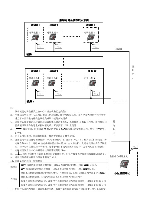
注:1、图中机房对讲主机及监控中心对讲主机由卖方提供;2、电梯机房至监控中心之间的布线(包括线材、线管及敷设工程)由客户按大楼结构尺寸负责,并且客户需协助电梯安装单位完成该功能的安装调试。
3、 敷线线缆为:PVC 护套屏蔽软电缆0.75mm 2的2芯电缆,型号为RVVP2×0.75。
4、此图适用于整个项目仅有6台或6台以下电梯的情况。
5、监控中心预留的通讯线需在到达对讲主机后,再多预留2米以上线缆;电梯机房预留的通讯线需在到达电梯控制柜后,再多预留2米以上线缆。
6、电梯机房到监控中心的最远布线距离不能超过2km 。
7、对于无机房电梯,电梯的控制柜一般放置在地面1楼井道内。
8、通讯线路单根内阻平均每百米不高于4Ω。
9、布线必需达到以下检测要求绝缘表500V 档分别测量接地线对黑线、白线及黑白两线间阻值,应在0.02M Ω以上。
万用表交流电压档测量黑、白线与接地线间的感应电压在48V 以内(电梯系统带电时测量)直流电压档测量黑、白线与接地线间及黑白两线间电压应为零短接各机房对讲主机通讯总线,在监控中心测量黑线、白线间阻值,应在120Ω之内10、如客户负责的布线部分需委托卖方完成,具体方案及价格需根据客户的实际要求,另行协商确定。
注4注4注4注4注4注4小区监控中心监控中心 对讲主机机房1控制柜1 机房对讲主机机房对讲主机控制柜y 通讯线弱电井1机房n弱电井n控制柜1 机房对讲主机控制柜y 机房对讲主机注4注4模拟对讲系统布线示意图2.3. 4. 5. 6. 7. 8. 9.10.11.12.2.3.4.5.6.7.8.9.10.11.12.13.14.15.16.17.18.19.20.21.22.23.24. 我知道你心里在想什么,师姐,你多半是骂我不知人事,不知这世道艰险,我心中所想所求,泰半都难有结果。
- 1、下载文档前请自行甄别文档内容的完整性,平台不提供额外的编辑、内容补充、找答案等附加服务。
- 2、"仅部分预览"的文档,不可在线预览部分如存在完整性等问题,可反馈申请退款(可完整预览的文档不适用该条件!)。
- 3、如文档侵犯您的权益,请联系客服反馈,我们会尽快为您处理(人工客服工作时间:9:00-18:30)。
对讲机原理图
对讲机是一种便携式通信设备,它利用无线电波进行通信。
对讲机的原理图包
括了发射机、接收机和天线等部件。
通过这些部件的协同工作,对讲机可以实现双向通信,使得用户可以在不同地点进行语音通信。
发射机是对讲机的核心部件之一,它负责将用户的语音信号转换成无线电波,
并通过天线发送出去。
发射机内部包含了话筒、音频放大器、调频调制器等部件,它们共同工作,将用户的语音信号转换成适合无线传输的信号,并通过天线发射出去。
接收机则是对讲机的另一个核心部件,它负责接收其他对讲机发送过来的无线
电波,并将其转换成可听的语音信号。
接收机内部包括了天线、射频放大器、解调器等部件,它们共同工作,将接收到的无线电波转换成可听的语音信号,并通过耳机或扬声器输出给用户。
除了发射机和接收机,对讲机的原理图还包括了天线等部件。
天线是对讲机的
信号收发器,它负责接收其他对讲机发送过来的无线电波,并发送自己的无线电波。
天线的设计和位置对对讲机的通信质量有着重要的影响,合理的天线设计可以提高对讲机的通信距离和质量。
总的来说,对讲机的原理图是一个复杂的系统,它包括了发射机、接收机、天
线等部件,它们共同工作,实现了对讲机的双向通信功能。
对讲机的原理图不仅是对讲机工作原理的具体体现,也是无线通信技术的一个重要应用。