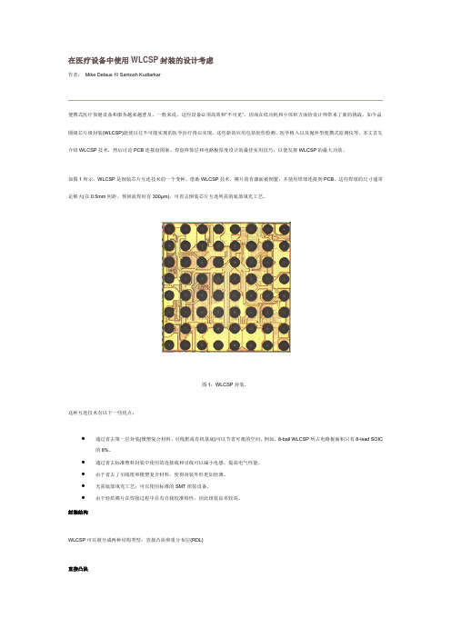
WLCSP器件焊点可靠性
什么是晶圆级芯片封装WLCSP

什么是晶圆级芯片封装WLCSP
随着移动电子产品趋向轻巧、多功能、低功耗发展,为了在更小的封装面积下容纳更多的引脚数,因而发展出晶圆级芯片封装WLCSP。
它具备更多的功能集成、在体积、成本和性能方面更具优势,可以应用在移动电话、蓝牙
产品、医疗设备、射频收发器、电源管理单元、音频放大器和GPS模块使用。
什幺是晶圆级芯片封装WLCSP呢?
大家可能比较熟悉BGA,CSP就是小型的BGA,外形和球间距比BGA 小,球间距小于0.8毫米的BGA称为CSP,或者封装面积和里面芯片的面积之比小于1.2。
至于WLCSP,就是晶圆级CSP,即是大型的倒装晶片,中间没有载体,
焊球直接植于硅基材上,一般焊球间距为0.4至0.8毫米间。
由于晶圆级芯片封装的密间距,其敏感度远远超过BGA。
那幺,在组装晶圆级芯片封装这种具有焊球直径小、焊球间距小、外形尺。
什么是晶圆级芯片封装WLCSP

什么是晶圆级芯片封装WLCSP
随着移动电子产品趋向轻巧、多功能、低功耗发展,为了在更小的封装面积下容纳更多的引脚数,因而发展出晶圆级芯片封装WLCSP。
它具备更多的功能集成、在体积、成本和性能方面更具优势,可以应用在移动电话、蓝牙产品、医疗设备、射频收发器、电源管理单元、音频放大器和GPS模块使用。
什么是晶圆级芯片封装WLCSP呢?
大家可能比较熟悉BGA,CSP就是小型的BGA,外形和球间距比BGA小,球间距小于0.8毫米的BGA称为CSP,或者封装面积和里面芯片的面积之比小于1.2。
至于WLCSP,就是晶圆级CSP,即是大型的倒装晶片,中间没有载体,焊球直接植于硅基材上,一般焊球间距为0.4至0.8毫米间。
由于晶圆级芯片封装的密间距,其敏感度远远超过BGA。
那么,在组装晶圆级芯片封装这种具有焊球直径小、焊球间距小、外形尺寸小的元器件特征时,厂家要注意什么呢?环球仪器提出了什么解决方案呢?
晶圆级芯片封装的装配流程
目前有两种工艺,一种是锡膏装配,但为了避免“桥连”或“少锡”缺陷,环球仪器建议采用助焊剂浸蘸的方法进行组装。
工艺流程:
拾取晶圆级芯片封装
浸蘸助焊剂
贴装晶圆级芯片封装
回流焊接
底部填充(如有需要)
在这里先集中讨论浸蘸助焊剂流程,环球仪器建议采用助焊剂薄膜浸蘸方式,即在元器件贴装前浸蘸一定厚度的助焊剂薄膜,使每个焊球上附着一定量的助焊剂。
采用助焊剂薄膜浸蘸的两大优点:。
晶圆级芯片级封装(WLCSP)在医疗设备设计的作用

晶圆级芯片级封装(WLCSP)在医疗设备设计的作用在医疗设备设计领域,一个重要趋势是提高这些设备的便携性,使其走近病人,进入诊所或病人家中。
这涉及到设计的方方面面,尤其是尺寸和功耗。
晶圆级芯片级封装(WLCSP)的运用对减小这些设备电子组件的尺寸起到了极大的助推作用。
此类新型应用包括介入性检测、医学植入体和一次性便携式监护仪。
但是为了最大限度地发挥出WLCSP封装在性能和可靠性方面的潜力,设计师必须在印刷电路板(PCB)焊盘图形、焊盘表面和电路板厚度的设计方面贯彻最佳实践做法。
图1. WLCSP封装晶圆级芯片级封装是倒装芯片互联技术的一个变体(图1)。
在WLCSP中,芯片活性面采用反转式设计,通过焊球连接至PCB。
一般地,这些焊球的尺寸足够大(0.5 mm间距,回流前为300 µm,0.4 mm间距,回流前为250 um),无需倒装互联技术所需要的底部填充。
该互联技术有多个优势。
首先,由于消除了第一级封装(塑封材料、引脚架构或有机基板),因而可以节省大幅空间。
例如,一个8引脚WLCSP所占电路板面积仅相当于一个8引脚SOIC的8%。
其次,由于消除了标准塑封中使用的线焊和引脚,因而可以减小电感,提高电气性能。
另外,由于消除了引脚架构和塑封材料,因而可以减轻重量,降低封装厚度。
无需底部填充,因为可以使用标准表贴(SMT)组装设备。
最后,低质芯片在焊锡固化期间具有自动对齐特性,有利于提高装配成品率。
封装结构WLCSP在结构上可分为两类:直接凸点和再分配层(RDL)。
直接凸点WLCSP包括一个可选的有机层(聚酰亚胺),充当芯片活性面的应力缓冲层。
聚酰亚胺覆盖着芯片上除焊盘周围开口之外的所有区域。
该开口上喷涂有或镀有一层凸点下金属(UBM)。
UBM由不同的金属层叠加而成,充当扩散层、阻挡层、浸润层和抗氧化层。
将焊球滴落(这是其称为落球的原因)在UBM上,并经回流形成焊接凸点(图2)。
图2. 直接凸点WLCSP图3. 再分配层(RDL) WLCSP运用RDL技术,可以把针对线焊设计的芯片(焊盘沿外围排列)转换成WLCSP。
晶圆级芯片封装技术(WL-CSP)电子教案

总结
• 在IC工艺线上完成的WL-CSP样品, 只是增加了重 布线和凸点制作两道工序, 并使用了两层BCB或PI 作为介质层和保护层, 整套工艺与IC芯片的制作技 术完全兼容, 所以它在成本、质量方面明显优于其 它CSP的制作工艺。
• WL-CSP工艺的倒装焊技术, 将芯片正面(有源区) 面向管座衬底作压焊焊接, 可充分发挥出超大规模 集成电路的高性能和新品质, 它不存在较大的电感、 电容和其它不希望有的特性。
晶圆级芯片封装技术(WL-CSP)
• 一、晶圆级芯片封装的定义 • 二、晶圆级芯片封装工艺 • 三、晶圆级芯片封装的可靠性
晶圆级芯片封装的定义
• 根据定义,晶圆级芯片封装就是芯片 尺寸的封装,其尺寸与芯片原尺寸相 同。基本概念是,在制造后,通常在 测试之前,马上取出晶片,再增加一 些步骤(金属和电介质层)产生一种结构, 就可将产品组装到电路板上。
• WL-CSP是在圆片前道工序完成后, 直接对圆片
利用半导体工艺进行后道工序, 再切割分离成单个 器件。因此, 采用WL-CSP能使产品直接从制造商 转入用户手中作全面测试。该项技术不但适应于 现有的标准表面贴装技术(SMT)设备, 而且也解决 了优质芯片问题。
• 圆片级器件和SMT进行大批量封装WL-CSP的封 装效率可达90%以上.
• 在所有的薄膜应用中最好采用聚合物,是由于 其非常低的介电常数和最小的损耗角正切值。
• 与干蚀刻材料相比,采用光敏聚合物, 要求更少的工艺处理步骤(可进行光刻) ,因此节省成本。
焊料凸点制作工艺
• 焊点制作可采用蒸发法、化学镀法、电镀 法、置球法和和焊膏模板印制法等。目前 仍以电镀法用得较多,该法2002年约占所有 焊料凸点制作法的70%(含金焊点制作), 其次是蒸发法(高铅),约占22.5%, 再者为 焊膏模板印制法, 约占5.5%。但因焊膏模板 印制法制作焊料凸点比较简便, 自动化程度 较高, 成本也较低, 故该法将会被较多地采 用。
电子器件封装工艺与实践考核试卷

D.光学显微镜
17.关于电子封装中的粘片工艺,以下哪项描述是正确的?( )
A.粘片工艺是在室温下进行的
B.粘片工艺使用的粘接剂为导电性粘接剂
C.粘片工艺主要用于陶瓷封装
D.粘片工艺不适用于高密度封装
18.以下哪种因素可能导致电子器件封装后的电性能下降?( )
A.焊接过程中的温度过高
B.封装材料的热膨胀系数过大
C.焊接过程中的温度控制
D.填充材料的选择
12.以下哪些情况可能导致电子封装的电气性能下降?( )
A.焊点缺陷
B.封装材料老化
C.基板污染
D.封装内部湿气
13.以下哪些封装形式具有较好的抗干扰性能?( )
A. BGA封装
B. QFN封装
C. LGA封装
D. DIP封装
14.电子封装中,以下哪些方法可以提高散热效率?( )
( )
2.描述电子封装中焊点缺陷的常见类型,并分析可能导致这些缺陷的原因。
( )
3.论述在电子封装过程中,如何通过控制工艺参数来提高封装的可靠性和热性能。
( )
4.请解释为什么无铅焊料逐渐取代了传统的铅锡焊料,并讨论无铅焊料在实际应用中可能遇到的问题和挑战。
( )
标准答案
一、单项选择题
1. A
2. B
A.打线焊接是在室温下进行的
B.打线焊接使用的是高熔点焊料
C.打线焊接是通过机械力来实现焊点连接
D.打线焊接主要应用于表面贴装技术
8.下列哪种封装形式通常具有较好的电磁屏蔽效果?( )
A. QFN封装
B. SOP封装
C. DIP封装
D. BGA封装
9.在电子封装过程中,以下哪种情况可能导致芯片损坏?( )
在医疗设备中使用WLCSP封装的设计考虑
在医疗设备中使用WLCSP封装的设计考虑作者:Mike Delaus和Santosh Kudtarkar便携式医疗保健设备和服务越来越普及。
一般来说,这些设备必须高效和“不可见”,因而在低功耗和小体积方面给设计师带来了新的挑战。
如今晶圆级芯片级封装(WLCSP)能使以往不可能实现的医学治疗得以实现。
这些新的应用包括创伤检测、医学植入以及抛弃型便携式监测仪等。
本文首先介绍WLCSP技术,然后讨论PCB连接盘图案、焊盘终饰层和电路板厚度设计的最佳实用技巧,以便发挥WLCSP的最大功效。
如图1所示,WLCSP是倒装芯片互连技术的一个变种。
借助WLCSP技术,裸片的有源面被倒置,并使用焊球连接到PCB。
这些焊球的尺寸通常足够大(在0.5mm间距、预回流焊时有300μm),可省去倒装芯片互连所需的底部填充工艺。
图1:WLCSP封装。
这种互连技术有以下一些优点:∙通过省去第一层封装(模塑复合材料、引线框或有机基底)可以节省可观的空间。
例如,8-ball WLCSP所占电路板面积只有8-lead SOIC 的8%。
∙通过省去标准塑料封装中使用的连接线和引线可以减小电感、提高电气性能。
∙由于省去了引线框和模塑复合材料,使得封装外形更加轻薄。
∙无需底部填充工艺;可以使用标准的SMT组装设备。
∙由于轻质裸片在焊接过程中具有自我校准特性,因此组装良率较高。
封装结构WLCSP可以被分成两种结构类型:直接凸块和重分布层(RDL)直接凸块直接凸块WLCSP包含一个可选的有机层(聚酰亚胺),这个层用作有源裸片表面上的应力缓冲器。
聚酰亚胺覆盖了除连接焊盘四周开窗区域之外的整个裸片面积。
在这个开窗区域之上溅射或电镀凸块下金属层(UBM)。
UBM是不同金属层的堆叠,包括扩散层、势垒层、润湿层和抗氧化层。
焊球落在UBM之上(因此叫落球),然后通过回流焊形成焊料凸块。
直接凸块WLCSP的结构如图2所示。
图2:直接凸块WLCSP。
重分布层(RDL)图3是一种重分布层(RDL)WLCSP。
WLCSP器件Sn3.9Ag0.6Cu焊点疲劳寿命预测
行词汇教学时, 一定要让学生在 情境中 学习词汇, 这样不 ! 仅能使学生准确地理解, 地记忆, 牢固 还能使学生掌握语 !
言使用的场合。 教师首先要设置词汇使用的情境, 然后可 , . 、, ! 以根据情境 对学生提 问 . 展现词 汇使用 的情境 , 最后教 师
点不再像初中、 高中那样讲解和大量练习, 而是培养学生 学习语法 的能力 , 指导学 生学会适 当归纳和总结 。 教师教
箭双雕 ” 。 输入 与输 出是 同时进行 的 , 并不是先输入 , 达到一定
作者 简介 : 立芬( 9 9 ) 女 , 顾 17 一 , 辽宁锦 州人 , 士 , 硕 主要从 事外 国语 言学与应 用语 言学研 究。
教师可 以尝试着把课 堂交 给学生 ,积极鼓励学 生走 上讲 台去讲 课 , 老师就从 “ 这样 知识 的传授者 ” 为“ 转 智慧 的启迪者 ” 以这种“ 生互换角 色” , 师 的教学方式来 转变学 生 的学 习方 式 , 学生 由传统 的“ 使 你讲我 听 ” 的被 动学 习
方 式转变为 积极主动学 习 ,也为提升学生 的交 际能力提 供 足够 的空间 () 3 开展丰富 多彩 的活动
输入前 提 出要求 。 以让 学生带着 问题 去听和读 , 可 也 可 以让其 先听后读 , 然后教师 提问题或提要求 。 输入 量要充分 。 如果课上 时间不够 , 课下要布置 阅读 和听力作 业 ; 而且要经常检查 , 至要 记下平时成绩 。 甚 事实证 明 , 与其花大量课 上时间讲语法 知识 , 不如让
辽辽
丁 丁
高职高专公共英语教学方法再探讨
顾 Байду номын сангаас芬
( 阜新高等专科 学校 外语 系, 宁 阜新 13 0 ) 辽 2 0 0
SnAgCu-nano Al钎料Anand本构关系及焊点可靠性

SnAgCu-nano Al钎料Anand本构关系及焊点可靠性张亮;韩继光;郭永环;何成文【摘要】In this paper, the constitutive relation of SnAgCu-nano Al is investigated and the constitutive model is used in the finite element simulation to analyze the stress-strain response in FCBGA devices. The results show that the nine parameters of the Anand model can be fitted based on nonlinear data fitting method with different temperature and strain rate. Combining Anand model, the stress-strain response of solder joints is calculated by using the finite element method, and it is found that the distribution of stress-strain of solder joints in FCBGA device can be affected by the solder joints array, i.e., the maximum stress-strain concentrates in the concern solder joints. The results also demonstratethat the stress-strain of SnAgCu-nano Al solder joints is lower than that of SnAgCu solder joints, which implies that the addition of nano Al particles can enhance the reliability of SnAgCu solder joints.%研究了含纳米0.1 wt.%Al颗粒SnAgCu无铅钎料Anand本构关系,将本构关系应用于有限元模拟,分析FCBGA器件SnAgCu-nano Al焊点的应力-应变响应。
- 1、下载文档前请自行甄别文档内容的完整性,平台不提供额外的编辑、内容补充、找答案等附加服务。
- 2、"仅部分预览"的文档,不可在线预览部分如存在完整性等问题,可反馈申请退款(可完整预览的文档不适用该条件!)。
- 3、如文档侵犯您的权益,请联系客服反馈,我们会尽快为您处理(人工客服工作时间:9:00-18:30)。
Rate-dependent properties of Sn–Ag–Cu based lead-free solder joints for WLCSPY.A.Su a ,L.B.Tan a ,T.Y.Tee b ,V.B.C.Tan a,*a National University of Singapore,Department of Mechanical Engineering,9Engineering Drive 1,Singapore 117576,Singapore bAmkor Technology,Inc.,2Science Park Drive,Singapore 118222,Singaporea r t i c l e i n f o Article history:Received 22July 2009Received in revised form 18January 2010Available online 24February 2010a b s t r a c tThe increasing demand for portable electronics has led to the shrinking in size of electronic components and solder joint dimensions.The industry also made a transition towards the adoption of lead-free solder alloys,commonly based around the Sn–Ag–Cu alloys.As knowledge of the processes and operational reli-ability of these lead-free solder joints (used especially in advanced packages)is limited,it has become a major concern to characterise the mechanical performance of these interconnects amid the greater push for greener electronics by the European Union.In this study,bulk solder tensile tests were performed to characterise the mechanical properties of SAC 105(Sn–1%wt Ag–0.5%wt Cu)and SAC 405(Sn–4%wt Ag–0.5%wt Cu)at strain rates ranging from 0.0088s À1to 57.0s À1.Solder joint array shear and tensile tests were also conducted on wafer-level chip scale package (WLCSP)specimens of different solder alloy materials under two test rates of 0.5mm/s (2.27s À1)and 5mm/s (22.73s À1).These WLCSP packages have an array of 12Â12solder bumps (300l m in diameter);and double redistribution layers with a Ti/Cu/Ni/Au under-bump metallurgy (UBM)as their silicon-based interface structure.The bulk solder tensile tests show that Sn–Ag–Cu alloys exhibit higher mechanical strength (yield stress and ultimate tensile strength)with increasing strain rate.A rate-dependent model of yield stress and ultimate tensile strength (UTS)was developed based on the test results.Good mechanical perfor-mance of package pull-tests at high strain rates is often correlated to a higher percentage of bulk solder failures than interface failures in solder joints.The solder joint array tests show that for higher test rates and Ag content,there are less bulk solder failures and more interface failures.Correspondingly,the aver-age solder joint strength,peak load and ductility also decrease under higher test rate and Ag content.The solder joint results relate closely to the higher rate sensitivity of SAC 405in gaining material strength which might prove detrimental to solder joint interfaces that are less rate sensitive.In addition,speci-mens under shear yielded more bulk solder failures,higher average solder joint strength and ductility than specimens under tension.Ó2010Elsevier Ltd.All rights reserved.1.IntroductionElectronic components are shrinking in size to meet demands for lightweight and feature filled portable electronic products.This leads to decreasing solder joint dimensions,where mechanical reli-ability has become an issue [1],especially under high strain rate conditions during testing,transport and handling,impact loading under automotive [2]and consumer portable applications.Tin lead alloy (SnPb)was commonly used as a solder material in microelectronic packaging,but it is also hazardous to the environ-ment and health.Therefore,the industry made a transition to lead-free solders,with the implementation a ban on lead (Pb)from elec-tronic products by the EU RoHS (restriction of the use of certain hazardous substances in electrical and electronic equipment)inJuly 2006.The transition to lead-free solders is led by the widely adopted Sn–Ag–Cu (SAC)eutectic [3].However,some studies have shown that standard SAC alloys such as SAC 405(Sn–4%wt Ag–0.5%wt Cu)have poorer mechanical performance than eutectic SnPb under high strain rate conditions [4].Moreover,with the increasing popularity of portable devices,the performance of Sn–Ag–Cu solder joints under high strain rate and large rate ranges typical of drop impact situations is a major concern.In this study,dogbone-shaped bulk material tensile tests were conducted to investigate the effect of strain rate and silver content on the material properties of Sn–Ag–Cu solders.Solder joint array shear and tensile experiments were conducted on WLCSP speci-mens of different alloy materials under different strain rates and loading orientations to investigate the effects of strain rate,silver content in Sn–Ag–Cu solder joints,and loading orientation on microelectronic packages.Failure analyses were also performed on the fractured dogbone-shaped bulk material test specimens and WLCSP solder joints.0026-2714/$-see front matter Ó2010Elsevier Ltd.All rights reserved.doi:10.1016/j.microrel.2010.01.043*Corresponding author.E-mail address:mpetanbc@.sg (V.B.C.Tan).Microelectronics Reliability 50(2010)564–576Contents lists available at ScienceDirectMicroelectronics Reliabilityjournal homepage:w w w.e l s e v i e r.c o m /l oc a t e /m i c r o r el2.Experimental details and methodology2.1.Test methodology for dogbone-shaped bulk solder tensile test Dogbone-shaped bulk solder specimens were used to perform tensile tests to characterise the mechanical properties of SAC 105and SAC 405.The bulk solder specimens had a gauge length of 19mm and diameter of 3mm as shown in Fig.1.The specimens were fabricated by machining from solder ingots and annealed at 70°C for 24h to reduce residual stresses.The bulk solder tensile tests were conducted on a universal tes-ter.Three to four samples were tested at various test rates from 10mm/min (0.0088s À1)to 65,000mm/min (57.0s À1).2.2.Test methodology for solder joint array shear and tensile test Package pull and shear tests were conducted on wafer-level chip scale packages (WLCSP)with SAC 105or SAC 405alloy solder joints at 0.5mm/s and 5mm/s.Solder joint strength and ductility data are collected and failure analysis (FA)of the WLCSP joints performed via optical microscopy and SEM.The FA findings are then statisti-cally tabulated and jointly analysed and correlated with test results.The WLCSP specimens were sawed out from board assemblies which were as-reflowed,unaged and non-solder mask defined,as shown in Fig.2.Each WLCSP specimen had an array of 12Â12sol-der joints sandwiched between a die substrate and a printed circuit board.These WLCSP packages have solder bumps that are 300l m in diameter and double redistribution layers with a Ti/Cu/Ni/Au under-bump metallurgy (UBM)as their silicon-based interface structure.The test samples were bonded onto fixtures using a cyanoacry-late base adhesive and tested on an Instron Microtester.Specimens of two solder alloy materials (SAC 105and SAC 405)were tested at room conditions.Two to three samples were tested for each test parameter.The tests were carried out at test rates of 0.5mm/s (2.27s À1)and 5.0mm/s (22.73s À1)and two loading orientations of shear and tension,as shown in Fig.3.3.Results and discussion3.1.Dogbone-shaped bulk solder tensile test resultsThe dogbone-shaped bulk solder specimens were tested un-der four test rates,with four samples per test rate.Nominal stress–strain data were derived from the load–displacementraw data and plotted as shown in Fig.4a ,where the mechanical properties such as yield stress and ultimate tensile strength (UTS)were obtained.Yield stress was obtained at the point of 0.5%offset.True stress–strain curves were also plotted for comparison.3.1.1.Effect of strain rate on bulk solder material propertiesFig.4b shows the true stress–strain curves of SAC 405,where the most representative sample curves of each of the four test rates were extracted and combined.It is observed that strain rate affects the bulk solder material properties,with increasing strength at higher rate of loading.Both Pang [5]and Che [6]had performed similar dogbone-shaped bulk solder tensile tests and also showed that material properties such as the yield stress and UTS of Sn–Ag–Cu solder alloys increase at higher strain rates.3.1.1.1.Rate-dependent model development.Mechanical properties such as yield stress and UTS have linear logarithmic/power relationship with respect to strain rate.As such,a rate-dependent model can be developed to express this relationship quantitatively.NomenclatureSn–Ag–Cu tin–silver–copper (Sn–Ag–Cu)alloy WLCSP wafer-level chip scale package r y yield stress,MPa r UTS ultimate tensile stress,MPa _e strain rate,s À1Std.dev.standard deviationDTBTSR ductile to brittle transition strain rateSEM scanning electron microscope UBM under-bump metallization IMC inter-metallic compound Cu RDL copper redistribution layerA T total failure cross sectional area,m 2r aveaverage solder joint array strength,MPaF maxpeak load from solder joint array shear and tensile tests,NFig.1.Dimensions of dogbone bulk solderspecimen.Fig.2.Printed circuit board assembly and sawed WLCSP testspecimen.Fig.3.Schematic of solder joint array shear and tensile tests.Y.A.Su et al./Microelectronics Reliability 50(2010)564–576565This is expressed in logarithmic scale as shown in Figs.5a and5b. Different solder alloy materials exhibit similar linear trend,with yield stress and UTS increasing at higher strain rate.The yield stress and UTS relationships with strain rate are obtained through curvefitting of the plots in Figs.5a and5b respectively to give:r yð_eÞSn—Ag—0:5Cu¼b1logð_eÞþb2ð1ÞrUTSð_eÞSn—Ag—0:5Cu¼c1logð_eÞþc2ð2ÞFor ease of comparison with existing literature,the rate depen-dence in yield stress and UTS can be further expressed in the fol-lowing power relationships:r yð_eÞSn—Ag—0:5Cu¼b3ð_eÞb4ð3ÞrUTSð_eÞSn—Ag—0:5Cu¼c3ð_eÞc4ð4ÞThe coefficients b1,b2,c1,c2,b3,b4,c3and c4are listed in Table1.The material parameters of SAC105and Amkor’s internal data for SAC305are compared with the results obtained by Che[6], which are presented in Table2.The development of such a rate-dependent model allows for better understanding of the relationships between mechanical properties and strain rate of applied loading.This enables the pre-diction of the mechanical properties at the strain rate of interest.It also enables the comparison of experimental results across similar literature.3.1.1.2.Strain rate sensitivity.Referring to Figs.5a and5b,the high-er gradient of the linear curves translate to larger increase in strength with a given increase in strain rate,which can also be ex-pressed as higher strain rate sensitivity of material strength.The coefficients b1and c1correspond to the gradient of the linear curves,which also directly relate to the strain rate sensitivity of yield stress and UTS respectively.Strain rate sensitivity can be use-ful in the study of the ductile to brittle transition strain rate (DTBTSR)in solder joints,which is affected by the sensitivity of bulk solder strength to strain rate,as depicted in Fig.12a.3.1.2.Effect of Ag content on mechanical properties of bulk solderFigs.5a,5b,6a and6b show the effect of silver(Ag)content on the yield stress and UTS of Sn–Ag–Cu solder alloy.Silver(Ag)con-tent of1%corresponds to SAC105and4%corresponds to SAC405. The yield stress and UTS of4%Ag content(SAC405)are consis-tently higher than1%Ag content(SAC105).Therefore,yield stress and UTS increase with higher Ag content in Sn–Ag–Cu alloys.Che[6]had also obtained results that show higher yield stress, UTS and lower elongation(equivalent to ductility)in Sn–Ag–Cu al-loys with higher Ag content.Sn–Ag–Cu alloys have three phases of primary Sn,Ag3Sn and Cu6Sn5[4].Suh[4]had presented the mechanical properties of the three phases of Sn–Ag–Cu micro-structure and primary Sn has the lowest elastic modulus and strength of the three phases.Sn–Ag–Cu alloys are strengthened by the internal stress accumulated due to the difference in elastic modulus and volume fraction between Ag3Sn and Sn matrix[7]. Higher Ag content will increase the amount of Ag3Sn phase[2] and also lower the amount of primary Sn phase in Sn–Ag–Cu solder alloys[4].SAC105,with lower Ag content,is expected to have less Ag3Sn and more primary Sn phase.This contributes to the lower566Y.A.Su et al./Microelectronics Reliability50(2010)564–576strength of SAC 105compared to Sn–Ag–Cu alloys with higher Ag content [4].3.1.3.Failure analysis of fractured dogbone-shaped bulk solder test specimensPhotographs of the fractured dogbone-shaped bulk solder test specimens were taken under an optical microscope.The sideviews/overviews and closeup views of the specimens are presented in Fig.7.It is generally observed that 45°shearing is the primary mode of failure at low test/strain rates while necking is mostly ob-served at higher test/strain rates.At low strain rates,the solder al-loy is able to undergo slip deformation across the whole cross section of the dogbone shaped specimen,resulting in 45°shearing.As Sn–Ag–Cu alloy materials have high homologous temperature,there is not much strain hardening under low strain rate loading.At higher strain rates,the material is not able to respond to the ap-plied loading by slip deformation and experiences greater strain hardening,therefore necking occurs.From Fig.7,it can be observed that the diameter of fracture generally decreases at higher test/strain rate due to necking.3.2.Solder joint array shear and tensile test results3.2.1.Failure analysis of WLCSP jointsOptical microscopy and scanning electron microscopy (SEM)were used to examine the fractured solder joints,which are around 0.3mm in diameter each.Three modes of failure were identified and categorised,namely:(1)bulk solder failure,(2)UBM IMC fail-ure and (3)pad matrix failure.Although there are other less pre-vailing failure modes observed (such as Cu RDL and Pad IMC),the three failure modes are chosen to be analysed due to their high frequency of occurrence (adding up to >90%of the failure modes of all the solder joints).They are also the most common failures iden-tified by researchers [8,9].Images of the respective failure modes at both the die/substrate side and board side were taken under the optical microscope and scanning electron microscope (SEM),as shown in Fig.8a–c .The photographs and SEM images are accompanied by cross sectional schematics to show the location of each failure mode.3.2.1.1.Bulk solder failure.Bulk solder failure occurs by fracturing through the solder sphere as shown in Fig.8a.These failures are usually detected near the die side interface and can be easily iden-tified by the silvery solder residue on the die substrate.From the board side,it can be recognised by the uneven fracture surface on the solder bump that is still attached to the board.3.2.1.2.UBM IMC (under-bump metallization intermetallic compound)failure.Brittle interface failure occurs at the interfacial regions be-tween the bulk solder and the die substrate.The failure crack usu-ally occurs in the intermetallic compounds (IMC)or at the interfaces with the substrate.These intermetallic compounds are usually more brittle than the bulk solder [1].UBM IMC failure refers to fracture at the intermetallic com-pound (IMC)interface layer between the UBM layer and the bulk solder.It can be identified by a smooth grey surface on the die sub-strate.From the board side,it can also be identified by its charac-teristic ring step and smooth surface at the top of the solder bump,shown in Fig.8b.3.2.1.3.Pad matrix failure.Pad matrix failure is failure in the pad re-sin at the printed circuit board.It occurs at the matrix of the com-posite that makes up the board.It is identified by the distinct redTable 1Material parameters of rate dependent yield stress and UTS of different solder alloys.Logarithmic Power Yield stress UTS Yield stress UTS b 1b 2c 1c 2b 3b 4c 3c 4SAC 105 2.92241.373 4.17454.71740.3780.077553.0930.081SAC 4052.97349.8645.29572.21348.7410.059669.6330.0779Table 2Comparison of material parameters of rate dependent yield stress and UTS of different solder alloys between Amkor’s data and Che’s data based on Eqs.(3)and (4).Yield stress UTS AmkorChe Std.dev.Amkor Che Std.dev.b 3b 4SAC 10540.3832.15 5.8190.07750.05130.01853SAC 30552.74643.32 6.6650.07150.04450.01909c 3c 4SAC10553.09353.990.6340.0810.09180.00764SAC30570.25860.187.1260.07770.06080.01195Y.A.Su et al./Microelectronics Reliability 50(2010)564–576567copper pad on the solder bump that is attached to the die.It can also be identified by ‘cratering’[3]in the board side,as shown in Fig.8c.Solder joints that were fractured during tests were examined to determine their modes of failure.Both Zhao [9]and Darveaux [8]had identified three major modes of solder joint failures forballFig.7.Photographs of fractured dogbone-shaped bulk solder tensile testspecimens.Fig.8.Schematic diagram of:(a)bulk solder failure,(b)UBM IMC failure and (c)pad matrix failure on die substrate,board,and solder joint cross section.568Y.A.Su et al./Microelectronics Reliability 50(2010)564–576grid array packages (BGAs),namely ductile bulk solder failure,brit-tle interface fracture at the intermetallic compound (IMC)layer and pad failure,shown in Fig.9.Bulk solder failure is commonly regarded as a desirable mode of failure.A ductile bulk solder will deform when loading is applied,and this will minimise stresses in the interfacial regions due to bet-ter package/PCB curvature compliance.As failure in interfacial re-gions can occur under relatively small strain displacements and under rapid crack propagation rate,it will be preferable to reduce their occurrence to avoid catastrophic failures [8].Wong et al.noted that bulk solder failures correspond to high drop test life of ball grid array packages (BGAs),which is more desirable than IMC failures that correspond to low drop test life [10].Therefore,the observation of bulk solder failure is often related to better reli-ability of solder joints under high strain rate conditions.3.2.2.Derivation of average solder joint array strengthThe package pull/shear tests yielded load–displacement raw data,where the peak load was recorded.Darveaux had calculated the average stress in the solder joint array by dividing load over the sum of joint pad area [2].In this study,the WLCSP solder joint has varying cross sectional dimensions at the different regions of failure as shown in Fig.10.The number of solder joints that failed under each mode (n i )were counted based on photographs taken using an optical microscope,shown in Figs.11a and 11b .The fail-ure mode count (n i )was subsequently multiplied by the cross sec-tional area of that failure region in a single solder bump (a i ),to obtain the total affected cross sectional area for that particular mode of failure (A i ).The total failure cross sectional area (A T )can be obtained by summing up the failure cross sectional area of each failure mode (A i ).Total failure cross sectional area,A T ¼XiA i ¼Xia i n i ð5Þwhere i =1corresponds to failure mode 1(e.g.bulk solder failure),i =2corresponds to failure mode 2(e.g.UBM IMC failure),etc.The average solder joint array strength (r ave )is calculated by dividing peak load (F max )over the total failure cross sectional area,A T .Average solder joint array strength,r ave ¼F max Tð6ÞThe peak loads obtained from the tests and the resulting peak stresses derived are given in Table 3.As shown in the preceding paragraphs,there is a distinction be-tween bulk solder strength and solder joint strength.Bulk solder strength refers to the strength of the solder alloy in resisting fail-ure,whereas solder joint strength refers to the strength of the en-tire solder joint that consists of a multitude of different materials making up the joint,such as that of the bulk solder,PCB Cu pad,UBM,RDL Polyimide layer dielectric,and silicon die.Further,fail-ure of the solder joint may not lie within a particular material,but at the interfaces,e.g.UBM/RDL,solder/IMC,etc.Hence,a strong solder alloy may not necessarily create a strong and reliable solder joint.In general,solder joint reliability depends on its components’mechanical properties and interaction,and the proper selection of solder alloys and their properties on a particular joint structure and make-up would improve solder jointlife.Fig.10.Typical cross sectional diameters of WLCSP solderjoint.Fig.11a.Fractured solder joint array specimen after shear test (dieside).Fig.11b.Fractured solder joint array specimen after shear test (padside).Fig.9.Schematic of bulk solder failure and interface failures.Y.A.Su et al./Microelectronics Reliability 50(2010)564–5765693.2.3.Effect of strain rate3.2.3.1.Ductile to brittle transition.Sn–Ag–Cu solder alloys gener-ally attain higher strength at higher strain rates [6,5].This is repre-sented in Fig.12a as an upward sloping line.At low strain rates,bulk solders have low strength,resulting in predominant failure in the bulk solders,depicted as ‘100%bulk solder failure’in Fig.12b .At higher strain rates,the bulk solders are stronger and more resistant to mechanical loading.The gain in strength also re-sulted in less deformation and compliance for the solder,and the applied loading stress will increasingly accumulate at the solder joint interfaces [8]due to their proximity to geometric discontinu-ities,resulting in more interfacial failures than bulk solder failures.As the test rates increases,there will eventually be no more bulk solder failures,being replaced entirely by failures occurring at the interface regions,depicted by ‘100%interface failure’in Fig.12b .As such,there is a transition from predominant ductile bulk solder failures to brittle interface failures with increasing strain rate,as shown in Fig.12b .Darveaux had investigated the ductile to brittle transition strain rate (DTBTSR)by performing solder joint array tensile tests [2].The ductile to brittle transition strain rate (DTBTSR)was defined as the strain rate at which,50%of the joints fail at the pad interface’[2].In this study,‘ductile to brittle transition strain rate’will simply be the strain rate where 50%of the joints fail at the bulk solder,‘inter-facial failure’will collectively refer to all the other non bulk solder modes of failure.It can be seen that the value of DTBTSR is a good gauge of what application strain rate the particular structure of solder joints can withstand before they start to fail abruptly at the joint interfaces.Knowledge of the DTBTSR values will allow researchers to design their packages to avoid excessive strain rate ranges that the joint would not be able to handle.As it would be desirable to register a relatively high peak load and observe bulk solder failures in solder joints under high strain rate loading,from Fig.12b ,the preferred outcome then would be to design solder joints to have a higher ductile to brittle transition strain rate (DTBTSR)[8]for improved reliability under high strain rate conditions.3.2.3.2.Effect of strain rate on solder joint array strength.Figs.13a and 13b show the average solder joint array strength of the tested specimens at two different test rates (0.5mm/s and 5.0mm/s)un-Fig.12a.Diagram of ductile to brittle transition in the relationship between solder joint strength and strain rate (adapted from [2]).Fig.12b.Diagram of ductile to brittle transition in the relationship between %bulk solder failures and strain rate (adapted from [2]).Table 3Solder joint array shear and tensile test results and derivation of average solder joint array strength.Solder alloyLoading orientationTest rate (mm/s)Average solder joint array strength,r ave (MPa)Failure mode count,n i Bulk solderUBM IMC Cu RDL Pad matrix SAC 405Shear 539.4401083330.543.663510107Tension58.960001440.556.77060139SAC 105Shear 536.890644770.554.79750070Tension517.110511390.542.36331111‘Pad IMC’mode of failure is not observed for SAC 105and SAC 405.570Y.A.Su et al./Microelectronics Reliability 50(2010)564–576der shear and tension.It is observed that the average solder joint array strength decreases at higher test/strain rates,regardless of solder alloy material and test orientation.Newman had observed higher strength at higher shear rates in solder ball impact shear tests [11],and Darveaux also obtained similar trend in solder joint array tensile tests [8].However,Darveaux also noted that solder joint strength declined at even higher strain rates when ‘interface failures start to occur’[8].From the experiments conducted in this study,interface failures had already started to occur in all the test specimens under the test rates of 0.5mm/s and 5mm/s.The test/strain rates employed in this study (0.5mm/s and 5mm/s)may al-ready be high enough to lead to the decline in average solder joint array strength.Referring to Fig.12a of the ductile to brittle transition strain rate model,it can be seen that beyond the DTBTSR,there is a fall in interface strength of solder joints.Coupled with the increase in the amount of interface failures (see Fig.12b or Fig.17),this will lead to a decline in combined solder joint array strength at higher strain rate.The solder joint array test results in Figs.13a and 13b have also shown that average solder joint strength declined with higher test/strain rate.3.2.3.3.Effect of strain rate on failure mode (under shear).(1)Bulk solder failure.Fig.14a shows the percentage of bulk solder failures observed for the two different solder alloy solder joints tested under shear.At the higher test rate of 5mm/s,there is almost no more failure at the bulk solder,implying that all failures occur at the interfa-cial regions.As bulk solder becomes more load resistant and experience less deformation,it is less susceptible to mechanical failure at higher strain rates.In the transition from ductile to brittle failure,there is a decrease in bulk solder failures to even-tually no more bulk solder failure at higher strain rates [2],as shown in Fig.12b .This is also depicted in Fig.14b ,in which the experimental result of SAC 105from Fig.14a is superimposed onto Fig.12b of the ductile to brittle transition strain rate model.Fig.14b shows that the experimental results of SAC 105follow a similar trend as the ductile to brittle transition strain rate model.(2)UBM IMC failure.Fig.14c shows the percentage of UBM IMC failures for the dif-ferent alloy solder joints under shear.Such failure modes are prominent at higher shear application rates due to the transition from ductile (cohesive)to brittle (interface)failures at increasingly higher strain rates.Fig.14b.Experimental result of SAC 105(under shear)superimposed onto the ductile to brittle transition strain ratemodel.Y.A.Su et al./Microelectronics Reliability 50(2010)564–576571(3)Pad matrix failure.In Fig.14d,pad matrix failure is observed to be increasingly dominant for SAC105as the test rates increases for shear.In contrary,SAC405has a reduction of pad matrix failures at the higher test rate of5mm/s,as a result of a corresponding predom-inance of UBM IMC failures(see Fig.14c),which is also an interfa-cial mode of failure.From thefigures for SAC405,the predominant failure mode changes from pad matrix failure at0.5mm/s to UBM IMC failure at5mm/s.(see Fig.14c).The observed failure modes transition may be a result of the UBM IMC layer being weaker than pad ma-trix layer at the higher test rate of5mm/s for SAC405.It is sur-mised that the higher rate sensitivity of SAC’s405mechanical strength may have contributed to the mode transition that is not yet observable for solder joints of the other two alloys.Essentially,interfacial failures such as UBM IMC and pad matrix failures become more dominant at higher strain rates,due to the strengthening of the bulk solder.Thefinal failure location depends on the components mechanical characteristics and is a competition among the different interfacial regions for failure as they share the applied load.Figs.14e and14f shows the percentage of interface failures (UBM IMC and pad matrix failures)of SAC405and SAC105respec-tively at the two test rates under shearing.There is a higher per-centage of interface failures at the higher test rate.Non bulk solder modes of failures such as UBM IMC and pad matrix failures are interfacial failures that become more dominant at higher strain rate,due to the strengthening of the bulk solder.This is similar to Figs.12b and14b,depicting the transition from ductile to interface failures in solder joints at higher strain rates.3.2.3.4.Effect of strain rate on failure mode(under tension).(1)Bulk solder failure.No bulk solder failure is observed for the two test rates.It is likely that the designated test rates of0.5mm/s and5mm/s have already surpassed the ductile to brittle transition strain rate (DTBTSR)for the three different alloyed joints and hence experi-ence100%interface failures shown in Fig.12b.In Fig.15a,the experimental result of SAC105is superimposed onto Fig.12b of the ductile to brittle transition strain rate model.Fig.15a also shows that the experimental results of SAC105correlates with the ductile to brittle transition strain rate model.Fig.15a.Experimental result of SAC105(under tension)superimposed into the ductile to brittle transition strain rate model.572Y.A.Su et al./Microelectronics Reliability50(2010)564–576。