Direct current voltage induced by microwave signal in a ferromagnetic wire
GS4157 4157B 低电压、2.8Ω双极性SPDT分析开关说明书

GS 4157/4157BLow-Voltage, 2.8Ω SPDT Analog SwitchGeneral DescriptionThe GS 4157/4157B is a high-bandwidth, fast single-pole double-throw (SPDT) CMOS switch. It can be used as an analog switch or as a low-delay bus switch. Specified over a wide operating power supply voltage range, 1.65V to 5.5V, the GS 4157/4157B has a maximum ON resistance of 5.1-ohms at 1.65V, 3.9-ohms at 2.3V & 2.85-ohms at 4.5V. Break-before-make switching prevents both switches being enabled simultaneously. This eliminates signal disruption during switching.The control input, S, tolerates input drive signals up to 5.5V, independent of supply voltage. GS 4157/4157B is an improved direct replacement for the FSA4157/NC7SB4157ApplicationsCell Phones PDAsPortable InstrumentationBattery Powered Communications Computer PeripheralsConnection Diagram(Top View)SC70-6 65S VCC 4AGND 3B0B121TDFN-6Features♦CMOS Technology for Bus and Analog Applications♦LowONResistance:***********♦Wide VCC Range: 1.65V to 5.5V ♦Rail-to-Rail Signal Range♦Control Input Overvoltage Tolerance: 5.5V min.♦High Off Isolation: 57dB at 10MHz♦54dB (10MHz) Crosstalk Rejection Reduces Signal Distortion♦Break-Before-Make Switching ♦High Bandwidth: 300 MHz♦Extended Industrial Temperature Range: –40°C to 85°C♦Improved Direct Replacement for NC7SB4157♦Packaging (Pb-free & Green available):Pin DescriptionLogic Function TableLogic Input (S)Function 0 B0 Connected to A 1B1 Connected to ANameDescription S Logic ControlVcc Positive Power Supply ACommon Output/Data Port B0 Data Port (Normally Closed) GND Ground B1Data PortABSOLUTE MAXIMUM RATINGS(1) RECOMMENDED OPERATING CONDITIONS(3)Supply Voltage V CC.........................................–0.5V to +7V DC Switch Voltage (V S)(2).…….......…..–0.5V to V CC +0.5V DC Input Voltage (V IN)(2).…..…….....….......–0.5V to +7.0V DC V CC or Ground Current (I CC/I GND)..................±100mA DC Output Current (V OUT) .......................................128mA Storage Temperature Range (T STG) ....... –65°C to +150°C Junction Temperature under Bias (T J) .......…............ 150°C Junction Lead Temperature (T L)(Soldering, 10 seconds) .................................... 260°C Power Dissipation (P D) @ +85°C .............................180mW Supply Voltage Operating (V CC)………………1.65V to 5.5V Control Input Voltage (V IN)………………………..0V to V CC Switch Input Voltage (V IN)…………………………0V to V CC Output Voltage (V OUT)…………………………….0V to V CC Operating Temperature (T A)………………...–40°C to +85°C Thermal Resistance (θJA)…………………………..350°C/WNote 1:A bsolute Maximum Ratings” may cause permanent damage to the device. This is a stress only rating and operation of the device at these or any other conditions beyond those indicated in the operational sections of this specification is not implied.Note 2:The input and output negative voltage ratings may be exceeded if the input and output diode current ratings are observed.Note 3:Control input must be held HIGH or LOW; it must not float.I CC Quiescent Supply CurrentNote 4: Measured by voltage drop between A and B pins at the indicated current through the device. ON resistance is determined by the lower of the voltages on two ports (A or B)Note 5: Parameter is characterized but not tested in production.Note 6: DR ON = R ON max – R ON min. measured at identical V CC, temperature and voltage levels.Note 7: Flatness is defined as difference between maximum and minimum value of ON resistance over the specified range of conditions..Note 8: Guaranteed by design.CAPACITANCE(12)Parameter Description TestConditionsSupplyVoltageTemp (ºC) Min. Typ Max. UnitsC IN Control Input 2.3pF C IO-B For B Port,Switch OFFf= 1 MHz(12)V CC = 5.0V T A = 25°C 6.5C IOA-ON For A Port, Switch ON 18.5Disable TurnOFF Time: A to Bnt PLZ t PHZNote 6: Guaranteed by designNote 7: Guaranteed by design but not production tested. The device contributes no other propagation delay other thanthe RC delay of the switch ON resistance and the 50pF load capacitance, whne driven by an ideal voltage source with zero output impedance.Note 8: Off Isolation = 20 Log10 [ V A / V Bn ] and is measured in dB. Note 9: TA = 25°C, f = 1MHz. Capacitance is characterized but not tested in production.TEST CIRCUITS AND TIMING DIAGRAMSIS l=lln!:ill..::!VouTI100pF0 = (t.VOUT)(CL)Figure 4. Charge Injection TestveeFigure 5. Off IsolationVeeLogic Input ov or BJHFigure 7. Channel Off CapacitanceLogic Inputav 。
MIC4414 MIC4415低压MOSFET驱动器商品说明书

MIC4414/MIC4415 EvaluationBoard1.5A / 4.5V to 18VLow-Side MOSFET Driver Micrel Inc. • 2180 Fortune Drive • San Jose, CA 95131 • USA • tel +1 (408) 944-0800 • fax + 1 (408) 474-1000 • General DescriptionThe MIC4414 and MIC4415 are low-side MOSFETdrivers designed to switch an N-channel enhancementtype MOSFET in low-side switch applications. TheMIC4414 is a non-inverting driver and the MIC4415 isan inverting driver. These drivers feature short delaysand high peak current to produce precise edges andrapid rise and fall times.The MIC4414/15 are powered from a 4.5V to 18Vsupply and can sink and source peak currents up to1.5A, switching a 1000pF capacitor in 12ns. The on-state gate drive output voltage is approximately equalto the supply voltage (no internal regulators orclamps). High supply voltages, such as 10V, areappropriate for use with standard N-channelMOSFETs. Low supply voltages, such as 5V, areappropriate for use with many logic-level N-channelMOSFETs.In a low-side configuration, the driver can control aMOSFET that switches any voltage up to the rating ofthe MOSFET.Datasheets and support documentation can be foundon Micrel’s web site at: .RequirementsThe MIC4414/MIC4415 evaluation board requires onlya single power supply to power the driver and afunction generator or logic signal to drive the IN pin.PrecautionsThe MIC4414/MIC4415 evaluation board does nothave reverse polarity protection. Applying a negativevoltage to the VDD and GND terminals may damagethe device. The maximum VDD of the board is ratedat 20V. Exceeding 20V on the VDD could damage thedevice.Getting Started1. VDD SupplyConnect a supply to the VS and GND terminals,paying careful attention to the polarity and the supplyrange (4.5V < VDD < 18V). Monitor I DD with a currentmeter and VDD at VS and GND terminals withvoltmeter. Do not apply power until Step 4.2. Connect Function Generator to IN pinConnect the Function generator output to IN pin andGND.3. OUT SignalThe voltage on OUT pin can be monitored by either avoltmeter or with scope probe.4. Turn on the PowerTurn on the VDD supply and apply logic signal to INpin, and verify OUT signal. The on-state gate driveoutput voltage is approximately equal to the supplyvoltage (no internal regulators or clamps). Since theMIC4414 is a non-inverting driver so a logic highsignal on the IN pin makes the OUT signal high(typically VDD) and MIC4415 is an inverting driver sologic low signal on the IN pin makes the OUT signalhigh (typically VDD).The user has a flexibility of soldering a FET (Q1) orusing different values of capacitors to imitate the gatecapacitance (C3).Ordering InformationPart Number DescriptionMIC4414YFT EV MIC4414 Evaluation BoardMIC4415YFT EV MIC4415 Evaluation BoardMIC4414/MIC4415 Evaluation Board Typical CharacteristicsNote:1. MIC4414 ON IN =5V; OFF IN = 0V.2. MIC4415 ON IN =0V; OFF IN = 5V.Typical Characteristics (Continued)MIC4414/MIC4415 Evaluation Board SchematicFigure 1. MIC4414/MIC4415 Evaluation board schematicBill of MaterialsItem Part Number Manufacturer Description Qty C1 GRM188R71E104KA01D Murata (1)0.1µF/25V Ceramic Capacitor, X7R, Size 06031C2012X5R1E475K TDK (2)GRM21BR61E475KA12L Murata C2 08053D475KAT2A AVX (3) 4.7µF/25V Ceramic Capacitor, X5R, Size 08051C3, Q1Do not populate (DNP)U1MIC4414YFT MIC4415YFTMicrel, Inc.(4)1.5A/4.5V to 18V Low Side MOSFET Driver1Notes:1. Murata: .2. TDK: .3. AVX: 4.Micrel, Inc.: .Evaluation Board PCB LayoutMIC4414/MIC4415 Evaluation Board - Copper Layer 1 (Top)MIC4414/MIC4415Evaluation Board - Copper Layer 2 (Bottom)。
MAXIM MAX3397E 数据手册

General DescriptionThe MAX3397E ±15kV ESD-protected bidirectional level translator provides level shifting for data transfer in a multivoltage system. Externally applied voltages, V CC and V L , set the logic levels on either side of the device.A logic-low signal present on the V L side of the device appears as a logic-low signal on the V CC side of the device, and vice versa. The MAX3397E utilizes a trans-mission-gate-based design to allow data translation in either direction (V L ↔V CC ) on any single data line. The MAX3397E accepts V L from +1.2V to +5.5V and V CC from +1.65V to +5.5V, making the device ideal for data transfer between low-voltage ASI Cs/PLDs and higher voltage systems.The MAX3397E features a shutdown mode that reduces supply current to less than 1µA, thermal short-circuit pro-tection, and ±15kV ESD protection on the V CC side for greater protection in applications that route signals exter-nally. The MAX3397E operates at a guaranteed data rate of 8Mbps over the entire specified operating voltage range. Within specific voltage domains, higher data rates are possible. See the Timing Characteristics table.The MAX3397E is available in an 8-pin µDFN package and specified over the extended -40°C to +85°C oper-ating temperature range.ApplicationsCell Phones, MP3 Players Telecommunications EquipmentSPI™, MICROWIRE™, and I 2C Level Translation Portable POS Systems, Smart Card Readers Low-Cost Serial Interfaces, GPSFeatures♦Bidirectional Level Translation ♦Guaranteed Data Rate8Mbps (+1.2V ≤V L ≤V CC ≤+5.5V)16Mbps (+1.8V ≤V L ≤V CC ≤+3.3V)♦Extended ESD Protection on the I/O V CC Lines±15kV Human Body Model±15kV Air-Gap Discharge per IEC 61000-4-2±8kV Contact Discharge per IEC 61000-4-2♦Enable/Shutdown♦Ultra-Low 1µA Supply Current in Shutdown Mode ♦8-Pin µDFN PackageMAX3397EDual Bidirectional Low-LevelTranslator in µDFN________________________________________________________________Maxim Integrated Products1For pricing, delivery, and ordering information,please contact Maxim/Dallas Direct!at 1-888-629-4642, or visit Maxim’s website at .Typical Application Circuit appears at end of data sheet.SPI is a trademark of Motorola, Inc.MICROWIRE is a trademark of National Semiconductor Corp.+Denotes a lead-free package.Pin ConfigurationM A X 3397EDual Bidirectional Low-Level Translator in µDFN 2_______________________________________________________________________________________ABSOLUTE MAXIMUM RATINGSStresses beyond those listed under “Absolute Maximum Ratings” may cause permanent damage to the device. These are stress ratings only, and functional operation of the device at these or any other conditions beyond those indicated in the operational sections of the specifications is not implied. Exposure to absolute maximum rating conditions for extended periods may affect device reliability.(All voltages referenced to GND.)V CC , V L .....................................................................-0.3V to +6V I/O V CC_......................................................-0.3V to (V CC + 0.3V)I/O V L_..........................................................-0.3V to (V L + 0.3V)EN.............................................................................-0.3V to +6V Short-Circuit Duration I/O V L_, I/O V CC_to GND .......ContinuousContinuous Power Dissipation (T A = +70°C)8-Pin µDFN (derate 4.8mW/°C above +70°C)............381mW Operating Temperature Range ...........................-40°C to +85°C Storage Temperature Range.............................-65°C to +150°C Lead Temperature (soldering, 10s).................................+300°CELECTRICAL CHARACTERISTICSMAX3397EDual Bidirectional Low-LevelTranslator in µDFNELECTRICAL CHARACTERISTICS (continued)(V CC = +1.65V to +5.5V, V L = +1.2V to 5.5V, I/O V L_, and I/O V CC_are unconnected, T A = T MIN to T MAX , unless otherwise noted. Typical values are at V = +3.3V, V = +1.8V, T = +25°C.) (Notes 1, 2)TIMING CHARACTERISTICSM A X 3397EDual Bidirectional Low-Level Translator in µDFN 4_______________________________________________________________________________________Note 1:All units are 100% production tested at T A = +25°C. Limits over the operating temperature range are guaranteed by designand not production tested.Note 2:For normal operation, ensure V L <(V CC + 0.3V).Note 3:When V CC is below V L by more than the tri-state threshold, the device turns off its pullup resistors and I/O_ enters tri-state.The device is not in shutdown.Note 4:To ensure maximum ESD protection, place a 1µF capacitor between V CC and GND. See the Typical Application Circuit .Note 5:10% of input to 90% of output.Note 6:90% of input to 10% of output.TIMING CHARACTERISTICS (continued)(V = +1.65V to +5.5V, V = +1.2V to +5.5V, R = 1M Ω, C = 15pF, driver output impedance ≤50Ω, I /O test signal of Typical Operating Characteristics(V CC = +3.3V, V L = +1.8V, R LOAD = 1M Ω, C LOAD = 15pF, T A = +25°C, data rate = 8Mbps, unless otherwise noted.)0100502001502503001.653.303.852.202.754.404.955.50V L SUPPLY CURRENT vs. V CC SUPPLY VOLTAGE(DRIVING ONE I/O V L_)M A X 3397E t o c 01V CC SUPPLY VOLTAGE (V)V L S U P P L Y C U R R E N T (μA )501501002002501.652.752.203.303.854.404.955.50V L SUPPLY CURRENT vs. V CC SUPPLY VOLTAGE(DRIVING ONE I/O V CC_)M A X 3397E t o c 02V CC SUPPLY VOLTAGE (V)V L S U P P L Y C U R R E N T (μA )03001002005004007006008001.21.92.63.3V CC SUPPLY CURRENT vs. V L SUPPLY VOLTAGE(DRIVING ONE I/O V L_)M A X 3397E t o c 03V L SUPPLY VOLTAGE (V)V C C S U P P L Y C U R R E N T (μA )MAX3397EDual Bidirectional Low-LevelTranslator in µDFN_______________________________________________________________________________________50100502001503002503501.21.92.63.3V CC SUPPLY CURRENT vs. V L SUPPLY VOLTAGE(DRIVING ONE I/O V CC_)M A X 3397E t o c 04V L SUPPLY VOLTAGE (V)V C C S U P P L Y C U R R E N T (μA )60402080100120140160180200-4010-15356085V L SUPPLY CURRENT vs. TEMPERATURE(DRIVING ONE I/O V L_)M A X 3397E t o c 05TEMPERATURE (°C)V L S U P P L Y C U R R E N T (μA )10050200150300250350-4010-15356085V L SUPPLY CURRENT vs. TEMPERATURE(DRIVING ONE I/O V CC_)M A X 3397E t o c 06TEMPERATURE (°C)V L S U P P L Y C U R R E N T (μA )04020806012010014002010304052515354550V L SUPPLY CURRENT vs. CAPACITIVE LOAD(DRIVING ONE I/O V L_)M A X 3397E t o c 07CAPACITIVE LOAD (pF)V L S U P P L Y C U R R E N T (μA )6004002008001000120002015510253035404550V CC SUPPLY CURRENT vs. CAPACITIVE LOAD(DRIVING ONE I/O V L_)M A X 3397E t o c 08CAPACITIVE LOAD (pF)V C C S U P P L Y C U R R E N T (μA )5101520252025101553035404550RISE/FALL TIME vs. CAPACITIVE LOAD(DRIVING ONE I/O V L_)CAPACITIVE LOAD (pF)R I S E /F A L L T I M E (n s )06428101202015510253035404550PROPAGATION DELAY vs. CAPACITIVE LOAD(DRIVING ONE I/O V L_)M A X 3397E t o c 10CAPACITIVE LOAD (pF)P R O P A G A T I O N D E L A Y (n s )642810122015510253035404550RISE/FALL TIME vs. CAPACITIVE LOAD(DRIVING ONE I/O V CC_)CAPACITIVE LOAD (pF)R I S E /F A L L T I M E (n s )214365798101015205253035454050PROPAGATION DELAY vs. CAPACITIVE LOAD(DRIVING ONE I/O V CC_)CAPACITIVE LOAD (pF)P R O P A G A T I O N D E L A Y (n s )M A X 3397E t o c 12M A X 3397EDual Bidirectional Low-Level Translator in µDFN 6_______________________________________________________________________________________Detailed DescriptionThe MAX3397E bidirectional, ESD-protected level translator provides the level shifting necessary to allow data transfer in a multivoltage system. Externally applied voltages, V CC and V L , set the logic levels on either side of the device. A logic-low signal present on the V L side of the device appears as a logic-low signal on the V CC side of the device, and vice versa. The device uses a transmission-gate-based design (see the Functional Diagram ) to allow data translation in either direction (V L ↔V CC ) on any single data line. The MAX3397E accepts V L from +1.2V to +5.5V and V CCfrom +1.65V to +5.5V, making the device ideal for data transfer between low-voltage ASI Cs/PLDs and higher voltage systems.The MAX3397E features a shutdown mode that reduces the supply current to less than 1µA, thermal short-circuit protection, and ±15kV ESD protection on the V CC side for greater protection in applications that route signals externally. The device operates at a guar-anteed data rate of 8Mbps over the entire specified operating voltage range. Within specific voltage domains, higher data rates are possible. See the Timing Characteristics table.Typical Operating Characteristics (continued)(V CC = +3.3V, V L = +1.8V, R LOAD = 1M Ω, C LOAD = 15pF, T A = +25°C, data rate = 8Mbps, unless otherwise noted.)RAIL-TO-RAIL DRIVING (DRIVING ONE I/O V L_)MAX3397E toc1320ns/divI/O V L_I/O V CC_1V/div1V/divEXITING SHUTDOWN MODEMAX3397E toc142μs/divI/O V CC_EN2V/divI/O V L_1V/div1V/divMAX3397EDual Bidirectional Low-LevelTranslator in µDFN_______________________________________________________________________________________7Level TranslationFor proper operation, ensure that +1.65V ≤V CC ≤+5.5V and +1.2V ≤V L ≤+5.5V. During power-up sequencing,V L ≥(V CC + 0.3V) does not damage the device. The speed-up circuitry limits the maximum data rate for the MAX3397E to 16Mbps. The maximum data rate also depends heavily on the load capacitance (see the Typical Operating Characteristics ), output impedance of the driver, and the operational voltage range (see the Timing Characteristics table).Rise-Time AcceleratorsThe MAX3397E has an internal rise-time accelerator,allowing operation up to 16Mbps. The rise-time accelera-tors are present on both sides of the device and act to speed up the rise time of the input and output of the device, regardless of the direction of the data. The trig-gering mechanism for these accelerators is both level and edge sensitive. To prevent false triggering of the rise-time accelerators, signal fall times of less than20ns/V are recommended for both the inputs and outputs of the device. Under less noisy conditions, longer signal fall times are acceptable. Note:To guarantee operation of the rise time, accelerators the maximum parasitic capacitance should be less than 200pF on the I/O lines.Shutdown ModeDrive EN low to place the MAX3397E in shutdown mode. Connect EN to V L or V CC (logic-high) for normal operation. Activating the shutdown mode disconnects the internal 10k Ωpullup resistors on the I /O V CC and I/O V L lines. This forces the I/O lines to a high-imped-ance state, and decreases the supply current to less than 1µA. The high-impedance I /O lines in shutdown mode allow for use in a multidrop network. The MAX3397E effectively has a diode from each I/O to the corresponding supply rail and GND. Therefore, when in shutdown mode, do not allow the voltage at I/O V L_to exceed (V L + 0.3V), or the voltage at I /O V CC_ to exceed (V CC + 0.3V).Figure 1a. Rail-to-Rail Driving I/O V L Figure 1b. Rail-to-Rail Driving I/O V CCM A X 3397EDual Bidirectional Low-Level Translator in µDFN 8_______________________________________________________________________________________Operation with One Supply DisconnectedCertain applications require sections of circuitry to be disconnected to save power. When V L is connected and V CC is disconnected or connected to ground, the device enters shutdown mode. In this mode, I/O V L can still be driven without damage to the device; however, data does not translate from I /O V L to I /O V CC . I f V CC falls more than 0.8V (typ) below V L , the device disconnects the pullup resistors at I /O V L and I /O V CC . To achieve the lowest possible supply current from V L when V CC is disconnected, it is recommended that the voltage at the V CC supply input be approximately equal to GND. Note:When V CC is disconnected or connected to ground, I/O V CC must not be driven more than V CC + 0.3V.When V CC is connected and V L is less than 0.7V (typ),the device enters shutdown mode. I n this mode, I /O V CC can still be driven without damage to the device;however, data does not translate from I/O V CC to I/O V L .Note: When V L is disconnected or connected to ground, I/O V L must not be driven more than V L + 0.3V.Thermal Short-Circuit ProtectionThermal-overload detection protects the MAX3397E from short-circuit fault conditions. I n the event of a short-circuit fault, when the junction temperature (T J )reaches +150°C, a thermal sensor signals the shut-down mode logic to force the device into shutdown mode. When the T J has cooled to +140°C, normal operation resumes.±15kV ESD ProtectionAs with all Maxim devices, ESD-protection structures are incorporated on all pins to protect against electro-static discharges encountered during handling and assembly. The I /O V CC lines have extra protection against static electricity. Maxim’s engineers have developed state-of-the-art structures to protect these pins against ESD of ±15kV without damage. The ESD structures withstand high ESD in all states: normal operation, shutdown mode, and powered down. After an ESD event, Maxim’s E versions keep working withoutFigure 1c. Open-Drain Driving I/O V L Figure 1d. Open-Drain Driving I/O V CCMAX3397EDual Bidirectional Low-LevelTranslator in µDFN_______________________________________________________________________________________9latchup, whereas competing products can latch and must be powered down to remove latchup. ESD protec-tion can be tested in various ways. The I/O V CC lines of the MAX3397E are characterized for protection to the following limits:1)±15kV using the Human Body Model2)±8kV using the Contact Discharge method specifiedby IEC 61000-4-23)±15kV using the Air-Gap Discharge method specifiedby IEC 61000-4-2ESD Test ConditionsESD performance depends on a variety of conditions.Contact Maxim for a reliability report that documents test setup, test methodology, and test results.Human Body ModelFigure 2a shows the Human Body Model, and Figure 2b shows the current waveform it generates when dis-charged into a low-impedance state. This model con-sists of a 100pF capacitor charged to the ESD voltage of interest that is then discharged into the test device through a 1.5k Ωresistor.IEC 61000-4-2The I EC 61000-4-2 standard covers ESD testing and performance of finished equipment; it does not specifi-cally refer to integrated circuits. The MAX3397E helpsFigure 2b. Human Body Current WaveformFigure 2a. Human Body ESD Test ModelM A X 3397EDual Bidirectional Low-Level Translator in µDFN10______________________________________________________________________________________to design equipment that meets Level 4 of IEC 61000-4-2 without the need for additional ESD-protection com-ponents.The major difference between tests done using the Human Body Model and IEC 61000-4-2 is higher peak current in I EC 61000-4-2 because series resistance is lower in the I EC 61000-4-2 model. Hence, the ESD withstand voltage measured to IEC 61000-4-2 is gener-ally lower than that measured using the Human Body Model. Figure 3a shows the IEC 61000-4-2 model, and Figure 3b shows the current waveform for the ±8kV,IEC 61000-4-2, Level 4, ESD contact-discharge test.The Air-Gap test involves approaching the device with a charged probe. The contact-discharge method connects the probe to the device before the probe is energized.Machine ModelThe Machine Model for ESD tests all pins using a 200pF storage capacitor and zero discharge resis-tance. Its objective is to emulate the stress caused by contact that occurs with handling and assembly during manufacturing. Of course, all pins require this protec-tion during manufacturing, not just inputs and outputs.Therefore, after PCB assembly, the Machine Model is less relevant to I/O ports.Applications InformationPower-Supply DecouplingTo reduce ripple and the chance of transmitting incorrect data, bypass V L and V CC to ground with a 0.1µF capaci-tor (see the Typical Application Circuit ). To ensure full ±15kV ESD protection, bypass V CC to ground with a 1µF capacitor. Place all capacitors as close as possible to the power-supply inputs.I 2C Level TranslationThe MAX3397E level-shifts the data present on the I/O lines between +1.2V and +5.5V, making them ideal for level translation between a low-voltage ASI C and an I 2C device. A typical application involves interfacing a low-voltage microprocessor to a 3V or 5V D/A convert-er, such as the MAX517.Push-Pull vs. Open-Drain DrivingThe MAX3397E can be driven in a push-pull configura-tion and include internal 10k Ωresistors that pull up I/O V L_and I /O V CC_to their respective power supplies,allowing operation of the I /O lines with open-drain devices. See the Timing Characteristics table for maxi-mum data rates when using open-drain drivers.Chip InformationPROCESS: BiCMOSFigure 3b. IEC 61000-4-2 ESD Generator Current Waveform Figure 3a. IEC 61000-4-2 ESD Test ModelMAX3397EDual Bidirectional Low-LevelTranslator in µDFN______________________________________________________________________________________11Typical Application CircuitM A X 3397EDual Bidirectional Low-Level Translator in µDFN 12______________________________________________________________________________________Package Information(The package drawing(s) in this data sheet may not reflect the most current specifications. For the latest package outline information,go to /packages .)MAX3397EDual Bidirectional Low-LevelTranslator in µDFNMaxim cannot assume responsibility for use of any circuitry other than circuitry entirely embodied in a Maxim product. No circuit patent licenses are implied. Maxim reserves the right to change the circuitry and specifications without notice at any time.Maxim Integrated Products, 120 San Gabriel Drive, Sunnyvale, CA 94086 408-737-7600 ____________________13©2007 Maxim Integrated Productsis a registered trademark of Maxim Integrated Products, Inc.Package Information (continued)(The package drawing(s) in this data sheet may not reflect the most current specifications. For the latest package outline information,go to /packages .)。
LC-残像

短路 0
短路过程:
在给液晶盒两端施加一段时间的直流电压以后,将液晶盒的充电端用导线连接 接地。这时PI层仍然保持其电势差的状态,所以短路时跟液晶层施加了如图的 电场,从而使得液晶层中的离子开始按照新建电场运动。
0
开路
0
0
3,理论模型 V 充电
短路
断路过程: 在短暂的短路过程以后,液晶层的内电场,使得液晶中未被吸附的离子反向运 动,使得液晶的内电场慢慢减弱,由于PI的离子解吸附比液晶中的离子运动要 难很多,所以前一阶段主要是液晶中离子运动,而后一阶段主要跟PI中的离子 有关。当液晶层两端的电势差相等,即内电场消失时,VRDC值达到最大,随 着时间的变长,PI中的正负离子会解吸附一部分,异性相消,使得液晶层中的 电势进一步降低,PI层的电势差也有一定的降低,VRDC减小,在稳定以后, 随着PI与离子吸附与解吸附关系的稳定,VRDC的值也趋于稳定。
开路
T
t
t
RDC 2V0 (e PI e ) LC
其中
PI RPICPI PIPI
LC RLCCLC LCLC
Residual Image
基本概念: 残影是指长时间点亮一个画面,切换画面之后前一个画面不会立刻消失而是慢慢不见的现象。
产生机制: 通常是在同一画面显示太久的情况下,液晶内的极性成分吸附在上下玻璃两端形成内建电场,画面切换之后这些离子没有 立刻释放出来,使得液晶分子没有立刻转到应转的角度所造成。另外一种情况则是因为画素电极设计不良,使得液晶分子 在状态切换时排列错乱,这种情况之下也有可能看到残影。
测试过程:R-DC测量是施加直流电压在液晶盒一段时间,再短路液晶盒,再将液晶盒开路后的测得残留电压值。
测试原理:
阿尔达尼奥Nano RP2040 Connect产品参考手册说明书

1 The board
6
1.1 Application examples
6
1.2 Accessories
6
1.3 Related products
6
2 Ratings
6
2.1 Recommended operating conditions
6
2.2 Power consumption
7
3 Functional overview
13
4.4 Sample Sketches
13
4.5 Online resources
13
4.6 Board Recovery
13
5 Connector Pinouts
14
5.1 J1 Micro USB
14
5.2 JP1
14
5.3 JP2
14
5.4 RP2040 SWD Pad
15
5.5 Nina W102 SWD Pad
2 / 19
Arduino® Nano RP2040 Connect / Rev. 01 - 14/05/2021
Arduino® Nano RP2040 Connect
Microchip® ATECC608A Crypto Cryptographic Co-Processor with Secure Hardware-Based Key Storage I2C, SWI Hardware Support for Symmetric Algorithms: SHA-256 & HMAC Hash including off-chip context save/restore AES-128: Encrypt/Decrypt, Galois Field Multiply for GCM
电源电压转换:什么是DCDC转换器
电源电压转换:什么是DC/DC转换器2009-04-10 14:28DC/DC转换器为转变输入电压后有效输出固定电压的电压转换器。
DC/DC转换器分为三类:升压型DC/DC转换器、降压型DC/DC转换器以及升降压型DC/DC转换器。
根据需求可采用三类控制。
PWM控制型效率高并具有良好的输出电压纹波和噪声。
PFM控制型即使长时间使用,尤其小负载时具有耗电小的优点。
PWM/PFM转换型小负载时实行PFM控制,且在重负载时自动转换到PWM控制。
目前DC-DC转换器广泛应用于手机、MP3、数码相机、便携式媒体播放器等产品中。
什么是DC(Direct Current)呢?它表示的是直流电源,诸如干电池或车载电池之类。
家庭用的100V电源是交流电源(AC)。
若通过一个转换器能将一个直流电压(3.0V)转换成其他的直流电压(1.5V或5.0V),我们称这个转换器为DC/DC转换器,或称之为开关电源或开关调整器。
A: DC/DC转换器一般由控制芯片,电感线圈,二极管,三极管,电容器构成。
在讨论DC/DC 转换器的性能时,如果单单针对控制芯片,是不能判断其优劣的。
其外围电路的元器件特性,和基板的布线方式等,能改变电源电路的性能,因此,应进行综合判断。
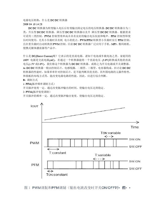
B:调制方式1: PFM(脉冲频率调制方式)开关脉冲宽度一定,通过改变脉冲输出的时间,使输出电压达到稳定。
2: PWM(脉冲宽度调制)开关脉冲的频率一定,通过改变脉冲输出宽度,使输出电压达到稳定。
C:通常情况下,采用PFM和PWM这两种不同调制方式的DC/DC转换器的性能不同点如下。
** PWM的频率,PFM的占空比的选择方法。
* PWM调制方式在选用较高频率的情况下(如:500KHz)(1)小负载时,效率很低。
(2)输出电压的纹波较小。
在选用较低频率的情况下(如:100KHz)(1)小负载时,效率较高。
(2)输出电压的纹波较大。
因此,在小负载或待机时间较长的情况下,选用100KHz的频率,转换电路的效率较高,但若考虑输出电压的纹波问题,若选用500KHz的频率,纹波电压会较小。
MIC23150 2A 4MHz 轻量级加载模式降压电源参考手册说明书
MIC23150 Evaluation Board4MHz 2A Buck Regulator withHyperLight Load™HyperLight Load is a trademark of Micrel, Inc. MLF is a registered trademark of Amkor Technology.Micrel Inc. • 2180 Fortune Drive • San Jose, CA 95131 • USA • tel +1 (408) 944-0800 • fax + 1 (408) 474-1000 • General DescriptionThe MIC23150 is a 2A 4MHz switching regulator featuring HyperLight Load™ mode. The MIC23150 is highly efficient throughout the entire output current range, drawing just 23µA of quiescent current in operation. The tiny 2mm x2mm MLF ®package, in combination with the 4MHz switching frequency, enables a compact sub-1mm height solution with only three external components. The MIC23150 provides accurate output voltage regulation under the most demanding conditions and responds extremely quickly to a load transient with exceptionally small output voltage ripple.Factoring in the output current, the internal circuitry of the MIC23150 automatically selects between two modes of operation for optimum efficiency. Under light load conditions, the MIC23150 goes into HyperLight Load™mode. HyperLight Load™ uses a Pulse-Frequency Modulation (PFM) control scheme that controls the off time at light load. This proprietary architecture reduces the amount of switching needed at light load, thereby increasing operating efficiency. The MIC23150 attains up to 87% efficiency at 1mA output load. As the load current increases beyond approximately 100mA, the device operates using the Pulse-Width Modulation (PWM) method for up to 93% efficiency at higher load. The two modes of operation ensure the highest efficiency across the entire load range.The MIC23150 operates from an input voltage range of 2.7V to 5.5V and features internal power MOSFETs that deliver up to 2A of output current. This step-down regulator provides an output voltage accuracy of +/-2.5% across the junction temperature range of -40ºC to +125ºC. The MIC23150 is available in fixed output versions supporting an output voltage as low as 1.0V.RequirementsThe MIC23150 evaluation board requires an input power source that is able to deliver greater than 2A at 2.7V to the MIC23150. The output load can either be an active (electronic) or passive (resistive) load.Getting Started1. Connect an external supply to the V IN (J1)terminal . Apply the desired input voltage to V IN (J1) and ground (J2) terminals of the evaluation board, paying careful attention to polarity and supply voltage (2.7V ≤ V IN ≤ 5.5V). An ammeter may be placed between the input supply and the V IN (J1) terminal. Be sure to monitor the supply voltage at the V IN (J1) terminal, since the ammeter and/or power lead resistance can reduce the voltage supplied to the device.2. Connect a load to the V OUT (J3) and groundterminal (J4). The load can be either passive (resistive) or active (electronic load). An ammeter may be placed between the load and the output terminal. Ensure the output voltage is monitored at the V OUT (J3) terminal.3. Enable the MIC23150. The MIC23150 evaluationboard has a pull-up resistor to V IN . To disable the device, apply a voltage below 0.5V to the EN (J5)terminal. In the absence of the pull-up resistor, the device is enabled by applying a voltage greater than 1.2V to the EN (J5) terminal. The enable pin must be either pulled high or low for proper operation. Removing the pull-up resistor and leaving the pin floating will cause the regulator to operate in an unknown state.Output VoltageThe MIC23150 evaluation board is available with the following output voltage options listed below:Ordering InformationPart Number Description(2)MIC23150-CYMT EV (1) 1.0V Fixed Output Evaluation Board MIC23150-4YMT EV(1)1.2V Fixed Output Evaluation Board MIC23150-GYMT EV 1.8V Fixed Output Evaluation Board MIC23150-SYMT EV3.3V Fixed Output Evaluation BoardNote:1. Contact Micrel Marketing2. Other voltage options available on request. Contact Micrel.HyperLight Load™ ModeMIC23150 uses a minimum on and off time proprietary control loop (patented by Micrel). When the output voltage falls below the regulation threshold, the error comparator begins a switching cycle that turns the PMOS on and keeps it on for the duration of the minimum-on-time. This increases the output voltage. If the output voltage is over the regulation threshold, then the error comparator turns the PMOS off for a minimum-off-time until the output drops below the threshold. The NMOS acts as an ideal rectifier that conducts when the PMOS is off. Using a NMOS switch instead of a diode allows for lower voltage drop across the switching device when it is on. The asynchronous switching combination between the PMOS and the NMOS allows the control loop to work in discontinuous mode for light load operations. In discontinuous mode, the MIC23150 works in pulse frequency modulation (PFM) to regulate the output. As the output current increases, the off-time decreases, thus provides more energy to the output. This switching scheme improves the efficiency of MIC23150 during light load currents by only switching when it is needed. As the load current increases, the MIC23150 goes into continuous conduction mode (CCM) and switches at a frequency centered at 4MHz. The equation to calculate the load when the MIC23150 goes into continuous conduction mode may be approximated by the following formula:˜˜¯ˆÁÁËÊ¥¥->f L D V V I OUT IN LOAD 2)(As shown in the previous equation, the load at which MIC23150 transitions from HyperLight Load™ mode to PWM mode is a function of the input voltage (V IN ), output voltage (V OUT ), duty cycle (D), inductance (L) and frequency (f). As shown in Figure 1, as the Output Current increases, the switching frequency also increases until theMIC23150 goes from HyperLight Load TMmode to PWM mode at approximately 120mA. The MIC23150 will switch at a relatively constant frequency around 4MHz once the output current is over 120mA.Figure 1. SW Frequency vs. Output CurrentMIC23150 Typical Application CircuitBill of MaterialsItem Part Number Manufacturer Description Qty. C1, C2C1608X5R0J475K TDK(1) 4.7µF Ceramic Capacitor, 6.3V, X5R, Size 06032 R1CRCW06031002K0FKEA Vishay(2)10kΩ, 1%, Size 06031 VLS3010T-1R0N1R9TDK(1)1µH, 1.9A, 60mΩ, L3.0mm x W3.0mm x H1.0mm1 L1VLS4012T-1R0N1R6TDK(1)1µH, 2.8A, 50mΩ, L4.0mm x W4.0mm x H1.2mmDO2010-102ML Coilcraft(3)1µH, 1.8A, 162mΩ, L2.0mm x W2.0mm x H1.0mm U1MIC23150-xYMT Micrel, Inc.(4)4MHz 2A Buck Regulator with HyperLight Load™ Mode1 Notes:1. TDK: .2. Vishay: .3. Coilcraft: .4. Micrel, Inc.: .PCB Layout RecommendationsTop LayerBottom Layer。
IR3621MTRPBF资料
IR3621 & (PbF)Data Sheet No.PD60231 revAIR3621 & (PbF)IR3621 & (PbF)ELECTRICAL SPECIFICATIONSUnless otherwise specified, these specifications apply over Vcc=12V, VcH1=VcH2=V CL =12V and 0°C<T j <125°C.PARAMETERSYMBOL TEST CONDITIONMIN TYP MAX UNITSOutput Voltage Accuracy Feedback VoltageAccuracyUVLO SectionUVLO Threshold - Vcc UVLO Hysteresis - VccUVLO Threshold - VcH1,2UVLO Hysteresis - VcH1,2Supply Current Section Vcc Dynamic Supply Current VcH1 & VcH2 Dynamic Current V CL Dynamic Supply Current Vcc Static Supply Current VcH1/VcH2 Static Current V CL Static Supply Current MLPQTSSOPSupply Ramping UpSupply Ramp Up and Down Supply Ramping UpSupply Ramp Up and Down Freq=300kHz, C L =1500pF Freq=300kHz, C L =1500pF Freq=300kHz, C L =1500pFSS=0V SS=0V SS=0V 0.8010.751015151066V %%%%%%V V V V mA mA mA mA mA mA V Fb1 , V Fb2UVLO V CC UVLO V C H1,2Dyn I CC Dyn I CH Dyn I CL I CCQI CHQI CLQ-1-1.35 -2.5-1.35-1.65-3.04.73.5+1+1.35+1.35+1.35+1.65+1.655.34.0152525151010280.9V REF 0.1-0.110001.25300µA V V V µA µmho µmho µA mV V kHz V %ns %kHz ns V VSS IB SD PG FB1,2L PG (Voltage)I FB1,2g m1g m2I (E/A)1,2V OS(ERR)VP2Freq V RAMP Dmin Puls(ctrl)Dmax Sync(Fs)Sync(puls)Sync(H)Sync(L)220.8V REF 1400140060-40.425515086.52002350.250.95V REF0.5-0.525002500140+4Vcc-234512000.6Soft-Start / SD SectionCharge CurrentShutdown ThresholdPower Good SectionV SENS1,2 Lower Trip PointPGood Output Low VoltageError Amp SectionFb Voltage Input Bias CurrentTransconductance 1Transconductance 2Error Amp Source/Sink CurrentInput Offset Voltage for E/A1,2VP2 Voltage RangeOscillator SectionFrequencyRamp AmplitudeMin Duty CycleMin Pulse WidthMax Duty CycleSynch Frequency RangeSynch Pulse DurationSynch High Level ThresholdSynch Low Level ThresholdSS=0V V SENS1,2 Ramping Down I SINK =2mA SS=3V Fb 1,2 to V REF Note2Rt (SET) to 30.9K Note2Fb=1V F SW =300kHz, Note2Fb=0.6V, F SW =200kHz 20% above free running freq Note1: Cold temperature performance is guaranteed via correlation using statistical quality control. Not 100% tested in production.Tj=25°C-40°C <T j < 125°C 0°C <T j < 125°C 0°C <T j < 125°C -40°C <T j < 125°CTj=25°CIR3621 & (PbF)IR3621 & (PbF)PIN DESCRIPTIONS 12345,236,227,218209,1910,1811,1712,1613,15142425262728Power Good pin. Low when any of the outputs fall 10% below the set voltages. Supply voltage for the internal blocks of the IC. The Vcc slew rate should be <0.1V/us.Output of the internal LDO. Connect a 1.0uF capacitor from this pin to ground. Connecting a resistor from this pin to ground sets the oscillator frequency. Sense pins for OVP and PGood. For current share tie these pins together. Inverting inputs to the error amplifiers. In current sharing mode, Fb1 is con-nected to a resistor divider to set the output voltage and Fb2 is connected to programming resistor to achieve current sharing. In independent 2-channel mode, these pins work as feedback inputs for each channel.Compensation pins for the error amplifiers.These pins provide user programmable soft-start function for each outputs. Connect external capacitors from these pins to ground to set the start up time for each output. These outputs can be shutdown independently by pulling the respective pins below 0.3V. During shutdown both MOSFETs will be turned off. For current share mode SS2 must be floating.A resistor from these pins to switching point will set current limit threshold. Supply voltage for the high side output drivers. These are connected to voltages that must be typically 6V higher than their bus voltages. A 0.1µF high fre-quency capacitor must be connected from these pins to PGND to provide peak drive current capability.Output drivers for the high side power MOSFETs. Note3These pins serve as the separate grounds for MOSFET drivers and should be connected to the system’s ground plane.Output drivers for the synchronous power MOSFETs.Supply voltage for the low side output drivers.The internal oscillator can be synchronized to an external clock via this pin. When pulled High, it puts the device current limit into a hiccup mode. When pulled Low, the output latches off, after an overcurrent event.Non-inverting input to the second error amplifier. In the current sharing mode, it is connected to the programming resistor to achieve current sharing. In inde-pendent 2-channel mode it is connected to V REF pin when Fb2 is connected to the resistor divider to set the output voltage.Reference Voltage. The drive capability of this pin is about 2µA.Analog ground for internal reference and control circuitry.TSSOP MLPQ PIN SYMBOL PIN DESCRIPTION2930311 2,22 3,21 4,20519 6,18 7,17 8,16 10,14 11,13122324262728 9,15,25.32PGoodVccV OUT3RtV SEN2, V SEN1Fb2,Fb1 Comp2, Comp1 SS2 / SDSS1 / SD OCSet2,OCSet1 VcH2, VcH1 HDrv2, HDrv1 PGnd2, PGnd1 LDrv2, LDrv1V CLSyncHiccupV P2V REFGndN/CNote3: The negative voltage at these pins may cause instability for the gate drive circuits. T o prevent this, a low forward voltage drop diode (Schottky) is required between these pins and power ground.No ConnectIR3621 & (PbF)IR3621 & (PbF)Figure 5 - 30A Current Sharing using Inductor sensing(5A/Div)IR3621 & (PbF)IR3621 & (PbF)IR3621 & (PbF)IR3621 & (PbF)IR3621 & (PbF)For higher efficiency, low ESR capacitors are recom-mended.Choose two Poscap from Sanyo 16TPB47M (16V, 47µF ,70m Ω ) with a maximum allowable ripple current of 1.4A for inputs of each channel.Inductor SelectionThe inductor is selected based on operating frequency,transient performance and allowable output voltage ripple.Low inductor values result in faster response to step load (high ∆i/∆t) and smaller size but will cause larger output ripple due to increased inductor ripple current. As a rule of thumb, select an inductor that produces a ripple current of 10-40% of full load DC.For the buck converter, the inductor value for desired operating ripple current can be determined using the fol-lowing relation:V IN - V OUT = L × ; ∆t = D × ; D =1f SV OUT V IN ∆i ∆t L = (V IN - V OUT )× ---(7)V OUTV IN ×∆i ×f SWhere:V IN = Maximum Input Voltage V OUT = Output Voltage∆i = Inductor Ripple Current f S = Switching Frequency ∆t = Turn On Time D = Duty CycleWhere:∆V O = Output Voltage Ripple ∆i = Inductor Ripple Current∆V O = 3% of V O will result to ESR (2.5V) =16.6m Ω and ESR (1.8V) =16m ΩESR ≤ ---(8)∆V O∆I OThe Sanyo TPC series, Poscap capacitor is a good choice.The 6TPC330M, 330µF, 6.3V has an ESR 40m Ω. Se-lecting three of these capacitors in parallel for 2.5V out-put, results to an ESR of ≅ 13.3m Ω which achieves our low ESR goal. And selecting three of these capacitors in parallel for 1.8V output, results in an ESR of ≅ 13.3m Ωwhich achieves our low ESR goal.The capacitors value must be high enough to absorb the inductor's ripple current.Power MOSFET SelectionThe IR3621 uses four N-Channel MOSFETs. The selec-tion criteria to meet power transfer requirements is based on maximum drain-source voltage (V DSS ), gate-source drive voltage (V GS ), maximum output current, On-resis-tance R DS(ON) and thermal management.The both control and synchronous MOSFETs must have a maximum operating voltage (V DSS ) that exceeds the maximum input voltage (V IN ).Input Capacitor SelectionThe 1800 out of phase will reduce the RMS value of the ripple current seen by input capacitors. This reduces numbers of input capacitors. The input capacitors must be selected that can handle both the maximum ripple RMS at highest ambient temperature as well as the maximum input voltage. The RMS value of current ripple for duty cycles under 50% is expressed by: For ∆i (2.5V) = 45%(I O(2.5V) ), then the output inductor will be:L 4 = 1.1µHFor ∆i (1.8V) = 35%(I O(1.8V) ), then the output inductor will be:L 3 = 1.1µH Panasonic provides a range of inductors in different val-ues and low profile for large currents.Output Capacitor SelectionThe criteria to select the output capacitor is normally based on the value of the Effective Series Resistance (ESR). In general, the output capacitor must have low enough ESR to meet output ripple and load transient requirements, yet have high enough ESR to satisfy sta-bility requirements. The ESR of the output capacitor is calculated by the following relationship: I RMS = (I 12D 1(1-D 1)+I 22D 2(1-D 2)-2I 1I 2D 1D 2) --- (6)Where:I RMS is the RMS value of the input capacitor current D 1 and D 2 are the duty cycle for each output I 1 and I 2 are the current for each output For this application the I RMS =4.8A(ESL, Equivalent Series Inductance is neglected)Choose ETQP6F1R1BFA (1.1µH, 16A, 2.2m Ω) both for L 3 and L 4.For 2-phase application, equation (7) can be used for calculating the inductors value. In such case the induc-tor ripple current is usually chosen to be between 10-40% of maximum phase current.The gate drive requirement is almost the same for both MOSFETs. Logic-level transistors can be used and cau-tion should be taken with devices at very low Vvent undesired turn-on of the complementary MOSFET which results in a shoot-through.IR3621 & (PbF)IR3621 & (PbF)IR3621 & (PbF)IR3621 & (PbF)IR3621 & (PbF)IR3621 & (PbF)IR3621 & (PbF)IR3621 & (PbF)IR3621 & (PbF)TYPICAL OPERATING WAVEFORMSTest Conditions:V IN=12V, V OUT1=2.5V, I OUT1=0-10A, V OUT2=1.8V, I OUT2=0-10A, Fs=400kHz, T A=Room Temp, No Air Flow Unless otherwise specified.Figure 21 - Start up waveforms for 2.5V output Ch1: Vin, Ch2: Vout3, Ch3: SS1, Ch4:Vo1 (2.5V)Figure 22 - Start up waveforms for 1.8V output Ch1: Vin, Ch2: Vout3, Ch3: SS2, Ch4:Vo2 (1.8V)Figure 23 - Start up waveforms Ch1: Vin, Ch2: Vout3, Ch3: VrefFigure 24 - Vo1, Vo2 and PGoodCh1: Vin, Ch2: Vo1, Ch3: Vo2, Ch4: PGoodIR3621 & (PbF)TYPICAL OPERATING WAVEFORMSTest Conditions:V IN =12V, V OUT1=2.5V, I OUT1=0-10A, V OUT2=1.8V, I OUT2=0-10A, Fs=400kHz, Ta=Room Temp, No Air FlowUnless otherwise specified.Figure 25 - 2.5V outputCh1: Vin, Ch2: SS1, Ch3: Vo1, Ch4: PGoodFigure 26 - 1.8V outputCh1: Vin, Ch2: SS2, Ch3: Vo2, Ch4: PGoodFigure 27 - Gate waveforms with 180oout of phaseCh1: Hdrv1, Ch2: Hdrv2Figure 28 - 2.5V WaveformsCh1: Hdrv1, Ch2: Ldrv1, Ch3: Lx1, Ch4: Inductor CurrentIR3621 & (PbF)Figure 29 - 2.5V WaveformsCh1: Hdrv2, Ch2: Ldrv2, Ch3: Lx2, Ch4: Inductor Current Figure 30 - 1.8V output shortedCh1: Vo1, Ch2: SS2, Ch3: Inductor CurrentFigure 31 - 2.5V output shortedCh1: Vo2, Ch2: SS1, Ch3: Inductor CurrentFigure 32 - Prebias Start upCh1: SS1, Ch2: Vo1, Ch3: SS2, Ch4:Vo2TYPICAL OPERATING WAVEFORMSTest Conditions:V IN =12V, V OUT1=2.5V, I OUT1=0-10A, V OUT2=1.8V, I OUT2=0-10A, Fs=400kHz, Ta=Room Temp, No Air Flow Unless otherwise specified.IR3621 & (PbF)Figure 33 - SS1 pin shorted to GndCh1: SS1, Ch2: Hdrv1, Ch3: Ldrv1, Ch4:Vo2Figure 34 - SS2 pin shorted to GndCh1: SS2, Ch2: Hdrv2, Ch3: Ldrv2, Ch4:Vo1Figure 35 - External Synchronization Ch1: External Clock, Ch2: Hdrv1, Ch3: Hdrv2TYPICAL OPERATING WAVEFORMSTest Conditions:V IN =12V, V OUT1=2.5V, I OUT1=0-10A, V OUT2=1.8V, I OUT2=0-10A, Fs=400kHz, Ta=Room Temp, No Air Flow Unless otherwise specified.IR3621 & (PbF)TYPICAL OPERATING WAVEFORMSTest Conditions:V IN =12V, V OUT1=2.5V, I OUT1=0-10A, V OUT2=1.8V, I OUT2=0-10A, Fs=400kHz, Ta=Room Temp, No Air FlowUnless otherwise specified.Figure 36 - Load Transient Respons for Vo1(Io=0 to 10A)Ch1: Vo1, Ch4:Io1Figure 37 - Load Transient Respons for Vo1(Io=10 to 0A)Ch1: Vo1, Ch4: Io1Figure 39 - Load Transient Respons for Vo2(Io=10 to 0A)Ch1: Vo2, Ch4: Io2Figure 38 - Load Transient Respons for Vo2(Io=0 to 10A)Ch1: Vo2, Ch4: Io2IR3621 & (PbF)IR3621 & (PbF)IR3621 & (PbF)。
TI UC1715-SP 互补型开关驱动器说明书
W PACKAGEUC1715-SP ZHCSAU7–MAY2013互补型开关场效应晶体管(FET)驱动器查询样品:UC1715-SP特性•单输入(脉宽调制(PWM)和晶体管-晶体管逻辑电路(TTL)兼容)•高电流功率FET驱动器,1A拉电流/2A灌电流•辅助输出FET驱动器,0.5A拉电流/1A灌电流•电源与独立可编程辅助输出间的时间延迟范围50ns至700ns•针对每个输出可单独配置时间延迟或真正零电压运行•开关频率达到1MHz•典型值为50ns的传播延迟•ENBL引脚激活220μA睡眠模式•睡眠模式中电源输出低电平有效•同步整流器驱动器说明UC1715是一款被设计成为互补型开关提供驱动波形的高速驱动器。
互补型开关配置通常用于同步整流电路和有源钳位/复位电路,它可提供零电压切换。
为了便捷软开关转换,这个驱动器提供两个输出波形间的独立可编程延迟。
此延迟引脚还具有真正零电压感测功能,这个功能可在采用零电压时实现相应开关的立即激活。
这个器件的运行需要一个PWM类型输入,而且此器件可与常见的PWM控制器对接。
ORDERING INFORMATION(1)T J PACKAGE ORDERABLE PART NUMBER TOP-SIDE MARKING –55°C to125°C CFP(W)5962-0052102VFA5962-0052102VFA(1)For the most current package and ordering information,see the Package Option Addendum at the end of this document,or see the TIweb site at .Please be aware that an important notice concerning availability,standard warranty,and use in critical applications ofTexas Instruments semiconductor products and disclaimers thereto appears at the end of this data sheet.UC1715-SPZHCSAU7–DEVICE INFORMATIONPIN FUNCTIONSPINI/O DESCRIPTIONNAME NO.1,7,8,N/C9,10,-N/C pins are not bonded out.External connections will not affect device functionality.12,13The V CC input range is from7V to20V.This pin should be bypassed with a capacitor to GND consistent with V CC2Ipeak load current demands.The PWR output waits for the T1delay after the INPUT’s rising edge before switching on,but switches offimmediately at INPUT’s falling edge(neglecting propagation delays).This output is capable of sourcing1-A PWR3Oand sinking2-A of peak gate drive current.PWR output includes a passive,self-biased circuit which holds thispin active low,when ENBL≥0.8V regardless of VCC’s voltage.This is the reference pin for all input voltages and the return point for all device currents.It carries the full GND4,5-peak sinking current from the outputs.Any tendency for the outputs to ring below GND voltage must bedamped or clamped such that GND remains the most negative potential.The AUX switches immediately at INPUT’s rising edge but waits through the T2delay after INPUT’s falling AUX6edge before switching.AUX is capable of sourcing0.5-A and sinking1-A of drive current.During sleep mode, AUX is inactive with a high impedance.This pin functions in the same way as T1but controls the time delay between PWR turn-off and activation ofthe AUX switch.The resistor on this pin sets the charging current on internal timing capacitors to provide independent timecontrol.The nominal voltage level at this pin is3V and the current is internally limited to1mA.The total delay T211from INPUT to output includes a propagation delay in addition to the programmable timer but since thepropagation delays are approximately equal,the relative time delay between the two outputs can be assumedto be solely a function of the programmed delays.The relationship of the time delay vs.RT is shown in theTypical Characteristics curves.The input switches at TTL logic levels(approximately1.4V)but the allowable range is from0V to20V,allowing direct connection to most common IC PWM controller outputs.The rising edge immediately switchesthe AUX output,and initiates a timing delay,T1,before switching on the PWR output.Similarly,the INPUTfalling edge immediately turns off the PWR output and initiates a timing delay,T2,before switching the AUX INPUT14Ioutput.It should be noted that if the input signal comes from a controller with FET drive capability,this signal providesanother option.INPUT and PWR provide a delay only at the leading edge while INPUT and AUX provide thedelay at the trailing edge.A resistor to ground programs the time delay between AUX switch turn-off and PWR turn-on.The resistor on this pin sets the charging current on internal timing capacitors to provide independent timecontrol.The nominal voltage level at this pin is3V and the current is internally limited to1mA.The total delay T115from INPUT to output includes a propagation delay in addition to the programmable timer but since thepropagation delays are approximately equal,the relative time delay between the two outputs can be assumedto be solely a function of the programmed delays.The relationship of the time delay vs.RT is shown in theTypical Characteristics curves.The ENBL input switches at TTL logic levels(approximately1.2V),and its input range is from0V to20V. ENBL16I The ENBL input will place the device into sleep mode when it is a logical low.The current into VCC during the sleep mode is typically220μA.INPUTT1T2 ENBLAUXPWRVCCGND UC1715-SP ZHCSAU7–MAY2013BLOCK DIAGRAMABSOLUTE MAXIMUM RATINGS(1)(2)over operating free-air temperature range(unless otherwise noted)V CC Supply voltage20VContinuous-100mA Power driverPeak(3)-1AI OHContinuous-100mA Auxiliary driverPeak(3)-500mAContinuous100mA Power driverPeak(3)2AI OLContinuous100mA Auxiliary driverPeak(3)1AV I Input voltage range(INPUT,ENBL)–0.3V to20VT J Maximum operating junction temperature150°CT stg Storage temperature range–65°C to150°CT lead Maximum lead temperature(soldering,10seconds)300°C(1)Stresses beyond those listed under absolute maximum ratings may cause permanent damage to the device.These are stress ratingsonly,and functional operation of the device at these or any other conditions beyond those indicated under recommended operating conditions is not implied.Exposure to absolute-maximum-rated conditions for extended periods may affect device reliability.(2)All voltages are with respect to ground.Currents are positive into,negative out of the specified terminal.(3)RMS drive current on any pin to be restricted to672mA.UC1715-SPZHCSAU7–THERMAL INFORMATIONUC1715-SPTHERMAL METRIC(1)W UNITS16PINSθJA Junction-to-ambient thermal resistance(2)72.9θJC Junction-to-case thermal resistance(3)8.25°C/WθJB Junction-to-board thermal resistance(4)43.4(1)有关传统和新的热度量的更多信息,请参阅IC封装热度量应用报告,SPRA953。
dq轴电压与直流侧电压关系
dq轴电压与直流侧电压关系直流(Direct Current,简称DC)电压是指电流方向不变的电压信号。
它是通过在一个电源中产生直流电流,并在电路中保持恒定的电压。
在直流电压源的引导下,产生出的电流在电路中向一个方向流动。
与直流电流相对,交流(Alternating Current,简称AC)电压是指电流方向周期性变化的电压信号。
交流电压是由发电机、变压器等电源产生的,其电流按照一定的频率无规律地在正负方向之间来回变化。
在工程实践中,有时需要将交流电压转化为直流电压以供电路中的某些元器件使用。
为此,我们需要使用交流与直流之间的电力转换方式。
其中,一种常用的转换方式是使用电力电子器件实现直流电压的获取和整流。
使用电力电子器件来实现直流电压的获取,其中最常见的方式是使用直流电压源与交流电源相连接,通过电器设备将交流电源经过整流、滤波和调整电压等处理步骤得到直流电压。
电力电子器件常用的有整流二极管、整流桥、磁阻器、电容器等。
对于由直流电压源提供的直流电压,其电压幅值是恒定的,不随时间变化。
而对于由交流电压源产生的交流电压,其幅值大小和信号的频率有关。
在实际应用中,为了满足电路的需要,可能需要对直流电压进行调节或变换。
这时,可以使用变压器、稳压二极管、开关电源等电器设备对直流电压进行调整。
变压器是一种常用的电力转换设备,在电路中用来改变电压的大小。
它通过改变绕组的匝数比例来改变输入和输出的电压。
变压器能够使电压升高或降低,但频率不会变化。
稳压二极管也是一种常用的电子设备,可以将输入的直流电压稳定在一定的范围内。
开关电源是一种将交流电转换成直流电的高效率电源。
它通过开关电子器件的转换来实现电能的转化和调整。
开关电源可以根据需要,通过控制开关器件的开合来调整输出电压的大小。
总之,在电路中,直流电压与直流电源、交流电压与交流电源之间存在一定的关系。
直流电压可以通过交流电压转换而来,而交流电压也可以通过相应的设备转换成直流电压。
- 1、下载文档前请自行甄别文档内容的完整性,平台不提供额外的编辑、内容补充、找答案等附加服务。
- 2、"仅部分预览"的文档,不可在线预览部分如存在完整性等问题,可反馈申请退款(可完整预览的文档不适用该条件!)。
- 3、如文档侵犯您的权益,请联系客服反馈,我们会尽快为您处理(人工客服工作时间:9:00-18:30)。
Direct current voltage induced by microwave signal in a ferromagnetic wireA.Yamaguchi1, K. Motoi1, H. Miyajima1, and Y. Nakatani21Department of Physics, Keio University, Hiyoshi 3-14-1, Yokohama, Kanagawa 223-8522, Japan2University of Electro-communications, Chofugaoka 1-5-1, Chofu, Tokyo 182-8585, Japan[ABSTRACT]Experimental results of rectification of a constant wave radio frequency (RF) current flowing in a single-layered ferromagnetic wire are presented. We show that a detailed external magnetic field dependence of the RF current induced a direct-current voltage spectrum. The mechanism of the rectification is discussed in a term of the spin transfer torque, and the rectification is closely related to resonant spin wave excitation with the assistant of the spin-polarized RF current. The micromagnetic simulation taking into account the spin transfer torque provides strong evidence which supports the generation of spin wave excitation by the RF current.I. INTRODUCTIONRecently it is found that the spin and electric charge of electrons in nano-artificial magnetic systems exhibit peculiar behaviors in the radio-frequency (RF) region through ferromagnetic resonance (FMR) which has led to the spin-polarized current in the RF region. Furthermore, spin wave excitation and magnetization reversal is induced by the spin-polarized RF current. From the view points of fundamental nano-scale magnetism and technical spintronics, many theoretical [1, 2] and experimental [3 - 16] studies have been progressed and focused on a system with spatial distribution of magnetization such as magnetic multilayers [3 – 10], magnetic tunnel junctions (MTJ) [11], spin-valves [12], and single-layered ferromagnetic wires [13 – 15]. These systems have numerous possible technical applications in magnetoresistive random access memory (MRAM), microwave generators [9, 10], and so on. The physical mechanism, as revealed by the experimental results, is described in term of the spin angular momentum transferring which occurs due to the interaction between the spin-polarized current and the magnetic moment. One of the most interesting properties is the rectification of RF current. When the resonant RF current flows through a system with magnetization distribution, it resonantly excites spin wave in the system and the magnetic moment precesses around the effective magnetic field consisting of magnetic anisotropy field, demagnetizing field and external field. As a result, the direct-current (DC) voltage is produced by the magnetoresistance oscillation due to FMR generated by the spin-transfer effect or RF field [11 - 19].In the previous studies of pillar structure systems consisting of two ferromagnetic layers (a spin-polarizer layer and a free layer) have been adopted to originate the spin-transfer effect. On the other hand, it has been clarified that the spin dynamics is excited by the spin- transfer torque due to the spin-polarized current flowing through a system with domain wall ormagnetic vortex core [13 - 16].In this paper, we present detail experimental results of the rectifying effect observed in a single-layered ferromagnetic nanowire [13]. As mentioned above, the rectifying effect is attributable to the resonant excitation of spin waves by the RF current. ()01cos I t I t ω=at time t . Once the spin wave is excited in the wire, the magnetic moment precesses around the effective magnetic field with the angular frequency ω1, the resistance change ∆R (t ) will oscillate as a function of 2cos ωt , originating from the anisotropic magnetoresistance (AMR) effect. The DC voltage given by ()()()V t I t R t =⋅∆ is generated by a term involving mixing between RF current and magnetoresistance;()()()01212cos cos 2V t V t t ωωωω⎡⎤=−++⎣⎦(1) If 12ωωω==, ()()01cos 2V t V t ω=+; that is, the nanowire acts as a detector which turns the RF signal to DC voltage with second harmonic oscillation.II. RECTIFYING EFFECT OF RF CURRENTWe focus on a single layered Ni 81Fe 19 wires [Fig. 1]. The wires are fabricated on MgO substrates using the procedure described in Ref. 13. We examine 30 and 50-nm-thick Ni 81Fe 19 nanowires and a 20-nm-thick Au nanowire contacted with Au electrode, of the 100 nm thick, as shown in Fig. 1. The width of the 50-nm-thick Ni 81Fe 19 nanowires is 300, 650, and 2200 nm and that of 30-nm-thick Ni 81Fe 19 and Au nanowires is 5 µm and 300 nm, respectively.A ground-signal-ground (GSG) type microwave prove is connected to the nanowire, and the bias-tee circuit detects the DC voltage difference induced by the RF current flowing through the nanowire, as schematically illustrated in Fig. 1. The sinusoidal constant wave RF current is injected into the nanowire by a signal generator with a frequency range from 10 MHz to 40 GHz. The external magnetic field ext H is applied in the substrate plane as a function of angle θ to the longitudinal axis of the nanowire, while the Oersted field produced by the RF currents flowing in the loop of the Au electrodes generates an additional field at the sample. However, the field is canceled out at the nanowire position because of the symmetrical arrangement of the Au electrode. All experiments are performed at room temperature.Figure 5 shows the magnetic field dependence of the DC voltage difference generated in the wires with widths of 5 µm. The RF current density injected into the wire is about 102.310×A/m 2, the value of which is relatively low for the Joule heating to be applied. According to our recent estimation of the current density from the measurement of the RF characteristic impedance of the wire, the density is found to be almost same to the value. An external magnetic field is applied in the substrate plane at the angle of (a) 0D , (b) 30D , (c) 60D , and (d) 90D to the wire-axis. As seen in the figure, the peak position of resonance spectrum shifts to the higher frequency region with the external magnetic field. The sign of the DC voltage reverses when the angle of the applied magnetic field is changed form θ to180θ+D . On the other hand, no similar effects are observed in the 20-nm-thick Au nanowires, which strongly indicates that the resonance is of magnetic origin and generated by the RF current.Figure 3 shows the magnetic field dependence of the resonance frequency of the nanowire with widths of 300, 650, 2200, and 5000 nm, where the magnetic field is applied at the angle of D 45 to the wire-axis. The resonance frequency increases with increasing magnetic field but decreasing wire-width, which means that the resonance mode possibly reflects the shape magnetic anisotropy.According to the extended Kittel’s equation [20], the ferromagnetic resonance frequency at the magnetic field H is approximately given by()()102()B A S A g H H H M H H µµω⎡⎤=⋅++⋅+⎣⎦=, (2)where M S denotes the saturation magnetization, g the Lande factor, = Planck’s constant, µ0 the permeability of free space, B µ the Bohr magneton, and A H the effective anisotropy field including demagnetizing and anisotropy fields in the substrate plane. The experimentally determined A H for the nanowires with widths of 300, 650, 2200, and 5000 nm is 1160, 830, 260, and 100 Oe, respectively. The resonance frequency is in excellent agreement with that of calculation using the extended Kittel’s eq.(2), indicating the existence of resonant spin wave excitation. As the RF current induces the precession of the magnetic moments in the nanowiresand the excitation of the spin wave, the resistance due to the AMR effect oscillates at the resonance frequency. This resistance oscillation generates the DC voltage by combining with the RF current, as observed in the case of the spin-torque diode effect in the pillar structure systems [11, 12].III. MICROMAGNETICS CALCULATIONThe current-induced dynamics of the magnetic moment are analytically calculated by the micromagnetic simulations based on the Landau-Lifshitz-Gilbert (LLG) equation including the spin-transfer term [16, 21]. The modified LLG equation is given by()0eff s t t γα∂∂=−×+×−⋅∇∂∂mm m H m u m , (3) where m denotes the unit vector along the local magnetization, 0γ the gyromagnetic ratio, eff H the effective magnetic field including the exchange and demagnetizing fields, and α the Gilbert damping constant, respectively. The last term in eq. (3) represents the spin-transfer torque which describes the spin transferred from conduction electrons to localized spins. The spin-transfer effect is a combined effect of the spatial non-uniformity of magnetization distribution and the current flowing. The vector with dimension of velocity, ()/2s B s Pg eM µ=−u j , is essentially the spin current associated with the electric current,where j is the current density, P the spin polarization of the current, and e theelectronic charge, respectively. The spatial non-uniformity of the magnetization distribution in a nanowireis mainly caused by the spatial dispersion of the demagnetizing field.A micromagnetic simulation of the system considering the spin transfer torque is performed to confirm the generation of spin wave excitation by the constant wave RF current[16, 21]. The nanowire adopted in the simulation has a width and length of 300 nm and 4 µm, respectively. The parameters used for the calculation are; the unit cell size of 4 nm × 4 nm with constant thickness 50 nm, the magnetization 1.08 T, the spin current density u = 3.25 m/s, and the spin polarization p = 0.7 [16]. In the simulation, the external magnetic field of 200 Oe is applied in the substrate plane at the angle of 45D from the wire-axis, where the magnitude of the field is not large enough to direct perfectly the magnetization along the direction of the applied magnetic field. The local spins in the nanowire are almost parallel to the effective anisotropy field.Figure 4 (a) shows a snapshot of the map and the cross-section of the z component of the magnetization in the middle of the simulation. The black and white stripes correspond to the –z and +z components of the magnetization, respectively, and the stripe magnetization pattern due to the spin wave excitation induced by the RF current is clearly observed. It should be noted that the period of the stripe pattern of approximately 100 nm is consistent with the spin wave length estimated byA and K are the exchange stiffness constant and the anisotropy energy written by K =0BC g H µµ, respectively. The magnetization response issimulated as a function of the RF current frequency. The mean values of the y and z components of magnetization are shown in Fig. 4 (b) as a function of the RF frequency. The mean value of x component is not suitable for the analysis as it has large background because of the uniaxial magnetic anisotropy. As shown in Fig. 4 (b), both y and z components peak at 10.4 GHz, which is consistent with the spin wave resonance frequency. The simulation result is in accord with the experimental result.IV . SIMPLE ANYLYTICAL MODEL AND EXPERIMENTAL RESULTHere, we derive an analytical expression for the DC voltage produced by the spin wave excitation. Suppose we have an (x , y , z ) coordinate system: each component corresponds to the short wire axis, longitudinal wire axis, and normal to the substrate plane,respectively, as schematically shown in Fig. 5 (a). The external magnetic field ext H isapplied along the angle θ fromthe y -coordinate axis. Then, let us define a new coordinate system (a , b , c ) where the b direction corresponds to the equilibrium direction of unit magnetization 0m along an effective magnetic field eff H including ext H and A H (the shape magnetic anisotropy field). The unit vector 0m inclines at an angle ψ to the y -coordinate axis, and A H is parallel to the y -coordinate axis. The magnetization precession around eff H only results in a small time-dependent component of the magnetization perpendicular to 0m . The assumption is valid whenever the spin wave excitation is small. Then, we decompose the unitvector m in the (a , b , c ) coordinate system as ()()0t t δ=+m m m , considering a small variation ()()(),0,a c m t m t δ=m and ()00,1,0=m . The vector m is obtained from eq.(3): 00eff t tδγα∂∂≈−×+×−∂∂m m H m s , (4) where(),,a b c m m m =m ,b m =, (5)and the spin transfer torques almost perpendicular to 0m in the (a , b , c ) coordinate systemis defined as ()()cos ,sin ,s a b c j s s s ψψ=⋅∇=⋅−s u m ,(6) The effective field eff H is expressed in the (a , b , c ) coordinate system as()()sin sin cos cos 00a ext A eff b ext A H H H H H H θψψθψψ−−⎛⎞⎛⎞⎜⎟⎜⎟==−+⎜⎟⎜⎟⎜⎟⎜⎟⎝⎠⎝⎠H .(7)Substituting eq. (5), (6), and (7) into eq. (3), we obtain the magnetization dynamics;0cos 0sin a c b c a b c a b c a b b a a c m m H m s m m H j s t t m m H m H m s ψγαψ−⎛⎞⎛⎞⎛⎞⎛⎞∂∂⎜⎟⎜⎟⎜⎟⎜⎟≈−+−−⎜⎟⎜⎟⎜⎟⎜⎟∂∂⎜⎟⎜⎟⎜⎟⎜⎟−−⎝⎠⎝⎠⎝⎠⎝⎠ (8) Under the conditions 1=m and 1b m ≈, eq. (8) is reduced to,0cos a c b c a c a b a a c m m H m s j m m H H m s t t ψγα−⎛⎞⎛⎞⎛⎞⎛⎞∂∂≈−+−⎜⎟⎜⎟⎜⎟⎜⎟−−∂∂⎝⎠⎝⎠⎝⎠⎝⎠, (9)assuming that the time-dependent magnetization precession angle around the direction of 0m is parallel to eff H and that the angle is very small. The solution of eq. (9) can bepresented by the Fourier transformation; ()()220cos 1k a a k c c a k i i m js i i m js H i ωωωαψωωαωγωωωα+⎛⎞⎛⎞⎛⎞=⎜⎟⎜⎟⎜⎟−+−−+⎝⎠⎝⎠⎝⎠, (10) where 0k b H ωγ= denotes the spin wave resonant angular frequency corresponding to ()H ω given by eq.(2).Due to the spin wave excitation with precession angle of l φ, the small variation in the magnetic moment around the direction of eff H induces the time-dependent AMR effect. When ()2cos 1l φ≈ and ()2sin 0l φ≈ for small l φ, we can approximately derive the average time-dependent resistance ()R t in each cell;()()()()221cos cos sin 2sin 22R t R t R t ∆ψφ∆ψψφ⎡⎤=+≈−⎢⎥⎣⎦∑AA A , (11) where ∆R denotes the resistance change due to the AMR effect, the number l the index of the domain of the spin wave excitation, and ()sin 22a φ∆≈A m m by using the a componentof δm . When the RF current given by ()()0cos I t I t ω= flows in the wire, the frequency spectrum of the induced voltage is expressed by the Fourier transformation of ()()()V t R t I t =;()()20sin 2cos V A I ωωψψ=,(12)where ()A ω is written by()()()()222102222222/cos 4k a k k c a k k s s H j R A b dωαωωωωγψωωωωαω−⋅+−⋅−∆≈⋅⋅−+, (13)where b and d are the width and thickness of the nanowire, respectively. In the case that ext H is higher than A H , the magnetic moment directs almost along ext eff ≈H H . Then, we obtain ψθ≈ ( see Fig. 5 (a)), which well corresponds to the result described in Ref 13. The relation ψθ≈ gives the frequency variation of the induced voltage ()V ω proportional to 20sin 2cos I θθ. On the contrary, ext H is smaller than A H , the magnetic moment is almost parallel to the direction of eff H . Then, 0const.ψθ<=<D , and the ()V ω is almost proportional to sin ext H θ. This means that the out-of-plane component of magnetization leads to the dispersion shape.As a result, the field and angle dependences of the induced DC voltage ()ωV are summarized as follows:(i)()θθωcos 2sin ∝V in ,ext A >>H H (ii) ()θωsin ext H V ∝in ext A <H HFigures 5 (b), (c), and (d) show the angle dependence of the induced DC voltage at the resonance frequency in the magnetic field of 400, 100, and 30 Oe, respectively. The inset of Fig.5 (b) shows the experimental result of the magnetoresistance for 30 nm-thick Ni 81Fe 19 wire with 5 µm width in the magnetic field perpendicular to the longitudinal wire axis(D 90=θ).The result of the magnetoresistance measurement in the inset of Fig. 5 (b) offersevidence that the magnetization is almost parallel to the direction of the field ext H at 400ext =H Oe. Then, according to the analytical model described above, the angle dependence of the induced DC voltage ()ωV should be proportional to θθcos 2sin , corresponding to the case (i). In Fig. 5 (b), the dashed-line represents the θθcos 2sin curve, and it is in good agreement with the experimental results. The magnetization is almost along the direction of A H at 30ext =H Oe. Then, the angle dependence of the induced DC voltage ()ωV corresponds to the case (ii), that is ()θωsin ext H V ∝. In Fig. 5 (d), the experimental result is consistent with the sin θ curve. As shown in Figs. 5 (b) and (d), we found that the simple analytical model expression given by eqs. (12) and (13) qualitatively fits well to the experimental results. The angle dependence of ()ωV at 100ext =H Oe is intermediate with the angle dependence between the cases (i) and (ii) as shown in Fig. 5 (c).The spectra shape is determined by ()A ω of eq. (13). ()A ω is given by the superposition of the Lozentzian function with a maximum at k ωω= and the dispersion function. The component of the Lozentzian function basically governs ()A ω, indicating that the in-plane spin transfer component determines the spectrum shape. However, as the angle θ increases, the component of the dispersion function in ()A ω increases. This is consistent with the actual spectra shapes observed in the experimental results shown in Fig. 2. The additional wiggles in the trace of Fig. 2 correspond to the additional spin wave modes derivedfrom the complicated spin wave excitation. While, if the in-plane RF field induce the magnetization dynamics, the spectrum shape is described only the dispersion function [19].The solution of eqs. (12) and (13) can be also represented as follows:()()sin 2cos V I R ωωψψ=⋅∆⋅Γ⋅, (14)()()()()222102222222cos 4k a k k c a k k js js H ωωαωωωγψωωωαωω−⋅+−⋅−Γ≈−+. (15)Here, ()ωΓ gives the dimensionless value and the spectrum shape. We can fit the change in the normalized DC voltage ()R I V ∆ω observed using the eq.(14). With the in-plane and the out-of-plane component of the spin transfer torque a js , c js , and the Gilbert damping parameter α as fit parameters, the typical signals measured in the wire with width of 5 µm in the application of the external field 400ext =H Oe could be fitted as shown in Fig. 6. These fits allow us to determine those parameters, which were found to be ()65,,(4.4510,6.7910,0.016)a c js js α=×× at 15θ=D and ()66,,(1.4510,3.1310,0.010)a c js js α=×× at 30θ=D in the wire with width of 5 µm. The Gilbert damping constants determined by the fittings agree with the values reported by Costache et al . [18], and they are larger than the value commonly accepted for a thin film of Ni 81Fe 19 [22]. In addition, we note here that the DC voltage spectrum shape, comprising of the superposition of the Lorentzian function and the dispersion function, changes to a more complex and wiggle shape as the frequency and angle applied external field change. These canbe due to the spatial inhomogeneities of the incoherent spin wave excitation and out-of-plane component neglected in the time-averaging resistance.Electrical conduction in a ferromagnetic metal generally depends on the direction of the magnetization. The phenomenological description of electrical field E given by the two current model takes the following form()()0H ρρρρ⊥⊥=+⋅⋅−+×E j m j m m j &. (16)Here, jdenotes the electrical current, m denotes the unit vector along the local magnetization, ρ⊥, ρ& the resistivity components refer to the parallel and perpendicular directions of j with respect to m , 0H ρ the extraordinary Hall resistivity component,respectively. Our result derived from the analytical model given by eq. (3) is consistent with that of the eq. (16) extended by Juretschke [17]. Juretschke introduced the phenomenological oscillating component of the magnetization to eq. (16) and obtained the generation of the DC voltage, assuming the small angle of magnetization precession caused by the RF field or something [17]. Here, what is the origin of the magnetization dynamics? The RF field in the substrate plane and perpendicular to the plane causes the magnetization precession. In the former case, the angle dependence of the induced DC voltage agrees with the case (i) or (ii). However, in the later case, it is proportional to sin 2θ [19]. In our case of this study, the RF field is canceled out at the wire position due to the symmetrical arrangement of the electrodes.Instead, the spin-polarized RF current flowing through the ferromagnetic wire, with the spatial non-uniformity of the magnetization distribution caused by the spatial dispersion of the demagnetizing field, produces the spin transfer torque, and it generates the magnetization dynamics.The DC voltage originates from the magnetoresistance oscillation due to the magnetization precession generated by the spin-transfer effect at the FMR frequency. We measure the DC voltage induced by RF signal along the major and minor axes of the single-layered ferromagnetic wire. The DC L and DC S voltage, which respectively corresponds to that induced along the major-axis and minor-axis of the wire, is shown in Fig. 7 in the case of H = 500 Oe and θ =30D, where the solid and dashed lines indicate the DC L and DC S voltage spectra, respectively. The rectifying effect is interpreted in terms of the magnetoresistance oscillation and the planer Hall effect, as introduced by eq. (16).V. CONCLUSION(1) The resistance oscillation due to the spin wave excitation caused by spin-polarized RF current generates the DC voltage by combing with the RF current in the single layered ferromagnetic wires.(2) The experimental results for the rectification of RF current flowing in the wire in thepresence of an external magnetic field show the existence of a regime: with the precession of the average magnetization around the effective anisotropy magnetic field including the external and demagnetizing magnetic field.(3) The applied magnetic field angle θdependence of the induced DC voltage is proportionalθθin the high magnetic field and sinθin the low filed, respectively.to sin2cosThe rectifying effect of the RF current results in a highly-sensitive measurement of spin dynamics in nano-scale magnets. This effect facilitates the development of spintronics devices such as radio-frequency detectors in telecommunication [23], magnetic sensors, and coplanar-type high-frequency band-pass filters.ACKNOWLEDGMENTSThe present work was partly supported by a Grants-in-Aid from the Ministry of Education, Culture, Sports, Science, and Technology, Japan, by the Keio Leading-edge Laboratory of Science and Technology project 2007, and by the Foundation Advanced Technology Institute, Japan.Reference[1] J. C. Slonczewski, J. Magn. Magn. Mater., vol. 159, pp. L1-L7, 1996.[2] L. Berger, Phys. Rev. B, vol. 54, pp. 9353-9358, 1996.[3] E. B. Myers, D. C. Ralph, J. A. Katine, R. N. Louie, and R. A. Buhrman, Science, vol. 285, pp. 867-870 1999.; J. A. Katine, F. J. Albert, R. A. Buhrman, E. B. Myers, and D. C. Ralph, Phys. Rev. Lett., vol. 84, pp. 3149-3152, 2000.[4] M. Tsoi, A. G. M. Jansen, J. Bass, W. –C. Chiang, M. Seck, V. Tsoi, and P. Wyder, Phys. Rev. Lett., vol. 80, pp. 4281-4284, 1998.; M. Tsoi, A. G. M. Jansen, J. Bass, W. –C. Chiang, V. Tsoi, and P. Wyder, Nature, vol. 406, pp. 46-48, 2000.; M. Tsoi, J. Z. Sun, and S. S. P. Parkin, Phys. Rev. Lett., vol. 93, pp. 036602-1-036602-4, 2004.[5] J. Grollier, V. Cros, A. Hamzic, J. M. George, H. Jaffrès, A. Fert, G. Faini, J. Ben Youssef, and H. Legall, Appl. Phys. Lett., vol. 78, pp. 3663-3665, 2001.[6] S. Urazhdin, Norman O. Birge, W. P. Pratt, Jr., and J. Bass, Phys. Rev. Lett., vol. 91, pp. 146803-1-146803-4, 2003.[7] S. I. Kiselev, J. C. Sankey, I. N. Krivorotov, N. C. Emley, R. J. Schoelkopf, R. A. Buhrman, and D. C. Ralph, Nature, vol. 425, pp. 380-383, 2003.[6] W. H. Rippard, M. R. Pufall, S. Kaka, S. E. Russek, and T. J. Silva, Phys. Rev. Lett., vol. 92, pp. 027201-1-027201-4, 2004.[8] I. N. Krivorotov, N. C. Emley, J. C. Sankey, S. I. Kiselev, D. C. Ralph, and R. A. Buhrman, Science, vol. 307, pp. 228-231, 2005.[9] S. Kaka, M. R. Pufall, W. H. Rippard, T. J. Silva, S. E. Russek, and J. A. Katine, Nature, vol. 437, 389-392, 2005.[10] F. B. Mancoff, N. D. Rizzo, B. N. Engel, and S. Tehrani, Nature, vol. 437, pp. 393-395, 2005.[11] A. A. Tulapurkar, Y. Suzuki, A. Fukushima, H. Kubota, H. Maehara, K. Tsunekawa, D. D. Djayaprawira, N. Watanabe, and S. Yuasa, Nature, vol. 438, pp. 339-342, 2005.[12] J. C. Sankey, P. M. Braganca, A. G. F. Garcia, I. N. Krivorotov, R. A. Buhrman, and D. C. Ralph, Phys. Rev. Lett., vol. 96, pp. 227601-1-227601-4, 2006.[13] A. Yamaguchi, H. Miyajima, T. Ono, S. Yuasa, A. Tulapurkar, and Y. Nakatani, Appl. Phys. Lett., vol. 90, pp. 182507-1-182507-3, 2007.[14] Y. S. Gui, N. Mecking, X. Zhou, Gwyn Williams, and C. –M. Hu, Phys. Rev. Lett., vol. 98, pp.107602-1-107602-4, 2007.[15] A. Yamaguchi, T. Ono, S. Nasu, K. Miyake, K. Mibu, T. Shinjo, Phys. Rev. Lett., vol. 92, pp. 077205-1-077205-4, 2004.[16] S. Kasai, Y. Nakatani, K. Kobayashi, H. Kohno, and T. Ono, Phys. Rev. Lett., vol. 97, pp. 107204-1-107204-4, 2006.[17] H. J. Juretschke, J. Appl. Phys., vol. 31, pp. 1401-1406, 1960.; W. M. Moller and H. J. Juretschke, Phys. Rev. B, vol. 2, pp. 2651-2660, 1970.[18] M. V. Costache, M. Sladkov, C. H. van der Wal, and B. J. van Wees, Appl. Phys. Lett., vol. 89, pp. 192506-1-192506-3, 2006.[19] A. Yamaguchi and H. Miyajima, unpublished.[20] C. Kittel, Introduction to Solid State Physics Ch. 16 (John Wiley, New York, 1986), 6th ed.[21] A. Thiaville, Y. Nakatani, J. Miltat, and Y. Suzuki, Europhys. Lett., vol. 69, pp. 990-996, 2005.[22] T. J. Silva, C. S. Lee, T. M. Crawford, and C. T. Rogers, J. Appl. Phys., vol. 85, pp. 7849-7862, 1999.[23] A. Yamaguchi, H. Miyajima, S. Kasai, and T. Ono, Appl. Phys. Lett., vol. 90, pp. 212505-1-212505-3, 2007.Figure captionFigure 1The radio frequency (RF) electric circuit and the optical micrograph (top view) of the system consisting of electrodes and the magnetic nanowire. The magnetic field is applied in the substrate plane at an angle of θ to the longitudinal axis of the nanowire. The direct-current (DC) voltage across the wire is measured by using a bias tee.Figure 2The DC voltage response generated in the 30 nm-thick Ni 81Fe 19 wire with 5 µm width in response to the RF current as a function of RF current frequency when the external magnetic field is applied at an angle of (a) 0θ=D , (b) 30θ=D , (c) 60θ=D , and (d) 90θ=D . Each DC response is vertically shifted for clarity.Figure 3Resonance frequency as a function of the magnetic field. The circle, square, up-triangle, and down-triangle marks denote the experimental data points for the nanowires with widths of 300, 650, 2200, and 5000 nm, respectively. The solid-line curve represents the best fitting to the extended Kittel’s equation.Figure 4(a) Typical micromagnetic simulation including the spin transfer and field-like torques (shown in inset). The simulated pattern (black and white stripes) shows the oscillating magnetization in a magnetic nanowire. The black stripe corresponds to the –z component of the magnetization; the white stripe, the +z component. (b) The y and z components of the magnetic moment are shown as functions of the RF current frequency. The red and black lines correspond to the y and z components, respectively.Figure 5(a) Schematic coordinate system adopted in the simple analytical calculation model. The longitudinal wire axis is parallel to the y-axis. Angle dependence θ of the DC voltage amplitude when the external magnetic field of (b) 400 Oe, (c) 100 Oe, and (d) 30 Oe was applied in the substrate plane, respectiely. The inset shows the result of magnetoresistanceθ=D. The dashed-line in (b) and (c) represents measurement when the field was applied at 90θθcurve, and the dashed-line in (d) corresponds to a sinθ curve.a sin2cosFigure 6Measured DC voltage as a function of the RF current frequency in the wire with width of 5 µm. The solid lines are the fit to the data using eq. (15). The dotted and dashed lines correspond to the in-plane and out-of-plane component, respectively.。