Fm2010各种文件存放路径
Patran2010_Nastran2010详细安装说明
Patran2010+Nastran2010安装(笔者在win7 旗舰版64位系统上每次都可以安装成功,但是在win10专业版64位系统上不能安装成功;另有笔者一位朋友在win7 旗舰版64位系统安装成功之后将系统升级为win10专业版,软件依旧能用,请读者自己酌情考虑)安装方法如下:1检查电脑网卡驱动是否装好,查出物理地址备用,要关闭无线网卡;2.新建环境变量,计算机右键属性->(左边栏)高级系统设置->高级->环境变量->用户变量->新建->变量名为“LM_LICENSE_FILE”。
变量值为“1700@计算机名”,比如我的计算机名是"abc",变量值就是1700@abc。
计算机名可以从右键计算机属性中查到。
3.生成license.dat文件。
(光驱盘符假设为G)将G(patran2010):\MAGNiTUDE下的MSC_Calc.exe文件拷贝到任意目录,推荐放在桌面上,运行MSC_Calc.exe,输入Y,回车,会在当前目录下生成一个license.dat 文件,这个文件备用。
4.安装licensing。
以管理员身份运行G:(patran2010):\MAGNiTUDE目录下的MSC.licensing_11.6_windows.exe,当被问及选择一个license文件的时候选取上一步生成的license.dat 文件,继续直到完成。
注意:A用兼容模式安装license以及软件!B在安装license时,提示你的hostid时注意比对其是否与A中查出的物理地址一致!C检查license目录下的license.dat文件第一行是否为:serve 计算机名物理地址17005.确认license是否可用以及“服务”是否打开。
从开始菜单中找到刚才安装的msc.software>msc.licensing11.6中的FLEXlm Configuration Utility,打开,点取config services标签,把最下面的start server at power up和use services点上勾,再点取save services。
FM2010_NE_WE_Datasheet_2007版
DS v010 Datasheet
CONTENTS
1. INTRODUCTION.......................................................................................................................................... 6 1.1. 1.2. 1.3. 1.4. 1.5. 1.6. 2. 2.1. 2.2. 2.3. 2.4. 2.5. 2.6. 2.7. 2.8. 2.9. 2.10. 3. OVERVIEW ............................................................................................................................................... 6 HARDWARE FEATURES ............................................................................................................................ 7 22-PIN CSP PACKAGE PIN CONFIGURATION ........................................................................................... 8 48-PIN QFN PACKAGE PIN CONFIGURATION .......................................................................................... 8 INTERNAL HARDWARE BLOCK DIAGRAM ............................................................................................... 9 SYSTEM BLOCK DIAGRAM WITH FM2010 AM ........................................................................................ 9
各种文件格式及后缀

各种文件格式及后缀2010-12-17 10:13:11★图像文件的后缀名进入多媒体世界后,大家会看到各种各样精彩的图片,会发现许多种后缀名。
的确,由于各个公司在开发图形有关的软件时都自制标准,导致今日在图形方面有太多的格式,以下就是常见的几种格式:首先是一种位图文件格式,它是一组点(像素)组成的图像,它们由图像程序生成或在扫描图像时创建。
主要有Windows位图(.BMP):由Microsoft公司开发,它被Windows和Windows NT平台及许多应用程序支持。
支持32位颜色,用于为Windows界面创建图标的资源文件格式,光标(.CUR、.DLL、.EXE):资源文件格式,用于创建Windows界面的光标。
OS/2位图(.BMP):Microsoft 公司和IBM开发的位图文件格式。
它为各种操作系统和应用程序所支持。
支持压缩,最大的图像像素为64000×64000。
画笔(.PCX):由Zsoft公司推出,它对图像数据也进行了压缩,可由PCX生成。
用于Windows的画笔。
支持24位颜色,最大图像像素是64000×64000。
支持压缩。
图形交换格式:Graphics Interchage format(.GIF):由Compu Serve创建,它能以任意大小支持图画,通过压缩可节省存储空间,还能将多幅图画存在一个文件中。
支持256色,最大图像像素是64000×64000。
Kodak Photo CD(.PCD):Eastman Kodak所开发的位图文件格式,被所有的平台所支持,PCD支持24位颜色,最大的图像像素是2048×3072,用于在CD-ROM上保存照片。
Adobe Photoshop(.PSD):Adobe Photoshop的位图文件格式,被Macintosh和MS Windows平台所支持,最大的图像像素是30000×30000,支持压缩,广泛用于商业艺术。
FM补丁存放

候选名单 我的文档\Sports Interactive\Football Manager 2010\shortlists
球员职员过滤名单 我的文档\Sports Interactive\Football Manager 2010\filters
士气 我的文档\Sports Interactive\Football Manager 2010\graphics\icons\morale
星星 我的文档\Sports Interactive\Football Manager 2010\graphics\icons\stars 08开始分gold(金星)和silver(银星)
小人 我的文档\Sports Interactive\Football Manager 2010\graphics\pitch\icons\kit
SITV 我的文档\Sports Interactive\Football Manager 2010\graphics\boxes\dialog\sitv
球网 我的文档\Sports Interactive\Football Manager 2010\graphics\picth\nets
看台 我的文档\Sports Interactive\Football Manager 2010\graphics\pitch\dugout
足球 我的文档\Sports Interactive\Football Manager 2010\graphics\picth\balls
FM2011 各类补丁存放路径一览表
图像类
头像 我的文档\Sports Interactive\Football Manager 2010\graphics\players(球员头像图片格式必须为*.png小写后缀)
FM2010
V1.0119050 Pruneridge Ave., Ste 100, Cupertino, CA 95014 U.S.FM2010Low-Power Small Footprint Voice ProcessorDatasheet V1.0 Feb. 2006V1.0 Table of Contents1. Introduction (3)2. Key Features (3)3. IC Block Diagram (4)4. Pin Configuration (4)5. Pin Description (5)6. Major Block Description (8)6.1 SHI (Serial Host Interface) (Pins A1, A2 and B1) (8)6.2EEPROM Interface (Pins A1, A2 and B1) (9)6.3 ADC (Pins A7, B7, A5, B5, C5, C4) (10)6.4 DAC (Pins B3) (10)6.5 Power Supply (Pin D3, B2) (11)6.6 Clock Source (Pin D1, D2) (11)6.7 Mic Input High Pass Filter (HPF) (11)6.8 Reset and Power Up Reset (Pin A3) (12)7. System Functional Description (12)7.1 Modes of Operation (12)7.2 Power Down (Pin A4) (12)7.3 Accessing FM2010 Through EEPROM and SHI (13)7.3.1 Accessing Through EEPROM (13)7.3.2 Examples of Accessing Through EEPROM (13)7.3.3 Accessing Through SHI (14)7.3.4 Examples of Accessing Through SHI (14)8. Electrical & Timing Specification (16)8.1 Absolute Maximum Ratings (16)8.2 Recommended Operating Conditions (16)8.3 DC Characteristics (17)8.4 AC Characteristics (17)8.5 DSP Performance Details (18)8.6 Timing Characteristics (18)9. Package Dimensions (20)10. Required External Components for Operation (22)11. Audio Measurement System (24)12. Ordering Information (25)13. Appendix (25)13.1 Related Documents (25)13.2 Revision History (25)2 19050 Pruneridge Ave., Ste 100, Cupertino, CA 95014 U.S.V1.0319050 Pruneridge Ave., Ste 100, Cupertino, CA 95014 U.S. 1. IntroductionThe FM2010 voice processor from Fortemedia is the ultimate, miniature-sized, single-chip solution of high-performance and low-power consumption for excellent echo cancellation and noise suppression. Utilizing innovative SAM (small array microphone) technology with beam-forming capability at only 25mW of power consumption, the FM2010 is ideal for any portable applications with stringent requirements for battery life, power consumption and IC footprint. It is totally integrated in a miniscule 3.93 x 2.04 mm WLCSP package, and is ideal for applications in portable hand-held PDAs, notebook computers, tablet PCs, and cellular phones.To achieve the lowest power consumption, the FM2010 features an integrated hardware accelerator to speed up voice-related applications while providing high noise suppression performance in the smallest IC footprint. With an enhanced CODEC, the FM2010 provides high SNR for the best voice quality. The FM2010 provides excellent noise suppression and full-duplex capabilities, including non-linear echo and side tone cancellation.For more details on Fortemedia technology, please refer to the Fortemedia Technology White Paper .2. Key FeaturesHighly integrated single-chip solutiono 16-bit DSP w/ Hardware Accelerator (Up to 49 MIPs)o 3 ADC (Analog to Digital Converter) for dual microphone inputs andLine-Ino 1 DAC (Digital to Analog Converter) for Line-Out o RAM, ROMo On-chip microphone amplifiero SHI (Serial Host Interface) interface to external host controller andEEPROM supporto Analog communication power-saving modeLow-power consumption (dissipate 25mW when using 2 microphone mode and 21mW for 1 microphone mode) High-performanceo Powerful AEC (acoustic echo cancellation) (60 dB) o Superior full-duplexo Supports 1 and 2 microphone modeso Microphone select mode to choose between Mic0 and Mic1 as the mainmicrophone (when using small array microphone with beam-forming) o Differential analog I/O to reduce RF interference and increase noiseimmunityo Dynamic range control (DRC) to increase voice intelligibility o Side tone cancellation of 25 to 35 dBo Acoustic echo tail length coverage: 64 to 100msV1.0419050 Pruneridge Ave., Ste 100, Cupertino, CA 95014 U.S. Flexibility to adopt a wide range of external clock commonly available in PC, PDA and cellular phone as its clock source, or use wide varieties of standard crystals as its clock sourceAvailable in small 3.93mm x 2.04mm 22-pin WLCSP package3. IC Block DiagramFigure 1: FM2010 Block Diagram4. Pin ConfigurationFigure 2: FM2010 WLCSP Pin Configuration (Bottom View)Com ModeV1.0519050 Pruneridge Ave., Ste 100, Cupertino, CA 95014 U.S. 5. Pin DescriptionTable 1: FM2010 Pin DescriptionBall # Pin Name IO Type POR State DescriptionC8 VSS_CODEC Gnd - Analog VSSC6 VREF In/out - Bandgap reference output. Tied to 0.22ufC5 LINE_IN_P In - Line-in input (+) used as echo referenceC4 LINE_IN_N In - Line-in input (-) B3 LINE_OUT Out - Line-outC3 VCOM Out - Analog Common mode output. Tied to 0.22uf D3 VDD_CODEC Vdd - Analog VDD1.8v +-10%. Analog current is about 6 maD1XTAL_IN/ CLK INIn-Crystal input; 13Mhz/12.288mhz This pin is also CLK_IN when there is no crystal.CLK_IN can take in clock from 13Mhz to 48Mhz in 1 MHz increment, 12.288MHz to 36.864MHz in 4.096MHzincrement. The intent is to eliminate a crystal part and use the external clock source directly.The pin has the built-in Schmitt triggerD2 XTAL_OUT Out - Crystal output;Leave it NC where there is no crystalC1IRQ_ANAInL0RAnalog communication mode request. When in this mode ( Pin= high ), Mic-in signal will only go through PGA then output to Line-Out and bypass ADC and DSP. PGA gain will be reset for this mode. The chip can switch between normalV1.0mode and ANA-COM mode on thefly.Power up to “0” state or default isnormal mode. Leave it NC if onlynormal mode is used.The pin is 3.3v tolerant.C2 GND Gnd - Digital GNDB2 VDD Vdd - Digital VDD1.8V+-15%. Digital low limit is1.5v.VDD and VDD_CODEC can beisolated by a Resistor which canprovide the desired IR drop. Thedigital current is about 7 ma.B1 SHI_S In/Out L1R Serial Host Select to select SHI orEEPROM. The intent is to conservean EEPROM part and use SHI fordownloading parameters and realtime control such as volume up,volume down and mute.256 byte of 1.8v EEPROM issupported.Power up to “1” state. Leave it NC ifSHI is selected.Default “1” will select SHIThe pin is 3.3v tolerant.A3 RESET_ In L1 Reset, active low. The chip has aninternal power up reset anddebounce circuit. No need forexternal power up reset.Power up to “1” state.The pin is 3.3v tolerant.A2 SDA In/Out L1 SHI serial data in SHI mode; In SHImode, chip is the slave. In EEPEOMmode, it is EEPROM data.The pin output is open drain and anexternal pull-up resistor is required.The pin is 3.3v tolerant.A1 SCLK In/Out L1 SHI serial clock in SHI mode; InSHI mode, this pin is input and thechip is a slave.EEPROM clock in EEPROM mode.In EEPROM mode, this pin isoutput and chip is the master6 19050 Pruneridge Ave., Ste 100, Cupertino, CA 95014 U.S.V1.0Power up to “1” state.The pin is 3.3v tolerant.A4 PWD_ In/Out L1 Power down input pin; Active low.In normal mode, the pin is a powerdown pin but during parametertuning design–in stage, this pin canbe used as LED output pincontrolled by SW via SHI.Power up to “1” state. Leave it NC ifnot being used.The pin is 3.3v tolerant.B4 TEST In L0 Test pin, active high.Power up to “0” state. Leave it NC.A5 MIC1_N In - Mic1 (-) inputB5 MIC1_P In - Mic1 (+) inputA7 MIC0_N In - Mic0 (-) inputB7 MIC0_P In - Mic0 (+) inputNote: I) A1 ball functions as Pin 1 => SCLKII) WLCSP package contains 22 electrical contact balls. The package size is 3.934x2.044 mm with 0.5mm ball pitch and 0.3mm ball sizeLegend:L0 – Pins has latch with power up state as “0”. Leave NC if not being used.L1 – Pins has latch with power up state as “1”. Leave NC if not being used.L0R – Pins has latch and 25 ohm input resistor with power up state as “0”. Can be tied to VDD/VSS directly.L1R – Pins has latch and 25 ohm input resistor with power up state as “1”. Can be tied to VDD/VSS directly.Pin internal latch has an equivalent 500K ohm state keeper.7 19050 Pruneridge Ave., Ste 100, Cupertino, CA 95014 U.S.V1.0 6. Major Block Description6.1 SHI (Serial Host Interface) (Pins A1, A2 and B1)Pins A1 (SCLK) and A2 (SDA) are shared by SHI and EEPROM. The default is SHI and EEPROM can be selected by setting Pin B1 (SHI_S) low. The SHI address ID for the FM2010 is C0 and EEPROM address ID is A0. The SHI block is the interface to an external micro-controller, which can initialize FM2010 through this interface. SHI supports slave mode with 8 bit address mode. The maximum clock speed that the SHI interface can support is 400 KHz. Each transfer will have one command byte, one or two address bytes, and up to two data bytes. SHI requires a sync word “FCF3” to sync up each transfer. Note that SHI is used for transferring parameters during power-up or system reset, and can be used to control DSP in normal operation mode by assessing the DSP registers. Refer to section 7.3.3 Accessing Through SHI for more details.Figure 3: SHI Start, Restart, & StopS: start, Sr: restart, P: stop, Ack: acknowledgeStart, R estart and S top8 19050 Pruneridge Ave., Ste 100, Cupertino, CA 95014 U.S.V1.0 Figure 4: SHI Burst write (on SDA)Burst WriteFigure 5: SHI Read (on SDA)Read6.2 EEPROM Interface (Pins A1, A2 and B1)Pins A1 (SCLK) and A2 (SDA) are shared by SHI and EEPROM. The default is SHI and EEPROM can be selected by setting Pin B1 (SHI_S) low. The SHI address ID for the FM2010 is C0 and EEPROM address ID is A0. 256 bytes of 1.8v EEPROM with starting address 0 is supported. When in EEPROM mode, the FM2010 will be the master and provide Clock to EEPROM. EEPROM is used primarily for storing the chip operation settings and parameters. To save board space, SHI interface can be used for these functions unless there is no SHI available in the system. More details about EEPROM accessing is in Section 7.3.19 19050 Pruneridge Ave., Ste 100, Cupertino, CA 95014 U.S.V1.01019050 Pruneridge Ave., Ste 100, Cupertino, CA 95014 U.S.6.3 ADC (Pins A7, B7, A5, B5, C5, C4)The FM2010 includes 3 analog-to-digital converters (ADC). The converters are at 16-bit precision and 8k sampling rate with sigma-delta architecture. All 3 converters are differential; they are used for 2 microphone inputs with built-in microphone pre-amplifier and one line level input. Line-In is only used as the echo reference by the FM2010 and it is normally connected to the Line-Out or Speaker-Out of the system. The input full scale of the ADC is 2.4Vpp. See Figure 6 for details.For more information on how to program the attenuation/gains for the ADC and DAC blocks (6.4), please refer to the FM2010 Parameter Tuning Guide . Figure 6: FM2010 ADC BlockThe recommended Microphone ADC gain range is from 20 dB to 26 dB in 2 dB increments. The Line-In ADC gain can be ranged from 0 dB to 6 dB in 2 dB increments.6.4 DAC (Pin B3)The FM2010 includes a digital-to-analog converter (DAC). The converter is at 16-bit precision and 8k sampling rate with sigma-delta architecture. The Line-Out converter (single-ended) provides programmable attenuations/gains that can be connected to a system analog input (Line-In or Mic in). See Figure 7 for more details.The recommended DAC gain range is from –6 dB to 2 dB with 0 dB as the typical setting.For more information on how to program the attenuation/gains for the ADC (6.3) and DAC blocks, please refer to the FM2010 Parameter Tuning Guide . Figure 7: FM2010 DAC Details-+ Max 1.2Vpp Max 1.2Vpp 0 dB gainV1.01119050 Pruneridge Ave., Ste 100, Cupertino, CA 95014 U.S. 6.5 Power Supply (Pins D3, B2)The FM2010 has two separate power pins ( Pins D3 and B2 ). Pin D3 ( VDD_CODEC ) is the clean 1.8v supply to the analog Codec and PLL’s. Pin B2 ( VDD ) is the digital supply to DSP and I/O’s. To isolate the digital noises from coupling back to the analog section, VDD_CODEC can be separated from VDD by using a ferrite bead or using a resistor. To conserve power and have less digital noises, lower VDD can be used. However, the maximum voltage differential between VDD_CODEC and VDD should kept at 0.3v. The suggested circuitry is shown in Figure 8. In order to fully utilize all IC features, the usage of two microphones is highly recommended and the minimum required digital VDD (B2) is 1.5v. In one microphone operation, minimum required digital VDD (Pin B2) is 1.4v. See Figure 8 below for suggested circuitry.Figure 8: Suggested Power Circuitry for FM20101.8vVDD_CODEC(D3) VDD (B2)0. 22uf 33 ohm 0.22uf6.6 Clock Source (Pins D1, D2)The FM2010 takes advantage of a wide range of external clocks that are commonly found in PCs, PDAs and cellular phones to generate its clock source. This configuration is designed to eliminate an external crystal part. The external clocks can be ranged from 13MHz to 48MHz with 1MHz increments or from 12.288MHz to 36.864MHz with 4.096MHz increments. Clock-In Pin (D1) accepts any clock source within these ranges. If no external clock source is available, a crystal of value 12.228MHz or 13MHz can be used as its clock source.Note that the decimal clock source is preferred over the integer clock source because it can conserve 0.6 ma power. When operating from the decimal clock source, two internal PLLs are turned off to achieve lower power consumption.See Table 11 and Figure 12 for more details on crystals.6.7 Mic Input High Pass Filter (HPF)High Pass Filters are included and both hardware HPF or software HPF are available. Depending on the noise frequencies, the user can select either hardware HPF or software HPF to achieve better performance. Software HPF in some cases can achieve better performance but it will consume 3 more MIPS.V1.06.8 Reset and Power-Up Reset (Pin A3)The FM2010 has a built-in power-up reset circuitry, therefore, no external reset or circuitry is needed during power-up. For the internal power-up reset circuitry to work properly, the digital VDD (Pin B2) voltage level must be below 0.4v before ramping high to trigger a reset. If reset is required during normal system operations, then Reset Pin (A3) can be connected to system reset. Note that there is a minimum wait time between power-off and power-on depending on the system power supply discharge time.7. System Functional Description7.1 Modes of OperationThe FM2010’s normal operation supports array Microphone-In to Line-Out ( analog in and analog out ) and uses Line-In as echo reference to perform echo cancellation. It has a 2-mic beam-forming mode and a 1-mic mode. Line-Out will be connected to the external Line-In or microphone in of an external CODEC. The Line-In of the FM2010 will be connected to the Line-Out or Speaker-Out of an external CODEC. This close loop configuration produces maximum echo cancellation result. The chip will load its parameters from external devices, such as an EEPROM or a micro controller through the SHI interface.Besides operating at normal mode by default, the chip can be operated at lower-power analog communication mode by asserting pin C1 (IRQ_ANA) high. During this bypass mode, the microphone input signal will be gain-amplified and directly routed to the Line-Out gain stage for output. It bypasses the internal ADC and DSP. When entering this mode, the chip will first save the current PGA gain settings and load the new gain settings for the analog communication mode. When exiting this mode, the chip will save the current gain settings and restore the previous normal mode gain settings before resuming normal operation. Users can switch between normal mode and lower-power mode on-the-fly.7.2 Power-Down (Pin A4)The power-down sequence is initiated by applying a high-to-low transition to the PWD_ pin (Pin A4). The minimum active low period is 6.6 ms. The power-down mode can be exited by applying a low-to-high transition on the PWD_ pin. If the power-down resume mode is not selected, the parameters for the FM2010 must be reloaded when recovering from power-down. If the power-down resume mode is selected, the power-down control signal should be connected to the PWD_ pin of FM2010 and to the power-down pin of the external power amp. The power-down current is minimal 10 ua. Please see the FM2010 Parameter Tuning Guide for more information.Power-down can also be initiated and exited by applying high to low then to high via RESET_ pin.12 19050 Pruneridge Ave., Ste 100, Cupertino, CA 95014 U.S.V1.01319050 Pruneridge Ave., Ste 100, Cupertino, CA 95014 U.S.7.3 Accessing FM2010Through EEPROM and SHIUsers can read or write to registers in the FM2010 (for example, to update parameters) through one of two interfaces: EEPROM or SHI. To access the registers in the FM2010, users must use a pre-defined command entry pattern (see Figure 9). The SHI interface is used if applications require control through an external host.Figure 9: Command Entry Data PatternCommand Byte Address Byte(s) Data Byte(s)Table 2 below shows the available command entries and the associated number of bytes required for each entry.Table 2: Command Entries Command Entry Available for Interface Command Byte No. of Address Bytes No. of Data Bytes Total No. ofBytesMem_write SHI, EEPROM 3B 2 2 5 Mem_read SHI 37 2 0 3 Short_reg_write SHI 68 1 1 3 Long_reg_write SHI 6A 1 2 4 reg_read SHI 60 1 0 2 7.3.1 Accessing Through EEPROMWhen the EEPROM mode is selected as the source to initialize the parameters after reset (i.e. power-up reset or system reset), the EEPROM access is set to burst mode up to 256 bytes. The FM2010 will continuously retrieve data in burst mode until the end of transfer byte, “F0,” is detected. Then, the FM2010 will enter into normal operation mode. When operating the FM2010, only 256 bytes of 1.8v EEPROM is needed. In this operation, the FM2010 will act as the master and provide the clock.7.3.2 Examples of Accessing Through EEPROMTable 3 provides a few examples of how to update parameters in the FM2010 through the EEPROM interface. For more details, please refer to the FM2010 Parameter Tuning Guide .Table 3: Examples of Accessing Through EEPROM a. set Microphone PGA3bV1.0 1E3E0200b. set Line_Out PGA3b1E340033c. set mic_in volume3b1E3D0800d. terminate EEPROM transfer3b1E3A0000F0 -- end of EEPROM initial read command (required)7.3.3 Accessing Through SHIThe SHI serves as an interface between the FM2010 and a host PC or controller, which can send commands to program the chip’s parameters. The SHI is an asynchronous bi-directional serial interface. The protocol is determined by a start bit, number of character bits, a parity bit and a stop bit. The transfer speed is determined by the baud rate, which can be programmed internally. During this operation, the FM2010 will act as the slave and receive the clock from the host.There are five different types of command entries for the FM2010 SHI interface (see Table 2). A sync word, “FCF3,” is required before each command entry. Since the speed of the SHI interface is much slower than the FM2010’s internal clock, it is safe to continue a write transfer without checking the status of the data transfer.There are two access modes: mem_read and reg_read. Mem_read is used to read the memory contents and save them in registers 25 and 26 of the FM2010. Reg_read then transfers the register contents to the SHI interface output. The micro-controller host will then receive the register contents by monitoring the SDA pin.No partial command entry is allowed as this may cause system malfunction.7.3.4 Examples of Accessing Through SHI14 19050 Pruneridge Ave., Ste 100, Cupertino, CA 95014 U.S.V1.0 Table 4 provides a few examples of how to update parameters in the FM2010 through the SHI interface. For more details, please refer to the FM2010 Parameter Tuning Guide. Table 4: Examples of Accessing Through SHIa. mem_write transferFC F3 3B 1E 34 00 55 -- write memory 1E34 with 0055b. mem_readFC F3 37 1E 34 -- read memory contents of 1E34c. short_reg_writeFC F3 68 2C 00 -- write register 2C with 00d. long_reg_writeFC F3 6A 2A 00 00 -- write register 2A with 00 00e. reg_readFC F3 60 25 -- read register 25f. read out contents of memory location 1E34FC F3 37 1E 34FC F3 60 26 -- MSB of 1E34 will transmit through SDAFC F3 60 25 -- LSB of 1E34 will transmit through SDA15 19050 Pruneridge Ave., Ste 100, Cupertino, CA 95014 U.S.V1.01619050 Pruneridge Ave., Ste 100, Cupertino, CA 95014 U.S. 8. Electrical & Timing Specification 8.1 Absolute Maximum RatingsTable 5: Absolute Maximum Ratings Parameter Symbol ConditionRating Unit Power Supply Voltage VDD_CODEC,VDD-2.0 V Digital Input Voltage VIN -3.6 V Digital Output Voltage VOUT - 2.0 V Storage Temperature T stg--40 to 1500C8.2 Recommended Operating ConditionsTable 6: Recommended Operating Conditions Parameter Symbol Condition MinTyp Max Unit ESD ProtectionHBM 2 kV Power Supply Voltage (1)VDD_CO DEC -1.62 1.82.0 V Digital SupplyVoltage ( 2- mic ) VDD 1.51.62.0VDigital Supply Voltage ( 1-mic ) VDD 1.4 1.5 2.0 VOperating Temperature T amb - -40 25 85 °C Input High Voltage V IH 0.7* VDDVDDV Input Low Voltage V IL 0 0.3* VDD V Digital Input Rise Time t IR All digital inputs 2.5 ns Digital Input Fall Time t if All digital inputs 2.5 ns Master Clock Frequency f mck XTAL_IN 12.288, 13 MHz Master Clock Duty Cycle D mck XTAL_IN 40 50 60 % SHI Clock Frequency F sck SCLK (Slave Mode)100400kHzV1.01719050 Pruneridge Ave., Ste 100, Cupertino, CA 95014 U.S. SHI Clock Duty CycleD sck SCLK 40 50 60 %Notes: The power ripple (AC element) has to be limited within 100mV.8.3 DC CharacteristicsTable 7: DC CharacteristicsParameter Symbol Condition Min Typ Max Unit Digital Supply for Core ( 2-mic ) VDD 1.5 1.6 2.0 V Digital Supply for Core ( 1-mic ) VDD1.4 1.52.0 V Power Supply CurrentI SU Operating, Analog + Digital - 13 16 mA Power Down Current I PD All Channels disabled; PWD_ is low- 10 40 uA I IH V I = VDD_CODEC - - 10 uA Input Leakage Current I IL V I = 0 V-- 10uA High Level Digital Output Voltage V OH0.9* VDD-VDDVLow Level Digital Output VoltageV OL 0 - 0.1* VDDV Digital Output Leakage Current I O - - 10 uA InputCapacitance C IN- 10 - pF PowerDissipationP SYSVDD =1.8V, T amb =25°C VDD=1.4V-25 20mW8.4 AC CharacteristicsTable 8: AC Characteristics (room temperature, gain set to 0 dB) Parameter Condition Min Typ MaxUnit Mic0 & Mic1 Input Range (differential) Reference as 0 dB full scale2.4VppV1.01819050 Pruneridge Ave., Ste 100, Cupertino, CA 95014 U.S. Line-in Input Range (differential)Reference as 0 dB full scale2.4 Vpp Line-out Full Scale Output (single-ended)Typ is @ 0 dB PGA gain; Max is @ 2 dB PGA gain 1.2 1.5 Vpp SNR for Mic0 & Mic1 to Analog Line-out Path 76 dB CODEC Sampling Frequency8 KHz Input Impedance for Mic/Line-inReference as 0 dB full scale 25 k Ω Load impedance for Line-out600Ω8.5 DSP Performance DetailsTable 9: DSP Performance DetailsParameter Condition Min Typ Max Unit Acoustic Echo Cancellation 2-mic mode - - 60 dB Stationary Noise SuppressionFor Mic0, Mic1 12 dB Non-stationary Noise Suppression For Mic0 & Mic1 Beam-forming 20 dB Beam-forming angle Using SAM (smallarray microphone)120 Deg Acoustic Echo Tail Length 64 - 100 ms Echo Convergence 2-mic mode - 30 - ms Noise Convergence 2-mic mode -1.5-s8.6 Timing CharacteristicsTable 10: Timing Characteristics Parameter Symbol ConditionMin. Typ. Max. Unit Reset Active low time t rst 60 us Power-down Active time 6.6 ms Power-off to power-up time500 - - ms* Set parameter timing after resett param 4 - - ms Line-out delay after parameter setting t out- 108 - ms SCLK frequency F sclkInput Mode100400kHzV1.01919050 Pruneridge Ave., Ste 100, Cupertino, CA 95014 U.S. SDA Setup Time t ds 10 - - ns SDA Hold Time t dh 10- -ns* Power-off to power-on wait time depends on the power supply charge discharge time in the system. Larger power supply decoupling capacitors in the system may take longer to discharge.Figure 10: Reset to Line-out Timing9. Package Dimensions (WLCSP )RESET_SHI, EEPROMAnalog Line OutV1.02019050 Pruneridge Ave., Ste 100, Cupertino, CA 95014 U.S.Figure 11: 22-pin WLCSP Package Drawing and DimensionsTop ViewBottom ViewV1.02119050 Pruneridge Ave., Ste 100, Cupertino, CA 95014 U.S.Side ViewV1.02219050 Pruneridge Ave., Ste 100, Cupertino, CA 95014 U.S. 10. Required External Components for OperationMicrophone (Ommi and Uni-directional) Type: Electret Condenser Microphone Sensitivity: -44 ~ -47 dB (1V/PA) Operating Voltage: 2V (standard) Impedance: 2.2k ohm maximumCrystal/Oscillator (Optional) (see section 7.5 for more details) Table 11: General Crystal Recommendations Parameter Value Table Operating Frequency 12.288 MHz or 13 MHz Resonant Mode Parallel Frequency Tolerance +/- 30 PPM Aging per Year +/- 5 PPM / Yr Operating Mode Fundamental Mode Crystal Co < 10 pF Crystal Rs (ESR) < 150 Ω CL (external load capacitance) 20 pF Drive Level 500 uWFigure 12: Typical Crystal Oscillator DiagramTo Internal Clock CircuitryFM2010XTAL_IN XTAL_OUTCLCL Y1V1.02319050 Pruneridge Ave., Ste 100, Cupertino, CA 95014 U.S. Figure 13: External XTAL_IN Clock SourceSerial EEPROM (optional)Fortemedia recommends using a 1.8V 5-pin serial EEPROM such as 24AA02 (256 Byte – small size). For small footprint, WLCSP package is the best choice.FM2010No ConnectExternal Clock InputTo Internal Clock Circuitry1.8 VSignaling LevelV1.02419050 Pruneridge Ave., Ste 100, Cupertino, CA 95014 U.S. 11. Audio Measurement SystemSettingsPC microphone: -45 dB sensitivity Speaker: 8WTable 12: Echo Cancellation Measurement ParameterCondition Typical Acoustic Echo Cancellation Voice band 50 to 60 dBTable 13: Noise Suppression Measurement Parameter ConditionTypical Stationary Noise Suppression 1KHz tone and white noise12 dBNote: Adaptive time is between 1 to 2 secondsSpk-outV1.012. Ordering InformationTable 14: Available DevicePackage Green Temperature Grade Ordering Code22 -pin WLCSP Yes Extended 2010-WENote: Extended = -20 to 70 degrees C13. Appendix13.1 Related Documents1.Fortemedia Technology White Paper2.FM2010 Parameter Tuning Guide13.2 Revision HistoryRevision Date ChangesV1.0 2/10/06 n/a25 19050 Pruneridge Ave., Ste 100, Cupertino, CA 95014 U.S.。
各种文件后缀名与打开方式大全资料

各种文件后缀名与打开方式大全!admin [ 学习相关 ]April 6th, 2010 [看法]各种文件后缀名与打开方式大全扩展名文件类型打开方式 ...aiff 声音文件 Windows media Player ... Netants 暂存文件 Netants ...ani 动画鼠标 ...arj 压缩文件 ARJ ...avi 电影文件 Windows media Player ...awd 传真文档 ...bak 备份文件 ...bas Basic 语言 Basic ...bat DOS批处理文件 ...bin MAC 二进制码文件 Stuffit Expander ...bmp 图象文件画图/看图软件 ...cab 压缩文件 Winzip ...cdr Corel图画文件 Corel Draw ...chk Scandisk检察后制作的文件可以删掉 ...com DOS命令文件自执行 ...cpx Cryptapix加密图片文件 Cryptapix ...cur 静态鼠标 ...dbf 数据库文件 dBase, FoxBase, Access ...dll 应用程序扩展 ...doc 文档文件 Word ...dwg AutoCAD文件 AutoCAD ...eps Illustrator 图画文件 Adobe Illustrator .. .exe 执行文件自执行 ...fon 字体文件 ...gb 国标码文件南极星文字处理 ...get Getright 暂存文件 ...gif 256色图象文件画图/看图软件 ...gz 可供UNIX或LINUX使用的压缩文件 Winzip .. .hqx Macintosh 文件 Stuffit Expander ...htm 网页浏览器 ...html 网页浏览器 ...ico 图标 ...ini 配置设置笔记本或WordPad ...ipx IPX演示文件浏览器加装IPX 插件 ...jiff 图象文件画图/看图软件 ...jpeg 压缩过的图象文件画图/看图软件 ...jpg 压缩过的图象文件画图/看图软件 ...js j a v a s c r i p t ...lnk 快捷方式连接文件连接文件的相应程序 ...m3u Winamp播放列表 Winamp ...mid 声音文件 Windows media Player ...vod Quicktime影像文件 Quick Time ...mp3 压缩音乐文件 Winamp ...mpeg 影像 Windows media Player ...mpg 影像 Windows media Player ...njx 南极星文档南极星文字处理 ...pcb 电子电路图设计文件 Protel PCB ...pdf 便携式文档格式,内含图片文字等等 Adobe Acrobat, Adobe Acrobat Reader ...pm5 PageMaker 5 排版文件 Page Maker ...ppt Power Point 文件 Microsoft Power Point ...ps Ghost*** ...psd Photoshop文件 Adobe Photoshop ...pub Publisher排版文件 Microsoft Publisher ...qt Quicktime影像文件 Quick Time ...ra Real Audio声音文件 Real Audio ...ram Real Audio影像文件 Real Audio ...rar 压缩文件 Winrar ...rsf Richwin 字体文件 ...sch 电子原理图设计文件 Protel Schematic ...scr 屏保文件 ...sea Macintosh 启动文件 ...sit 压缩 Stuffit Expander ...swf Flash动画文件浏览器加装Macromedia flash 插件 .. .sys 系统文件 ...tar UNIX压缩文件 Winzip ...tif 高质量图象文件画图/看图软件 ...tiff 高质量图象文件画图/看图软件 ...tmp 暂存文件可以删掉 ...ttf 字体文件 ...txt 纯文本文件笔记本或全部文字处理系统 ...vbs Visual Basic 编程文件 Microsoft Viasual Basic .. .viv VIVO影像文件浏览器加装VIVO 插件 ...vqf 压缩声音文件 Yamaha SoundVQ Player ...wav 未压缩的声音文件 Windows media Player ...wk1 Lotus 123 试算软件文件 Lotus 123, Excel ...wq1 Q-Pro 试算软件文件 Q-Pro, Excel ...wri Write文字文档 Word ...xls Excel 试算软件文件 Microsoft Excel ...Z UNIX压缩文件 Winzip ...zip 压缩文件 Winzip ..图像文件: ..bmp Windows or OS/2 Bitmap ..clp Windows Clipboard ..cup Dr. Halo ..dib Windows or OS/2 DIB ..emf Windows Enhanced Meta file ..eps Encapsulated Post*** ..fpx Flash Pix ..gif Compuserver ..iff Amiga ..img GEM Paint ..jpg JPEG – JFIF Compliant ..lbm Deluxe Paint ..mac Mac Paint ..msp Macrosoft Paint ..pbm Potable Bitmap ..pct Macintosh Pict ..pcx Zsoft Paintbrush ..pic PC Paint ..png Portable Network Graphics .. ppm Portable Pixelmap ..psd Photoshop ..psp Paint Shop Pro Image ..ras Sun Raster Image ..raw Eaw File format ..rle Windows or CompuServer RLE .. sct SciTex Continuous Tone ..tga Truevision Targa ..tif Tagged Image file format .. wmf Windows Meta File ..wpg WordPefect Bitmap ...ACA Microsoft的代理使用的角色文档 ...ace 一种压缩格式文档,压缩率甚至超过WinRAR,可以使用WINACE等工具打开 ...acf 系统管理配置 ...acm 音频压缩管理驱动程序,为Windows系统提供各种声音格式的编码和解码功能 ...acs 同.acm,但保存于本地 ...ADE Microsoft Access项目扩展 ...ADN Microsoft Access的空白项目模板 ...ADP Microsoft Access的项目 ...aif声音文件,支持压缩,可以使用Windows Media Player和QuickTime Player 播放 ...AIF音频文件,使用Windows Media Player播放 ...AIFC音频文件,使用Windows Media Player播放 ...AIFF音频文件,使用Windows Media Player播放 ...ani动画光标文件扩展名,例如动画沙漏。
纽曼 MoMo V2010 说明书

纽曼 MoMo V2010用户手册VM 152PDF 文件使用 "pdfFactory Pro" 试用版本创建w - 1 -您 好:感谢您选用纽曼MoMo V2010!纽曼重磅推出的MoMo 精品系列,拥有2.4英寸高清大屏幕、超薄机身、时尚靓丽外型,更赋予了强大、全面的内部功能,相信将带您畅游无限广阔、精彩纷呈的娱乐世界。
此用户手册旨在提供关于本产品的多种信息,令您轻松自如地操作使用!敬请关注本手册,谢谢您的支持!PDF 文件使用 "pdfFactory Pro" 试用版本创建 w 目录前言 4……………………………………………………………………………………功能特色 5……………………………………………………………………………………外观及按键 6……………………………………………………………………………………基本操作 7快速入门 (7)充电操作及电池管理 (8)锁定按键 (8)复位功能 (9)系统默认目录 (9)……………………………………………………………………………………功能介绍 10掌上影院 (10)音频播放器 (11)影音录制 (14)收音机 (15)图片浏览 (16)电子书 (17)- 2 -PDF 文件使用 "pdfFactory Pro" 试用版本创建w 游戏 (19)资源管理器 (21)系统设置 (23)存储卡操作 (26)视频转换工具 (27)……………………………………………………………………………………驱动安装 30……………………………………………………………………………………固件升级 32……………………………………………………………………………………通讯操作 33……………………………………………………………………………………产品真伪辨别 34……………………………………………………………………………………注意事项 35……………………………………………………………………………………疑难解答 36……………………………………………………………………………………技术规格 40- 3 -PDF 文件使用 "pdfFactory Pro" 试用版本创建w 前言为了使您尽快轻松自如地操作您的MoMo,我们随机配备了简练易懂的用户手册,您可以获取有关产品介绍、操作方法等方面的知识。
FMS + FME视频在线直播系统
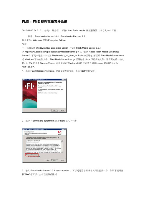
FMS + FME视频在线直播系统2010-11-17 04:21:31| 分类:服务器| 标签:fms flash media 视频服务器|字号大中小订阅软件:Flash Media Server 3.0.1 ;Flash Media Encoder 2.5服务平台:Windows 2003 Enterprise Edition安装:一、在服务器Windows 2003 Enterprise Edition上安装Flash Media Server 3.0.1从/products/flashmediastreaming/可以下载到Adobe Flash Media Streaming Server 3,下到本地是一个名为Flashmedia3_Int_Strm_ALP.zip的压缩包,解压后FlashMediaServer3.exe 是Windows下的安装文件,FlashMediaServer3.tar.gz压缩包是Linux下的安装文件,还有其它的一些文档,H.264的几个Sample Video。
在这里以在Windows 2003下安装为例,Windows 2003IP地址为192.168.1.7。
1、双击FlashMediaServer3.exe,出现安装开始界面, 点击“Next”开始安装2、选中“I accept the agreement”点击“Next”进入下一步3、输入Flash Media Server 3.0.1 serial number ,可以通过算号器或者从网上搜索一个,如果不填写直接“Next”也可以,会有连接数的限制4、准备好将要开始安装了5、设置好安装的路径,默认的安装路径是“C:\Program Files\Adobe\Flash Media Server 3\”,这里更改为“C:\FMS”,点击“Next”继续6、在开始程序菜单中将显示的名字,这里不做更改7、设置管理员的帐号和密码,安装好后可以使用这个帐号和密码进入管理界面8、设置端口号,可以同时设置多个,以逗号分隔,注意不要和现在服务使用的端口发生冲突。