EDA仿真软件介绍
射频EDA仿真软件介绍

射频EDA仿真软件介绍射频EDA(Electronic Design Automation)是一种用于射频芯片设计和仿真的软件工具,它通过电磁场仿真和电路仿真等功能,可以帮助设计者优化射频电路的性能和可靠性。
本文将介绍几款常用的射频EDA仿真软件。
1. ADS(Advanced Design System)ADS是美国Keysight(前身为安捷伦科技)推出的一款强大的射频和微波电路设计和仿真工具。
它包含了多种电路仿真方法,如基于S参数的线性仿真、基于混合EM的电磁仿真和基于直接时间域的高速数字仿真等。
ADS还内置了丰富的器件模型和库,方便用户进行仿真和优化。
此外,ADS还支持与SI/PI和系统仿真软件的集成,使得整个设计流程更加高效。
2. HFSS(High Frequency Structure Simulator)HFSS是美国ANSYS公司开发的一种基于有限元分析(FiniteElement Analysis)的高性能电磁场仿真软件。
它主要用于射频和微波领域,可以模拟复杂的电磁场分布和信号传输。
HFSS具有优异的求解速度和准确度,并且支持多种仿真技术,如频域仿真、时域仿真和混合仿真等。
此外,HFSS还提供了强大的后处理功能,可以用于绘制场强分布图、辐射图和散射参数图等。
3. CST Studio SuiteCST Studio Suite是德国CST公司开发的一款电磁场仿真软件套件,广泛应用于射频、天线和微波电路的设计和仿真。
CST基于有限差分时域(FDTD)方法,具有较高的计算速度和较低的内存占用。
CST StudioSuite提供了丰富的建模功能和后处理工具,可以实现多尺度建模、参数扫描和优化等操作。
此外,CST还支持与ADS和HFSS等软件的数据交换,方便不同工具之间的协同设计和分析。
4. AWR Microwave OfficeAWR Microwave Office是美国National Instruments(前身为奇美电子)开发的一款射频和微波电路设计软件。
EDA仿真软件介绍

EDA仿真软件介绍 (2009-03-21 08:41)分类:EDAEDA技术是在电子CAD技术基础上发展起来的计算机软件系统,是指以计算机为工作平台,融合了应用电子技术、计算机技术、信息处理及智能化技术的最新成果,进行电子产品的自动设计。
利用EDA工具,电子设计师可以从概念、算法、协议等开始设计电子系统,大量工作可以通过计算机完成,并可以将电子产品从电路设计、性能分析到设计出IC版图或PCB版图的整个过程的计算机上自动处理完成。
现在对EDA的概念或范畴用得很宽。
包括在机械、电子、通信、航空航天、化工、矿产、生物、医学、军事等各个领域,都有EDA的应用。
目前EDA技术已在各大公司、企事业单位和科研教学部门广泛使用。
例如在飞机制造过程中,从设计、性能测试及特性分析直到飞行模拟,都可能涉及到E DA技术。
本文所指的ED A技术,主要针对电子电路设计、PCB设计和I C设计。
EDA设计可分为系统级、电路级和物理实现级。
2 EDA常用软件EDA工具层出不穷,目前进入我国并具有广泛影响的EDA软件有:multiSI M7(原EWB的最新版本)、PSPICE、OrCAD、PCAD、Protel、Viewlog ic、Mentor、Graphic s、Synopsy s、LSIIogi c、Cadence、MicroSi m 等等。
这些工具都有较强的功能,一般可用于几个方面,例如很多软件都可以进行电路设计与仿真,同进还可以进行PCB自动布局布线,可输出多种网表文件与第三方软件接口。
(下面是关于ED A的软件介绍,有兴趣的话,旧看看吧^^^)下面按主要功能或主要应用场合,分为电路设计与仿真工具、PCB设计软件、IC 设计软件、PLD设计工具及其它EDA软件,进行简单介绍。
proteus软件简介

DS18B20温度传感器:
阻、电容、二极管、 晶体管、 SCRs、 光耦合器、 运放、 555 定时 器等;74 系列TTL 和 4000 系列 CMOS 器件; 存储器:ROM、 RAM、EEPROM、I2C 器件等;微控制器支持的器件如I/O 口、 USART 等;
-
➢ 快捷选取/放置器件:通过模糊搜索可快速从器件
库中选取器件。
-
(3)PROTEUS是单片机课程设计、毕业设 计的创作园地
课程设计、毕业设计是学生走向就业的 重要实践环节。由于PROTEUS提供了实验 室无法相比的大量的元器件库,提供了修改 电路设计的灵活性、提供了实验室在数量、 质量上难以相比的虚拟仪器、仪表,因而也 提供了培养学生实践精神、创造精神的平台 。
-
Proteus
ISIS 原理图设计系统
ARES PCB设计系统
-
1、ISIS(智能原理图输入系统)
ISIS是整个Proteus的中心部分,是一个强 大的原理图绘制系统。
➢ 个性化的编辑环境:用户可自定义图形外观,包括线宽、填充类型、
字符等,也可以使用模板。
➢ 丰富的元器件库:包含超过6000 种器件模型:标准电子元件:电
-
本系统需要用到的元器件
AT89C52
DS18B20
BUZZER(蜂鸣 器)
12864液晶
RESPACK(排阻)PNP(三极管)
BUTTON按键 LED
POT(滑动变阻 器)
-
快速旋转元器件:
如上图所示,当液晶数据端口要与单片机P2口相连时,显 然把液晶旋转90度比较好连,有一种方法是鼠标右键单击 器件可以旋转旋转,快速的方法是设置一个快捷键,菜单 栏System Set Keyboard Map Object Context Command选择自己喜欢的快捷键
常用EDA软件简介

常用EDA软件简介摘要:在电子通信领域中,着重对multisim,orcad-pspice,protel,proteus,keil与matlab六种eda软件进行了介绍,并对各软件所适用的场合进行了对比,得出了各自的优势,同时对eda 软件今后的应用与发展提出了预测,为电子领域的初学者提供了一定的指导与参考价值。
关键词:multisim;orcad-pspice;protel;proteus;keil;matlab中图分类号:tp319 文献标识码:a 文章编号:1007-9599 (2013) 03-0000-02eda技术是指以计算机为辅助工具,将电子、计算机、数据分析、图像处理等技术融为一体的具有智能化的电子辅助手段。
利用eda 软件工具,科研工作者可直接对设计思想进行验证,从而省去了大量的人力、物力和财力,避免了在实际设计中大量流程,提高了效率,缩短了电子产品的开发周期,并可方便快捷的对所设计的电路、算法等性能进行实时操作与优化。
在不同的工作领域中出现有大量的eda软件。
本文着重对电子通信领域中常见的几种eda软件进行对比,找出各软件在不同应用场合的优势。
1 常用eda软件在电子通信领域中,eda软件按用途分电路设计、功能仿真、版图绘制、软件编程等,其中常见的软件有multisim(原ewb)、orcad-pspice、protel、proteus、keil和matlab等。
一般每种软件都以一种或两种功能为主,并附带有其它功能。
下面对上述软件逐一介绍。
1.1 multisim软件multisim软件是加拿大ewb的前身,后并入美国国家仪器有限公司。
multisim主要利用了电路原理图、电路硬件描述语言针对模拟电路、数字电路、模数混合电路的设计与仿真,具有强大的仿真与分析能力。
multisim软件是一个专门用于电子电路设计与仿真的eda工具软件,具有直观的图形界面、丰富的元器件库、强大的仿真分析能力、丰富的虚拟测试仪器(如万用表、示波器、函数发生器、波特仪等),学习与应用相对较容易,很适合初学者对电子电路的学习。
EDA软件介绍
MAX+plus IIMax+plusⅡ是Altera公司上一代的PLD开发软件,提供的FPGA/CPLD开发集成环境,Altera是世界上最大可编程逻辑器件的供应商之一。
Max+plusⅡ界面友好,使用便捷,被誉为业界最易用易学的EDA软件。
在Max+plusⅡ上可以完成设计输入、元件适配、时序仿真和功能仿真、编程下载整个流程,它提供了一种与结构无关的设计环境,使设计者能方便地进行设计输入、快速处理和器件编程。
目前Altera已经停止开发MaxplusII,而转向QuartusII软件平台。
[1]Max+plusⅡ开发系统的特点1、开放的界面Max+plusⅡ支持与Cadence,Exemplarlogic,Mentor Graphics,Synplicty,Viewlogic和其它公司所提供的EDA工具接口。
2、与结构无关Max+plusⅡ系统的核心Complier支持Altera公司的FLEX10K、FLEX8000、FLEX6000、MAX9000、MAX7000、MAX5000和Classic可编程逻辑器件,提供了世界上唯一真正与结构无关的可编程逻辑设计环境。
3、完全集成化Max+plusⅡ的设计输入、处理与较验功能全部集成在统一的开发环境下,这样可以加快动态调试、缩短开发周期。
4、丰富的设计库Max+plusⅡ提供丰富的库单元供设计者调用,其中包括74系列的全部器件和多种特殊的逻辑功能(Macro-Function)以及新型的参数化的兆功能(Mage-Function)。
5、模块化工具设计人员可以从各种设计输入、处理和较验选项中进行选择从而使设计环境用户化。
6、硬件描述语言(HDL)Max+plusⅡ软件支持各种HDL设计输入选项,包括VHDL、Verilog HDL和Altera自己的硬件描述语言AHDL。
7、Opencore特征Max+plusⅡ软件具有开放核的特点,允许设计人员添加自己认为有价值的宏函数。
eda简介(eda简介)
---------------------------------------------------------------最新资料推荐------------------------------------------------------eda简介(eda简介)eda 简介(eda 简介) EDA in the communications industry (Telecommunication) another explanation is the enterprise data architecture, EDA gives a general view of an enterprise data architecture, and in accordance with the characteristics of telecom enterprises, the framework and hierarchy. EDA is an electronic design automation (Electronic Design Automation): from the computer aided design in the middle of 1960s (CAD), computer aided manufacturing (CAM), computer aided test (CAT) and Computer Aided Engineering (CAE) and the concept of development. Catalog First, what is EDA? Two, design methods Three 、 EDA tool software classification Four, EDA tool software vendors tycoon three Five, compounds Six. Exploratory data analysis Seven. Distribution estimation algorithm 1. What is EDA? Two, design methods Three 、 EDA tool software classification Four, EDA tool software vendors tycoon three Five, compounds Six. Exploratory data analysis Seven, distribution estimation algorithm Edit this paragraph 1. What is EDA? In 1990s, the international advanced electronic and computer technology in the world, has been exploring new methods of electronic circuit design actively,1 / 23and made a thorough change in design methods, tools etc, with great success. In the field of electronic technology design, the application of programmable logic devices (such as CPLD, FPGA) has been widely popularized. These devices bring great flexibility to the design of digital systems. These devices can be programmed by software to reconstruct their hardware structure and working mode, so that the hardware design can be as convenient and fast as the software design. All these greatly changed the traditional digital system design method, design process and design concept, and promoted the rapid development of EDA technology. EDA technology is a computer as a tool for designers in the EDA software platform, using hardware description language VHDL to complete the design documents, and then the computer automatically complete logic compilation, simplification, segmentation, synthesis, optimization, layout, simulation, adaptive translation, logical mapping and programming work until the chip for the specific target the. The emergence of EDA technology greatly improves the efficiency and operability of circuit design, and reduces the labor intensity of designers. Using EDA tools, the electronics designer can start the electronic system design from concept, algorithm and protocol, a lot of work can be done through the---------------------------------------------------------------最新资料推荐------------------------------------------------------ computer and electronic products can be from circuit design and performance analysis to design the whole process of IC territory or PCB layout of the computer automatically complete the processing. Now, the concept or category of EDA is very wide. Including mechanical, electronic, communications, aerospace, chemical, mineral, biological, medical, military and other fields, there are EDA applications. At present, EDA technology has been widely used in major companies, enterprises and institutions and scientific research and teaching departments. For example, in the aircraft manufacturing process, from design, performance testing and characteristic analysis until the flight simulation, may involve EDA technology. The concept of EDA EDA technology refers to the computer as the work platform, the latest achievements of the integration application of electronic technology, computer technology, information processing and intelligent technology, the automatic design of electronic products. Using EDA tools, the electronics designer can start the electronic system design from concept, algorithm and protocol, a lot of work can be done through the computer and electronic products can be from circuit design and performance analysis to design the whole process of IC3 / 23territory or PCB layout of the computer automatically complete the processing. Now, the concept or category of EDA is very wide. Including mechanical, electronic, communications, aerospace, chemical, mineral, biological, medical, military and other fields, there are EDA applications. At present, EDA technology has been widely used in major companies, enterprises and institutions and scientific research and teaching departments. For example, in the aircraft manufacturing process, from design, performance testing and characteristic analysis until the flight simulation, may involve EDA technology. This paper refers to the EDA technology, mainly for electronic circuit design, PCB design and IC design. EDA design can be divided into system level, circuit level and physical implementation level. Edit paragraph two, design method (1) front end design (system modeling, RTL level description), back end design (FPGAASIC) system modeling (2) IP multiplexing (3) front-end design (4) system description: establish the mathematical model of the system. (5) function description: describe the behavior of the system or the data flow diagram among the sub modules. (6) logic design: the system function is structured, usually with text, schematics, logic diagrams, Boolean expressions to represent the design results. (7)---------------------------------------------------------------最新资料推荐------------------------------------------------------ simulation: including function simulation and timing simulation, mainly verify the correctness and timing characteristics of the system function. Edit this paragraph three, EDA tool software classification EDA tool software can be roughly divided into three categories: chip design assistance software, programmable chip aided design software, system design auxiliary software and so on. Currently entering the country and has a wide influence in the EDA software system design software and programmable chip design software: Protel, Altium Designer, PSPICE, multiSIM10 (the latest version of the original EWB, OrCAD, PCAD), LSIIogic, MicroSim, ISE, Modelsim, Matlab and so on. These tools are strong function, generally can be used in several aspects such as many software can realize the circuit design and simulation, PCB automatic layout and also can output a variety of file with third party software interface. According to the main function or the main application situation, divided into circuit design and simulation tools, PCB design software, IC design software, PLD design tools and other EDA software, a brief introduction. 3.1 electronic circuit design and simulation tools, we may have used the test board or something else to make some electronic5 / 23system to practice. But sometimes, we find that there are a lot of problems to be done, not previously thought, so that waste our time and supplies. It also increases the product development cycle and extends the product listing time, so that the product loses the market competitive advantage. Is there a way to know the result without using the electric iron test board? The conclusion is that this is the circuit design and simulation technology. When it comes to electronic circuit design and simulation tools, this technology can not be mentioned in the United States, can not help but mention their aircraft design why high efficiency. Our previous design of a medium-sized aircraft, from the draft to the detailed design to the wind tunnel test, and finally to the map to the actual production, the entire cycle is about 10 years. And the United States is 1 years old. Why is there such a big gap? Because the United States is most used in the design of virtual simulation technology, the wind tunnel experiment parameters accumulated over the years into the computer, and then through the computer programming written in a virtual environment of software, and enable it to experience parameters automatically apply the relevant formula and call after long-term accumulated input computer. In this way, as long as the aircraft shape meter data---------------------------------------------------------------最新资料推荐------------------------------------------------------in the virtual wind tunnel test software, where unreasonable have changes there, until the best effect, efficiency is high, as long as the final test several times for shortage in the actual environment can be established, from their Boeing 747 to F16 is this method uses the. The aerodynamic data are provided by senior experts, and the software developer is IBM. The engineer of the aerocraft only needs to use the simulation software to do a variety of simulation debugging work on the computer platform. Similarly, many of their other things are using a similar approach, from big to small, from complexity to simplicity, and even to design furniture and composition, but the specific content of the software is different. In fact, they invented the first generation of computers for this purpose (originally for efficient design of artillery and related shells and other large amount of design). Electronic circuit design and simulation tools include SPICE/PSPICE; multiSIM7; Matlab; SystemView; mmicad LiveWire、爱迪生、蒂娜亲明亮的火花等。
最常用的几种EDA软件

最常用的几种EDA软件EDA技术是在电子CAD技术基础上发展起来的计算机软件系统,是指以计算机为工作平台,融合了应用电子技术、计算机技术、信息处理及智能化技术的最新成果,进行电子产品的自动设计。
利用EDA工具,电子设计师可以从概念、算法、协议等开始设计电子系统,大量工作可以通过计算机完成,并可以将电子产品从电路设计、性能分析到设计出IC版图或PCB版图的整个过程在计算机上自动处理完成。
现在对EDA的概念或范畴用得很宽。
包括在机械、电子、通信、航空航天、化工、矿产、生物、医学、军事等各个领域,都有EDA的应用。
目前EDA 技术已在各大公司、企事业单位和科研教学部门广泛使用。
例如在飞机制造过程中,从设计、性能测试及特性分析直到飞行模拟,都可能涉及到EDA技术。
本文所指的EDA技术,主要针对电子电路设计、PCB设计和IC设计。
EDA 设计可分为系统级、电路级和物理实现级。
EDA常用软件EDA工具层出不穷,目前进入我国并具有广泛影响的EDA软件有:EWB、PSPICE、OrCAD、PCAD、Protel、ViewLogic、Mentor、Graphics、Synopsys、LSIlogic、Cadence、MicroSim等等。
这些工具都有较强的功能,一般可用于几个方面,例如很多软件都可以进行电路设计与仿真,同时以可以进行PCB自动布局布线,可输出多种网表文件与第三方软件接口。
下面按主要功能或主要应用场合,分为电路设计与仿真工具、PCB设计软件、IC 设计软件、PLD设计工具及其它EDA软件,进行简单介绍。
1、电子电路设计与仿真工具电子电路设计与仿真工具包括SPICE/PSPICE;EWB;Matlab;SystemView;MMICAD 等。
下面简单介绍前三个软件。
(1)SPICE(Simulation Program with Integrated Circuit Emphasis)是由美国加州大学推出的电路分析仿真软件,是20世纪80年代世界上应用最广的电路设计软件,1998年被定为美国国家标准。
三款EDA工具,AD、PADS与Allegro的简单介绍
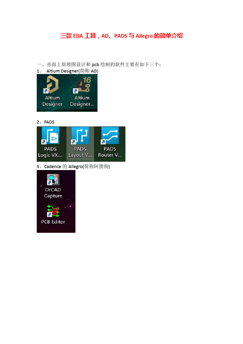
三款EDA工具,AD、PADS与Allegro的简单介绍一、市面上原理图设计和pcb绘制的软件主要有如下三个:1、Altium Designer(简称AD)2、PADS3、Cadence的Allegro(简称阿狸狗)二、三款软件的简单介绍Altium Designer:优点:1、软件界面友好,操作简单,适合入门,由于前身是protel99SE,有广大的学生会使用,有很好的群众基础。
2、绘制原理图和PCB都是在同一个软件。
缺点:1、非常吃电脑内存,一般的电脑用起来非常慢,需要配置比较高的电脑。
2、AD的容错率较差,如果粗心一点那么很可能导致出错。
3、大型公司使用AD比较少,工作上升空间不大。
应用场景:主要是一些简单的双层及四层板,市面上小型产品使用较多。
PADS:特点:有三个界面:PADS Logic 、PADS Layout 、PADS RouterPADS Logic用于原理图设计PADS Layout用于布局PADS Router用于布线应用场景:PADS目前主要流行在沿海地区,比如说广州、深圳。
PADS主要用在消费类电子产品,早期的VCD,DVD,MP3 ,MP4,U盘,液晶电视,到现在的平板电脑,行车记录仪,车载电子产品,导航仪,数字机顶盒,安卓智能电视盒、手机等都是由PADS绘制的。
PADS界面比较简单,上手还是比较容易的。
而且PAD画一下比较大型的板子比较好,在一些沿海发达地区找工作还是较为容易,薪资上升空间也不错。
Allegro:Allegro应该叫Cadence allegro。
Cadence是公司名,allegro是该公司旗下的设计软件,一般用OrCAD Capture画原理图,用Allegro画PCB。
优点:功能强大。
缺点:不好学,不容易上手。
应用:allegro一般只有大公司用,特别是做电脑主板的公司用,因为这个软件功能强大,画大型板子有优势。
如电脑主板,大型工控板,服务器主板,等大型板子,他的效率和优势非常明显。
- 1、下载文档前请自行甄别文档内容的完整性,平台不提供额外的编辑、内容补充、找答案等附加服务。
- 2、"仅部分预览"的文档,不可在线预览部分如存在完整性等问题,可反馈申请退款(可完整预览的文档不适用该条件!)。
- 3、如文档侵犯您的权益,请联系客服反馈,我们会尽快为您处理(人工客服工作时间:9:00-18:30)。
EDA仿真软件介绍
EDA(Electronic Design Automation)是一类电子设计自动化软件,用于辅助电子产品的设计与仿真。
EDA软件帮助工程师在电子产品的设计
过程中快速、准确地完成各种任务,从而提高设计效率和产品质量。
本文
将介绍几款常见的EDA仿真软件,以及它们的特点和优势。
1. Cadence Allegro
Cadence Allegro是一款功能强大的EDA仿真软件。
它提供了完整的
设计流程,包括原理图设计、PCB(Printed Circuit Board)布局和仿真。
Cadence Allegro可以帮助工程师快速设计复杂的电子电路,并进行各种
信号和功耗仿真。
该软件具有直观的用户界面,易于学习和使用。
此外,Cadence Allegro还提供了丰富的库和模型,方便用户进行各种电路设计
和仿真。
2. Mentor Graphics PADS
Mentor Graphics PADS是一款流行的EDA仿真软件,专门用于PCB
设计和仿真。
它提供了直观的用户界面,支持多种设计工具和功能,如原
理图设计、电路仿真、PCB布局和封装设计等。
此外,Mentor Graphics PADS还提供了强大的仿真和验证功能,可以帮助工程师检测电路的性能
和可靠性问题,提高产品的质量。
3. Altium Designer
Altium Designer是一款专业的PCB设计和仿真软件。
它提供了完整
的设计流程,包括原理图设计、PCB布局和仿真。
Altium Designer具有
友好的用户界面,支持多种设计工具和功能,如自动布线、3D模拟和原
理图捕捉等。
此外,Altium Designer还提供了丰富的库和模型,方便用
户进行各种电路设计和仿真。
4. Ansys HFSS
Ansys HFSS是一款强大的高频电磁场仿真软件。
它可以帮助工程师
对射频(Radio Frequency)和微波(Microwave)电路进行仿真,包括天
线设计、滤波器设计和射频电路设计等。
Ansys HFSS具有丰富的模型库
和仿真功能,可以快速预测电路的性能,并进行优化和验证。
5. Mentor Graphics HyperLynx
Mentor Graphics HyperLynx是一款专业的信号和功耗仿真软件。
它
可以帮助工程师评估电路的信号完整性和功耗特性,并提供优化建议。
HyperLynx具有直观的用户界面,支持多种仿真和分析工具,如信号完整
性仿真、电磁兼容性分析和电源完整性仿真等。
其高度集成的设计环境可
以提高设计效率和准确性。
总结起来,EDA仿真软件在电子产品设计中起到了至关重要的作用。
它们帮助工程师快速设计和仿真各种电子电路,提高设计效率和产品质量。
从常见的几款软件中可以看出,EDA仿真软件在功能、用户界面和模型库
方面都有其独特的特点和优势。
工程师可以根据自己的需求选择合适的软件,以提高设计效率和成果。