Magnon and Hole Excitations in the Two-Dimensional Half-filled Hubbard Model
PZT的半导体特性
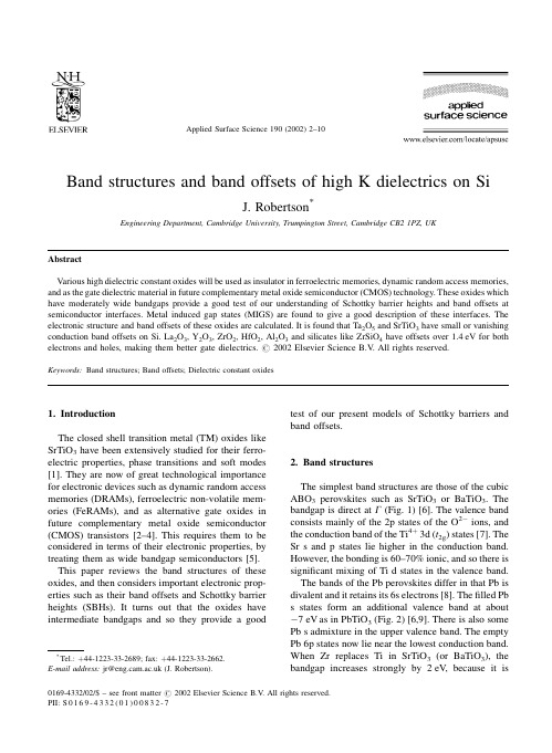
Band structures and band offsets of high K dielectrics on SiJ.Robertson *Engineering Department,Cambridge University,Trumpington Street,Cambridge CB21PZ,UKAbstractVarious high dielectric constant oxides will be used as insulator in ferroelectric memories,dynamic random access memories,and as the gate dielectric material in future complementary metal oxide semiconductor (CMOS)technology.These oxides which have moderately wide bandgaps provide a good test of our understanding of Schottky barrier heights and band offsets at semiconductor interfaces.Metal induced gap states (MIGS)are found to give a good description of these interfaces.The electronic structure and band offsets of these oxides are calculated.It is found that Ta 2O 5and SrTiO 3have small or vanishing conduction band offsets on 2O 3,Y 2O 3,ZrO 2,HfO 2,Al 2O 3and silicates like ZrSiO 4have offsets over 1.4eV for both electrons and holes,making them better gate dielectrics.#2002Elsevier Science B.V .All rights reserved.Keywords:Band structures;Band offsets;Dielectric constant oxides1.IntroductionThe closed shell transition metal (TM)oxides like SrTiO 3have been extensively studied for their ferro-electric properties,phase transitions and soft modes [1].They are now of great technological importance for electronic devices such as dynamic random access memories (DRAMs),ferroelectric non-volatile mem-ories (FeRAMs),and as alternative gate oxides in future complementary metal oxide semiconductor (CMOS)transistors [2±4].This requires them to be considered in terms of their electronic properties,by treating them as wide bandgap semiconductors [5].This paper reviews the band structures of these oxides,and then considers important electronic prop-erties such as their band offsets and Schottky barrier heights (SBHs).It turns out that the oxides have intermediate bandgaps and so they provide a goodtest of our present models of Schottky barriers and band offsets.2.Band structuresThe simplest band structures are those of the cubic ABO 3perovskites such as SrTiO 3or BaTiO 3.The bandgap is direct at G (Fig.1)[6].The valence band consists mainly of the 2p states of the O 2Àions,and the conduction band of the Ti 4 3d (t 2g )states [7].The Sr s and p states lie higher in the conduction band.However,the bonding is 60±70%ionic,and so there is signi®cant mixing of Ti d states in the valence band.The bands of the Pb perovskites differ in that Pb is divalent and it retains its 6s electrons [8].The ®lled Pb s states form an additional valence band at about À7eV as in PbTiO 3(Fig.2)[6,9].There is also some Pb s admixture in the upper valence band.The empty Pb 6p states now lie near the lowest conduction band.When Zr replaces Ti in SrTiO 3(or BaTiO 3),the bandgap increases strongly by 2eV,because itisApplied Surface Science 190(2002)2±10*Tel.: 44-1223-33-2689;fax: 44-1223-33-2662.E-mail address:jr@ (J.Robertson).0169-4332/02/$±see front matter #2002Elsevier Science B.V .All rights reserved.PII:S 0169-4332(01)00832-7controlled by the energy of the Zr d states.In contrast,in PZT,the Pb 6p states form the conduction band minimum,so the gap barely increases from 3.3to 3.7eV [10].It is recognised that the resonant covalence of Ti-d/O-p states is the origin of ferroelectricity in SrTiO 3type perovskites [11].In Pb perovskites,there is additional resonant covalence between Pb s and O p states which increases the ferroelectric polarity.SrBi 2Ta 2O 9is a layered crystal built from perovs-kite blocks separated by Bi 2O 2layers.It turns out that the Bi s and p states form the highest valence band and lowest conduction bands,respectively,while the ferro-electric response originates mainly from the TaO 3perovskite blocks [12].There is therefore an interest-ing separation of the functionality onto the Ta and Bi sub-lattices.Cubic ZrO 2has the ¯uorite structure.It has a simple band structure,as shown in Fig.3.The O p states form the valence band with a maximum at X [13].The conduction band minimum is at G ,and consists of Zr d states.The Zr d x 2Ày 2and d z 2states lie below the d xy states.The Zr s state lies midway between these at G ,but it disperses rapidly upwards.2.1.Models of Schottky barriers and semiconductor heterojunctionsThe band line-up of two semiconductors is deter-mined,like the SBH of a semiconductor on a metal,by charge transfer across the interface and the presence of any dipole layer at the interface.The charge transfer is that between the metal and the interface states of the semiconductor (Fig.4)[14].The charge transfertendsFig.1.Band structure of BaTiO 3calculated by pseudo-potential method [6].J.Robertson /Applied Surface Science 190(2002)2±103to align the Fermi level E F of the metal to the energy level of the interface states.The SBH for electrons f n between a semiconductor S and a metal M is f n S F M ÀF S F S Àw S(1)Here,F M is the work function of the metal,F S the energy of the semiconductor interface states,w S the semiconductor's electron af®nity (EA)and S the Schottky pinning parameter.S is given by [15]S11 e 2N d =ee 0(2)where e is the electronic charge,e 0the permittivity of free space,N the areal density of the interface states and d their decay length in the semiconductor.The dimensionless pinning factor S describes if the barrieris `pinned'or not.S varies between the limits S 1for unpinned Schottky barriers,and S 0for `Bardeen'barriers pinned by a high density of interface states in which the SBH is f n F S Àw S .There are numerous models of the origins of inter-face states,both intrinsic and extrinsic.In the intrinsic model originating from Bardeen and Heine,a semi-in®nite semiconductor in contact with a metal pos-sesses intrinsic states which are now called metal-induced gap states (MIGS)by Tersoff [14].F S is then the charge neutrality level (CNL)of the interface states,de®ned as the energy above which the states are empty for a neutral surface [16±18].On the other hand,the extrinsic models stress that the metal can react with the semiconductor [19].Brillson correlated the heat of reaction with S .This reaction maycreateFig.2.Band structure of PbTiO 3calculated by pseudo-potential method [6].4J.Robertson /Applied Surface Science 190(2002)2±10interface defects such as vacancies,whose gap states can pin the metal Fermi level,as noted by Spicer [20]and Dow [21].These models were supported by theobservation that pinning occurs even for monolayer coverage of metal,before the MIGS could be estab-lished.It is now believed that,overall,the intrinsic model gives a better description of Schottky barriers,because intrinsic states have a larger pinning dipole,N d ,than surface defects.The pinning parameter S has been in¯uential in our empirical understanding of Schottky barriers.Some years ago,Kurtin et al.[22]noted that S seemed to vary sharply with the ionicity of semi-conductor (Fig.5),from near 0for low ionicity semiconductors like Si and GaAs to 1for higher ionicity solids like SiO 2,SrTiO 3and KTaO 3.S is a dimensionless slope of barrier height to metal work function,S@f n @F M(3)Fig.3.Band structure of ZrO 2calculated by pseudo-potential method[6].Fig.4.Schematic diagram of SBHs.J.Robertson /Applied Surface Science 190(2002)2±105However,Louie [23]and Schluter [24]noted that Kurtin [22]had actually correlated the barrier heights to S H :S H@f n @X(4)which is the slope of barrier height to the Pauling electronegativity of the metal,and not the dimension-less S in (4).The work function and electronegativity vary roughly as [25,26]:F M 2:27X M 0:34(5)Thus,S H 2:27S ,and the Schottky limit should be S H 2:27.The data rarely reach this limit and Schluter [24]observed that S had a better correlation with the dielectric constant of the semiconductor e 0.Empiri-cally,Mo Ènch [14,27]found that S varied with e I as S11 0:1 e I À1 2(6)Certain materials are key tests of Schottky barriermodels.Diamond and xenon [14,28]have zero ioni-city but small e I ,and so their large S values show that S depends on e not on ionicity.This is tested by plotting log 1= S À1 against log e I À1 as in Fig.6.The wide gap oxides provide another key test,because they have intermediate e I values.SrTiO 3and KTaO 3were taken as high ionicity solids in the original Kurtin plot,with S H $1.However,this wasbefore data was actually known.When data [29]became available for SrTiO 3,showing S lying between 0.25and 0.4(Fig.6),it was clear that S is much lower.SrTiO 3falls well on the trend in Fig.3.The reason for this is that the SBHs depend on e I .e I is controlled by the states closest to the bandgap [5].In SrTiO 3,these are the moderately ionic Ti±O states of Ti±O bonds,not the highly ionic Sr±O states which lie well away from the gap and provide a much smaller contribution to e I .This can be seen in the partial density of states (DOS)of SrTiO 3in Fig.6.Thus,SrTiO 3and KTaO 3were misplaced in Fig.5as highly ionic solids.A lesser point is that the moderate value of S of SrTiO 3clearly correlates with e I ,and not with the low frequency dielectric constant e 0,which has a very large value for ferroelectrics and would give S %0from (6).SrTiO 3also serves as an evidence against the defect model,in that the barrier lies some way into the gap,not at the conduction band edge where the O vacancy states lie and would cause pinning.In sum-mary,the MIGS model of Schottky barriers holds for a wide range of solids of various ionicity and dielectric constants [5].The band alignment between two semiconductors is controlled by charge transfer and interface dipoles,just as Schottky barriers [30].For no dipoles,the Schottky limit,the conduction band offset isgivenFig.5.Schottky barrier pinning factor S H in the (incorrect)model of Kurtin etal.Fig. 6.Log±log plot of 1= S À1 vs.e I À1for various semiconductors and insulators to verify the MIGS model of Schottky barrier pinning factor S .6J.Robertson /Applied Surface Science 190(2002)2±10by the difference in their electron af®nities,the `elec-tron af®nity rule'.A similar idea was that for no charge transfer,the band line-ups are derived by placing each semiconductor's band on an absolute energy scale such as those of the free atom energy levels [31].Tersoff [16]showed that the band offset between two semiconductors a and b is controlled by interface dipoles as in the Schottky barrier,and so the conduc-tion band offset is given by f n w a ÀF CNL ;a À w b ÀF CNL ;bS F CNL ;a ÀF CNL ;b(7)The offsets are now described by aligning the CNLs of each semiconductor,modi®ed by the S factor.For simple semiconductors like Si,e I is large,and so S is small and the third term was negligible in the original formulation,but it is retained here for wide gap oxides.For strong pinning,the alignment is just given by the alignment of the two CNLs.The CNL energy below the vacuum level is a measure of the mean electronegativity of the semiconductor,in the same way that the work function of a metal is propor-tional to the metal's electronegativity.Thus,Eq.(7)says that the band alignment is the difference in electronegativity screened by the S factor.A wide ranging quantitative comparison found that the CNL models gives a good description of the band offsets [30].The CNL is the branch point of the semiconductor interface states.It is the integral of the Green's func-tion of the band structure,taken over the Brillouin zone [17],G E ZBZ N E H d H EE ÀE H0(8)Cardona and Christensen later provided a quicker method using a sum over special points of the Bril-louin zone [5,32].G E X i 1E ÀE i (9)2.2.Application to oxidesThe band alignments for the various wide gapoxides in contact with metal or silicon are found by calculating their CNLs and S parameters.The S factors are found from (6)using the experimental values of e Iand are shown in Table 1.The CNLs were found by calculating the oxide band structures by the tight-binding method [5,6,8,33].The tight-binding para-meters are found by ®tting to existing band structures [9,10,34],photoemission spectra and optical data [2,35±37].The CNLs for the various oxides are given in Table 1,together with the experimental values of their bandgaps and electron af®nities [2,38].SrTiO 3is an important oxide for future DRAM capacitor dielectrics.SrTiO 3is also the most studied system and the best test of our calculations.Fig.7compares the predicted SBHs of SrTiO 3on various metals with the experimental values [30,39±43].The experimental data are quite scattered but are quite consistent with S !1and our calculated value of 0.28.This shows that SrTiO 3is a key oxide in the tests of Schottky barrier models.The calculated barrier height for SrTiO 3on Pt is 0.9eV ,which is close to the 0.8eV found by photoemission by Copel et al.[43].However we cannot account for the much larger S value found by Shimizu et al.[42].BaTiO 3has similar band offsets to SrTiO 3.PbTi x Zr 1Àx O 3or PZT is an important ferroelectric for non-volatile memories,optical memories and other applications.The predicted barrier height for Pt onTable 1Calculated values for various oxides of their CNL and conduction band (CB)offset with Si aGap (eV)EA (eV)CNL (eV)e I S CB offset (eV)SiO 290.9 2.250.86 3.5b Si 3N 4 5.3 2.1 4.10.51 2.4b Ta 2O 5 4.4 3.3 3.3 4.840.40.3BaTiO 3 3.3 3.9 2.6 6.10.28À0.1BaZrO 3 5.3 2.6 3.740.530.8TiO 2 3.05 3.9 2.27.80.180.05ZrO 2 5.8 2.5 3.6 4.80.41 1.4HfO 26 2.5 3.740.53 1.5Al 2O 38.81c 5.5 3.40.63 2.8Y 2O 362c 2.4 4.40.46 2.3La 2O 36c 2c 2.440.53 2.3ZrSiO 46.5 2.4 3.6 3.80.56 1.5SrBi 2Ta 2O 94.13.53.35.30.4aExperimental values [36,37]of the bandgap,EA [2,38],dielectric constant e I [37]are also given.In Eqs.(2)and (5),F S is the energy of the CNL below the vacuum level,in this table,it is its energy above the valence band.bExperimental values.cEstimated values.J.Robertson /Applied Surface Science 190(2002)2±107PZT (Pb 0.55Zr 0.45O 3)is 1.45eV ,which is close to the 1.5eV measured by Dey et al.[44].The electron barrier of Pt on PZT is larger than that on BST because its CNL lies lower in the gap.This is because of the different band structure of PZT,in which the Pb 6s and 6p states form the band edges and this tends to lower the CNL.The larger value of the hole barrier than the electron barrier means that PZT thin ®lms can have predominantly electron injection,even though bulk PZT tends to be p-type.SrBi 2Ta 2O 9(SBT)is an important ferroelectric for non-volatile memories [2,45].It does not suffer from the loss of switchable polarisation (fatigue)when used with Pt electrodes,which is a problem for PZT.Note that more recent optical data ®nd that the bandgap of SBT is 4.1eV [2].The Schottky barrier of Pt is predicted to be 1.2eV ,which is essentially the same as that found by photoemission [46].There is an important need for high dielectric constant oxides to act as gate oxides instead of silicon dioxide [3,4].This is because the SiO 2layer is now so thin (2nm),that it no longer acts as a good insulator because of direct tunnelling across it.The solution is to replace SiO 2with a thicker layer of a medium k oxide,with the same equivalent capacitance or `equivalence oxide thickness't ox .The oxides must also satisfy certain other conditions,including chemi-cal stability in contact with Si [47].This rules out Ti and Ta which both react with Si to form SiO 2.The other key requirement is that they act as barriers toboth electrons and holes [5,32].This requires that both their valence and conduction band offsets be over 1eV .There is presently considerable effort to identify the most effective oxide,from a choice of ZrO 2,HfO 2,La 2O 3,Y 2O 3,Al 2O 3and the silicates ZrSiO 4and HfSiO 4.The calculated CB band offsets with Si are given in Table 1and summarised in Fig.8.They are compared in Table 2with recent experimental values [48±53],which is seen to be in good agreement.The important feature of Ta 2O 5and SrTiO 3is that both of them have CB offsets on Si under 1eV ,in fact 0in the case of SrTiO 3.This prediction was recently con®rmed by photoemission data of Chambers et al.[48].This means that SrTiO 3or BST cannot be a good gate oxide.The calculated CB offset for Ta 2O 5is only 0.36eV for Ta 2O 5on Si.This is consistent with recent photoemission data of Miyazaki and Hirose [49].Data for Ta 2O 5gate FETS also showed only a small elec-tron barrier [50].The CB offsets for BST and Ta 2O 5and BST are small or negligible because the bandgap is quite small and the band offsets are so asymmetric.To increasetheparison of calculated and observed SBHs of SrTiO 3on variousmetals.Fig.8.Predicted band offsets of various oxides on Si.Table 2Comparison of calculated and experimental values [48±53]of conduction band offsets on SiCalculatedExperiment References Ta 2O 50.350Miyazaki SrTiO 3À0.1<0.1Chambers ZrO 2 1.4 1.4Miyazaki 2.0Houssa Al 2O 32.82.8Ludeke8J.Robertson /Applied Surface Science 190(2002)2±10CB offset,we must either increase the bandgap or lower the CNL.The gap can be increased by raising the TM d levels,by using4d or5d metals instead of3d metals or using group IIIB metals instead of group IV. We should use zirconates,not titanates.The gap of BaZrO3is2eV wider than BaTiO3.Its offset is0.8eV.A better strategy is to lower the CNL.The CNL is lowered if the metal valence is lowered from4to3. Indeed,in Y2O3and La2O3,the CNL is much lower in the bandgap.Y2O3and La2O3are the oxides with largest CB offsets for reasonable dielectric constants. ZrO2has a bandgap of5.8eV,which is slightly wider than BaZrO3,and it also has a lower metal/ oxygen stoichiometry.This gives a larger CB offset for ZrO2(1.4eV)than BaZrO3,and indeed one which is just high enough.HfO2is similar.The calculated CB offset of1.4eV for ZrO2compares with an experi-mental value of1.4eV from photoemission[51]and a value of2eV by internal photoemission[52].This CB offset is large enough for devices.Zirconium silicate ZrSiO4and hafnium silicate HfSiO4are glassy oxides with bandgaps of $6.5eV.ZrSiO4consists of chains of alternate edge-sharing ZrO4and SiO2tetrahedra,with addi-tional Zr±O bonds between the chains,leading to an overall six-fold Zr coordination.We estimate the bandgap of ZrSiO4to be6.5eV.The calculated CB offsets are1.5eV,slightly more than ZrO2.Al2O3has a bandgap of8eV close to SiO2but with a higher k($9).Its calculated CB offset is2.8eV, which compares exactly with that measured by Ludeke et al.[53].Overall,the agreement between the calculated and subsequent experimental values for CB offsets in Table2is surprisingly good.References[1]M.E.Lines,X.Glass,Ferroelectrics,Oxford UniversityPress,Oxford,1990.[2]J.F.Scott,Ferroelectrics Rev.1(1998)1.[3]G.D.Wilk,R.M.Wallace,J.M.Anthony,J.Appl.Phys.89(2001)5243.[4]A.I.Kingon,J.P.Maria,S.K.Streiffer,Nature406(2000)1032.[5]J.Robertson,J.Vac.Sci.Technol.B18(2000)1785.[6]P.W.Peacock,J.Robertson,Unpublished work.[7]L.F.Mattheis,Phys.Rev.B6(1972)4718.[8]J.Robertson,W.L.Warren,B.A.Tuttle,D.Dimos,D.M.Smyth,Appl.Phys.Lett.63(1993)1519.[9]R.D.King-Smith,D.Vanderbilt,Phys.Rev.B49(1994)5828.[10]J.Robertson,W.L.Warren,B.A.Tuttle,J.Appl.Phys.77(1995)3975.[11]R.E.Cohen,Nature358(1992)136.[12]J.Robertson,C.W.Chen,W.L.Warren,C.D.Gutleben,Appl.Phys.Lett.69(1996)1704.[13]R.H.French,S.J.Glass,F.S.Ohuchi,Y.N.Xu,W.Y.Ching,Phys.Rev.B49(1994)5133.[14]W.MoÈnch,Phys.Rev.Lett.58(1987)1260.[15]W.MoÈnch,Surf.Sci.300(1994)928.[16]A.W.Cowley,S.M.Sze,J.Appl.Phys.36(1965)3212.[17]C.Tejedor,F.Flores,E.Louis,J.Phys.C10(1977)2163.[18]J.Tersoff,Phys.Rev.Lett.52(1984)465.[19]J.Tersoff,Phys.Rev.B30(1984)4874;J.Tersoff,Phys.Rev.B32(1985)6989.[20]L.J.Brillson,Surf.Sci.300(1994)909.[21]W.E.Spicer,T.Kendelewicz,N.Newman,K.K.Chin,I.Lindau,Surf.Sci.168(1986)240.[22]R.E.Allen,O.F.Sankey,J.D.Dow,Surf.Sci.168(1986)376.[23]S.Kurtin,T.C.McGill,C.A.Mead,Phys.Rev.Lett.30(1969)1433.[24]S.G.Louie,J.R.Chelikowsky,M.L.Cohen,Phys.Rev.B15(1977)2154.[25]M.Schluter,Phys.Rev.B17(1978)5044;M.Schluter,Thin Solid Films93(1982)3.[26]W.Gordy,W.J.O.Thomas,Phys.Rev.24(1956)439.[27]H.B.Michaelson,J.Appl.Phys.48(1977)4729.[28]W.MoÈnch,Phys.Rev.Lett.58(1986)1260.[29]W.MoÈnch,Europhys.Lett.27(1994)479.[30]R.C.Neville,C.A.Mead,J.Appl.Phys.43(1972)4657.[31]W.A.Harrison,J.Vac.Sci.Technol.14(1977)1016.[32]M.Cardona,N.E.Christensen,Phys.Rev.B35(1987)6182.[33]E.T.Yu,J.O.McCaldin,T.C.McGill,Solid State Phys.46(1992)1.[34]J.Robertson,C.W.Chen,Appl.Phys.Lett.74(1999)1168.[35]G.M.Rignanese,X.Gonze,A.Pasquarello,Phys.Rev.B63(2001)104305.[36]R.H.French,J.Am.Ceram.Soc.73(1990)477.[37]E.D.Palik,Handbook of Optical Properties of Solids,V ol.1±3,Academic Press,New York,1985.[38]W.Schmickler,J.W.Schultze,in:J.M.O'Bockris(Ed.),Modern Aspects of Electrochemistry,V ol.17,Plenum Press, London,1986.[39]G.W.Dietz,W.Antpohler,M.Klee,R.Waser,J.Appl.Phys.78(1995)6113.[40]H.Hasegawa,T.Nishino,J.Appl.Phys.69(1991)1501.[41]K.Abe,S.Komatsu,Jpn.J.Appl.Phys.31(1992)2985.[42]T.Shimizu,N.Gotoh,N.Shinozaki,H.Okushi,App.Surf.Sci.117(1997)400;()T.Shimizu,N.Gotoh,N.Shinozaki,H.Okushi,Mat.Res.Soc.Symp.Proc.(2000).[43]M.Copel,P.R.Duncombe,D.A.Neumayer,T.M.Shaw,R.M.Tromp,Appl.Phys.Lett.70(1997)3227.[44]S.K.Dey,J.J.Lee,P.Alluri,Jpn.J.Appl.Phys.34(1995)3134.[45]C.A.Paz de Araujo,J.D.Cuchiaro,L.D.McMillan,M.C.Scott,J.F.Scott,Nature374(1995)627.[46]C.D.Gutleben,Appl.Phys.Lett.71(1997)3444.[47]H.J.Hubbard,D.G.Schlom,J.Mater.Res.11(1996)2757.J.Robertson/Applied Surface Science190(2002)2±109[48]S.A.Chambers,Y.Liang,Z.Yu,R.Dropad,J.Ramdani,K.Eisenbeiser,Appl.Phys.Lett.77(2000)1662.[49]S.Miyazaki,Appl.Surface Science(2002)``these proceed-ings''.[50]S.Miyazaki,M.Narasaki,M.Ogasawara,M.Hirose,Microelec.Eng.59(2001)373.[51]A.Chatterjee,et al.,IEDM Tech Digest,1998,p.777.[52]M.Houssa,M.Tuominen,M.Nailli,V.Afansev, A.Stesmans,J.Appl.Phys.87(2000)8615.[53]R.Ludeke,M.T.Cuberes,E.Cartier,Appl.Phys.Lett.76(2000)2886;D.J.Maria,J.Appl.Phys.45(1974)5454.10J.Robertson/Applied Surface Science190(2002)2±10。
21925065_榴辉岩中单斜辉石-石榴子石镁同位素地质温度计评述

1000 0569/2020/036(06) 1705 18ActaPetrologicaSinica 岩石学报doi:10 18654/1000 0569/2020 06 04榴辉岩中单斜辉石 石榴子石镁同位素地质温度计评述黄宏炜1 杜瑾雪1 柯珊2HUANGHongWei1,DUJinXue1 andKEShan21 中国地质大学地球科学与资源学院,北京 1000832 中国地质大学地质过程与矿产资源国家重点实验室,北京 1000831 SchoolofEarthSciencesandResources,ChinaUniversityofGeosciences,Beijing100083,China2 StateKeyLaboratoryofGeologicalProcessesandMineralResources,ChinaUniversityofGeosciences,Beijing100083,China2019 11 14收稿,2020 04 08改回HuangHW,DuJXandKeS 2020 Reviewontheclinopyroxene garnetmagnesiumisotopegeothermometersforeclogites ActaPetrologicaSinica,36(6):1705-1718,doi:10 18654/1000 0569/2020 06 04Abstract Theremarkableequilibriummagnesiumisotopefractionationbetweenclinopyroxeneandgarnetobservedineclogitesmakesitapotentialhigh precisiongeothermometer Therefore,thispaperselects64pairsofclinopyroxene garnetmagnesiumisotopedataofeclogitesintheChinesesouthwesternTianshanorogen,intheDabie SuluorogenandintheKaapvaalcratonintheSouthAfricafromliteratures Then,wescreened50pairsofdatathatreachtheequilibriummagnesiumisotopefractionationbytheδ26MgCpx δ26MgGrtdiagram Usingthesemagnesiumisotopeequilibriumfractionationdata,wecalculatedpeaktemperaturesofeclogitesbymagnesiumisotopegeothermometersofHuangetal (2013)throughfirst principlescalculationandWangetal (2012)andLietal (2016)throughempiricalestimation,andcomparedthemwiththepeaktemperaturesgivenbyothergeothermometers Byanalyzingthecalculationresults,itisfoundthatfororogeniceclogites,thecalculationresultsofthegeothermometerofHuangetal (2013)areconsistentwiththosepreviouslyobtainedbytraditionalgeothermometersandphaseequilibriamodeling,whilethecalculationresultsofthegeothermometersofWangetal (2012)andLietal (2016)aresignificantlylower Forthecratoneclogites,thecalculationresultsofallthethreemagnesiumisotopegeothermometersaresignificantlydifferentfromresultsoftraditionalgeothermometersbymorethan50℃,whichismostprobablycausedbyre equilibriumofmagnesiumisotopeduringearlyretrogrademetamorphismathightemperatures Thisindicatesthatthesethreemagnesiumisotopegeothermometersarenotapplicableforthecratoneclogites Basedontheabovedata,themethodofempiricalestimationisusedtocalibrateanewclinopyroxene garnetmagnesiumisotopegeothermometer,whichisΔ26MgCpx Grt=1 11×106/[T(K)]2(R2=0 92).Inaddition,thispaperalsobrieflydiscussesapplicationprospectoftheclinopyroxene garnetmagnesiumisotopegeothermometersandtheproblemsthatshouldbepaidattentiontoduringapplication Keywords Eclogites;Isotopegeothermometer;Magnesiumisotope;Clinopyroxene garnet摘 要 榴辉岩中单斜辉石和石榴子石之间显著的镁同位素平衡分馏,使其成为一种具有潜力的高精度地质温度计。
nature

本科生科研训练题目高能量密度柔性赝电容器中的二维磷酸氧钒超薄结构(翻译)院系物理科学与技术学院专业物理学基地班年级2012级学生姓名李赫学号**********二0一三年十二月二十日natureCOMMUNICATIONS2013年2月5号收到稿件2013年8月12日接受稿件2013年9月12日发表稿件DOI: 10.1038/ncomms3431高能量密度柔性赝电容器中的二维磷酸氧钒超薄结构二维材料一直以来在柔性薄膜型超级电容器,以及表现有关灵活性,超薄度甚至透明度的强劲优势上都是一个理想的构建平台。
要探索新的具有高电化学活性的二维赝电容材料,我们需要获得具有高能量密度的柔性薄膜超级电容器。
这里我们介绍一个无机石墨烯类似物,a1钒,一种少于6个电子层的磷酸盐超薄纳米片来作为一个有发展前景的材料去构建柔性全固态超薄赝电容器。
这种材料展示了一个在水溶液中氧化还原电位(~1.0V)接近纯水电化学窗口电压(1.23V)的赝电容柔性平面超级电容器。
通过层层组装构建出的柔性薄膜型超级电容器的氧化还原电位高达1.0V,比容量高达8360.5 μF∙cm-2,能量密度达1.7 mWh ∙cm-2,功率密度达5.2 mW∙cm-2。
现在,便携式消费电子产品的需求在快速增长,如柔性显示器,手机和笔记本电脑,极大推动了在全固态下的柔性能源设备的开发。
作为未来一代的储能装置,柔性薄膜型超级电容器在全固态下提供柔韧性,超薄型和透明度的协同效益。
在不同的类型的超级电容器中,与电双层电容器相比,赝电容器因为自身的高活性表面的电极材料可以快速发生的氧化还原反应而具有明显优势。
与锂离子电池相比,它表现出更高的能量密度,以及更高的功率密度。
因此,承载着为实现高性能的柔性薄膜型超级电容器的全固态伟大的承诺(FUSA)与电容行为。
具有赝电容特性的二维(2D)类石墨烯材料代表着一个有前途的方向可以去实现全固态下的高能量密度柔性超级电容器,和潜在的优良的机械柔性。
PhysRevB.81.153104
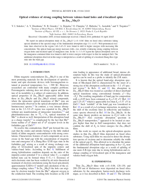
Optical evidence of strong coupling between valence-band holes and d-localized spinsin Zn1−x Mn x OV.I.Sokolov,1A.V.Druzhinin,1N.B.Gruzdev,1A.Dejneka,2O.Churpita,2Z.Hubicka,2L.Jastrabik,2and V.Trepakov2,3 1Institute of Metal Physics,UD RAS,S.Kovalevskaya Str.18,620041Yekaterinburg,Russia2Institute of Physics,AS CR,v.v.i.,Na Slovance2,18221Praha8,Czech Republic3Ioffe Institute,RAS,194021St-Petersburg,Russia͑Received3December2009;revised manuscript received2March2010;published30April2010͒We report on optical-absorption study of Zn1−x Mn x O͑x=0–0.06͒films on fused silica substrates takingspecial attention to the spectral range of the fundamental absorption edge͑3.1–4eV͒.Well-pronounced exci-tonic lines observed in the region3.40–3.45eV were found to shift to higher energies with increasing Mnconcentration.The optical band-gap energy increases with x too,reliably evidencing strong coupling betweenoxygen holes and localized spins of manganese ions.In the3.1–3.3eV region the optical-absorption curve inthe manganese-containedfilms was found to shift to lower energies with respect to that for undoped ZnO.Theadditional absorption observed in this range is interpreted as a result of splitting of a localized Zhang-Rice-typestate into the band gap.DOI:10.1103/PhysRevB.81.153104PACS number͑s͒:78.20.ϪeI.INTRODUCTIONDilute magnetic semiconductor Zn1−x Mn x O is one of themost promising materials for the development of optoelec-tronic and spin electronic devices with ferromagnetism re-tained at practical temperatures͑i.e.,Ͼ300K͒.However,researchers are confronted with many complex problems.Ferromagnetic ordering does not always appear and the na-ture of its instability is a subject of controversy.In addition,optical properties of Zn1−x Mn x O appreciably differ fromthose in Zn1−x Mn x Se and Zn1−x Mn x S related compounds,where the intracenter optical transitions of Mn2+ions areconventionally observed in the optical-absorption and photo-luminescence spectra.1,2In contrast,a very intense absorp-tion in the2.2–3.0eV region was reported in Zn1−x Mn x Owithout any manifestations of intracenter transitions,3–5and photoluminescence due to4T1→6A1optical transition of Mn2+is absent as well.Interpretation of this absorption bandas a charge transfer3,5is complicated by the fact that Mn2+forms neither d5/d4donor nor d5/d6acceptor levels in the forbidden gap of ZnO.6,7To resolve this contradiction,Dietl8put forward the con-cept that the oxides and nitrides belong to the little studiedfamily of dilute magnetic semiconductors with strong corre-lations.Characteristic features of such compounds are an in-crease in the band gap with the concentration of magneticions and emergence of a Zhang-Rice͑Z-R͒-type state in theforbidden gap9arising as a result of strong exchange cou-pling of3d-localized spin of the impurity centers andvalence-band holes.According to Ref.8,fulfillment ofstrong hybridization condition depends on the ratio of theimpurity-center potential U to a critical value U c;a coupledhybrid state can be formed when U/U cϾ1.Existence of such electronic state has been verified by ab initio theoretical treatment of electron correlations using the local spin-density approximation͑LSDA+U model͒and calculation of the ex-change coupling values.10In Zn1−x Mn x O the hole can origi-nate by electron transfer from the Mn2+adjacent oxygen to the conduction band.The resulting hole localizes as the Z-R state leading to appearance of additional broad,intense ab-sorption band.In this way the study of optical-absorptionspectra can be used as a probe to identify the Z-R states.It is known that the optical band-edge absorption spec-trum of Mn-doped ZnO is characterized by the onset of astrong rise of the absorption coefficient in theϳ3.1eV spec-tral region.11In Refs.11and12,this absorption inZn1−x Mn x Ofilms was treated as a product of direct interbandoptical transitions using conventional formula␣2ϳ͑ប−E g͒.The resulting magnitudes of band gap for composition with x=0.05have been estimated as E g=3.10eV͑Ref.11͒and3.25eV,12which is appreciably less than E g=3.37eV inZnO.13Such“redshift”of the band gap was considered inRef.12as a result of p-d exchange interaction,in analogy tothe shift of the excitonic lines in reflectivity and lumines-cence spectra observed in Ref.14for Zn1−x Mn x Se.At thesame time theory predicts an increase in E g͑x͒with x for Zn1−x Mn x O.8Also excitonic absorption spectrum in Zn1−x Mn x O nanopowders,15appeared to be located at ener-gies higher than that in ZnO nanopowders,that does not confirm the shift of E g to lower energies for Zn1−x Mn x O films.In this work we report on the optical-absorption spectrastudies in thin Zn1−x Mn x Ofilms deposited on fused silicaing suchfilms we succeed to detect the absorp-tion spectra of excitons and to determine reliably the widthof the optical gap E g.This allowed us to elucidate the natureof the additional absorption band appearing atបϽE g near the fundamental absorption edge as a result of splitting of one more Z-R-type state due to strong hybridization and ex-change coupling of3d-localized spin of the manganese and valence-band oxygen hole.II.EXPERIMENTALThin Zn1−x Mn x Ofilms with x=0–0.06,120–130,and 200–250nm of thicknesses were deposited on fused silica substrates by the atmospheric barrier-torch discharge tech-nique,as it was described in Refs.16and17.The substratePHYSICAL REVIEW B81,153104͑2010͒temperature during deposition was kept at ϳ200°C.Mn content was controlled by measurements of Mn and Zn emis-sion ͑em =4031Åand 4810Å,respectively ͒of plasma during deposition and crosschecked by the postgown EPMA ͑JEOL JXA-733device with Kevex Delta Class V mi-croanalyser ͒analysis with accuracy Ϯ0.3%.X-ray diffrac-tion ͑XRD ͒studies were performed with a Panalytical X’PertMRD Pro diffractometer with Eulerian cradle using Cu K ␣radiation ͑em =1.5405Å͒in the parallel beam ge-ometry.XRD profiles were fitted with the Pearson VII func-tion by the DIFPATAN code.18Correction for instrumental broadening was performed using NIST LaB6standard and V oigt function method.19Optical absorption within the 1.2–6.5eV spectral region was measured in unpolarized light at room temperature using a Shimadzu UV-2401PC spectrophotometer.The bare silica substrate and Zn 1−x Mn x O film on silica substrate were mounted into the reference and test channel,respectively.The optical density ␣d ͑product of optical-absorption coeffi-cient and film thickness ͒was calculated without taking into account multiple reflections as ␣d =ln ͑I 0/I ͒,where I 0and I are intensities of light passed through bare substrate and film/substrate structure.III.RESULTS AND DISCUSSIONFigure 1presents XRD pattern for ZnO and Zn 0.95Mn 0.05O films,as an example.All obtained films re-vealed crystalline block structure with dominant ͑002͒orien-tation of blocks’optical C -axes aligned normal to substrate.Observed reflexes correspond to wurtzite structure evi-dencing absence of extraneous phases.Both pure and Mn-doped ZnO films appeared to be compressively strained with 0.2%of strain,s =͑a 0−a S ͒/a 0,where a 0and a S are the lattice parameters of nonstrained and strained films.The analysis reveals that the value of compressive strain is controlled pre-dominantly by stresses,but not by presence of Mn ͑at least for Mn concentrations used ͒.Figure 2presents the optical-absorption spectra for Zn 1−x Mn x O films.A wide absorption line is seen in the re-gion of the band edge ͑Fig.2͒,whose energy appears to be shifted by about 100meV to higher energies in comparison with the excitonic line in ZnO ͓ϳ3.31eV at T =300K ͑Ref.13͔͒.The line shift is very likely connected with the com-pressive strain of Zn 1−x Mn x O films mentioned above.The wide and shifted line has been observed earlier in ZnO film on sapphire substrate 20,21and was identified as a shift of the excitonic line due to compressive strain of Zn 1−x Mn x O films.21The inset represents spectra of this line obtained in ZnO at T =300K and 77.3K.It is seen that the excitonic line is narrowed,split into two components and shifted to higher energies on lowering the temperature,clearly evidenc-ing its excitonic nature.The first line is a sum of A and B excitons,the second one is the C exciton appearing due to disorientation of blocks forming the film.16Analogous tem-perature evolutions have been reported for a wide excitonic line in ZnO nanocrystals.15As the concentration of Mn impurity increases,the exci-tonic line additionally broadens and shifts to higher energies.Figure 3shows the actual Mn concentration shift of the ex-citonic line energy បexc .It is seen that the increase in Mn concentration leads to not only changes in the excitonic spec-trum but also exhibits enhancement of the band-gap energy in Zn 1−x Mn x O films ͑band-gap magnitude can be estimated as E g =បexc +E exc ,where E exc =60meV is the excitonic binding energy 13͒.It is known that the band-gap magnitude in ZnO-MnO system varies from 3.37eV in ZnO up to 3.8eV in MnO.22According to the theoretical analysis 8per-formed taking into account inversion of ⌫7and ⌫9valence subbands in ZnO,23,24strong coupling of manganese spin and p states of valence band leads to appearance of a positiveI n t e n s i t y (c o u n t )2θ(degree)FIG.1.XRD pattern of ZnO ͑left scale ͒and Zn 0.95Mn 0.05O ͑right scale ͒films.E n e r g y (eV)αdFIG.2.Exciton absorption spectra of compressed Zn 1−x Mn x O films:1—x =0%,2—x =1.8%,and 3—x =5%;film thickness:d =͑120–130͒nm;and T =300K.Inset shows excitonic absorption lines for compressed ZnO:1—T =300K and 4—T =77.3K.01234563.403.413.423.433.44E n e r g y (e V )X (%)FIG.3.Mn-concentration dependence of the excitonic line en-ergies for Zn 1−x Mn x O films.additive in optical absorption of Zn 1−x Mn x O at small x val-ues.The sum of two contributions at sufficiently small x results in an increase in E g magnitude.The rise of the band-gap magnitude with the admixture of the second component E g ͑x ͒has been observed in Zn 1−x Co x O ͑Ref.25͒for exci-tonic lines registered in the reflection spectra at 1.6K.The shift of the excitonic line to higher energies was observed in Zn 0.99Fe 0.01O,too.20In the case of weak d -p coupling the additive into the band gap change appeared to be negative.8In this case the band-gap value E g decreases with x for x Յ0.1,as it was found for Zn 1−x Mn x Se ͑Fig.6in Ref.14͒and for Cd 1−x Mn x S.26Therefore,the observed rise of the E g ͑x ͒value with Mn addition provides the reliable experimental proof that the strong hybridization condition U /U c Ͼ1in Zn 1−x Mn x O is fulfilled.Figure 4presents optical absorption in Zn 1−x Mn x O films recorded in the spectral region 3.1–3.3eV .It is seen that the onset of optical absorption in Zn 1−x Mn x O films emerges at lower energies than that for ZnO ones.Analogous shift had been observed earlier in the spectrum of the photoluminescence excitation over deep im-purity centers in Zn 1−x Mn x O for Ref.15.Unlike authors of Refs.11and 12,we assume that addi-tional absorption of Zn 1−x Mn x O ͑in comparison with ZnO ͒in the 3.1–3.3eV range is a result of pushing the Z-R-type states out of valence band to the forbidden gap.9The essence of this state consists of localization of the valence-band hole within the first coordination sphere on the oxygen ions as a result of strong exchange interaction of manganese and hole spins.Such electronic state is similar to the Z-R-type state originally considered for La 2CuO 4oxidesuperconductor.9This state is a singlet one,because in La 2CuO 4the spins of d 9configuration of Cu 2+ion and oxy-gen holes are equal but of opposite direction.The situation is more complex in the case of Zn 1−x Mn x O since the top of valence band is formed by three close subbands:⌫7,⌫9,and ⌫7.23,24In such case we have serious reasons to assume that not only the presence of one deep Z-R-type state is respon-sible for optical absorption in the 2.2–3.0eV spectral region.We assume the presence of another,relatively shallow Z-R-type state too,which has been split off into the gap providing additional absorption in the 3.1–3.3eV region of Zn 1−x Mn x O.Tentatively,using results 11,12,15we estimate the splitting of the second Z-R level from the valence band as 0.12–0.27eV .More reliable determination of the split energy can be performed using more sensitive methods of absorp-tion spectra, e.g.,modulation methods,which are in progress.IV .CONCLUSIONThin Zn 1−x Mn x O films ͑x =0–0.06͒have been sintered and their optical-absorption spectra were investigated.The well-pronounced excitonic absorption lines in the fundamen-tal absorption spectral regions were observed.Position of excitonic absorption lines in Zn 1−x Mn x O films shifts to higher energies with increasing Mn content.This evidences an increase in the E g magnitude with x for small values x and reliably corroborates fulfillment of the strong coupling crite-rion ͑U /U c Ͼ1͒in Zn 1−x Mn x O.The last effect leads to emer-gence of an intense optical-absorption band in the 2.2–3.0eV region due to the presence of the band-gap Z-R-type state.The additional absorption observed in the range of 3.1–3.3eV is interpreted as a result of splitting of one more Z-R-type states into the band gap.ACKNOWLEDGMENTSAuthors thank T.Dietl,V .I.Anisimov,and A.V .Lukoy-anov for useful discussions and V .Valvoda for kind assis-tance in XRD experiments.This work was supported by Czech Grants No.A V0Z10100522of A V CR,No.KJB100100703of GA A V ,No.202/09/J017of GA CR,No.KAN301370701of A V CR,and No.1M06002of MSMT CR and Russian Grants No.08-02-99080r-ofiof RFBR,PP RAS “Quantum Physics of Condensed Matter”,and State Contract No.5162.nger and H.J.Richter,Phys.Rev.146,554͑1966͒.2T.Hoshina and H.Kawai,Jpn.J.Appl.Phys.19,267͑1980͒.3F.W.Kleinlein and R.Helbig,Z.Phys.266,201͑1974͒.4R.Beaulac,P.I.Archer,and D.R.Gamelin,J.Solid State Chem.181,1582͑2008͒.5T.Fukumura,Z.Jin,A.Ohtomo,H.Koinuma,and M.Kawasaki,Appl.Phys.Lett.75,3366͑1999͒.6K.A.Kikoin and V .N.Fleurov,Transition Metal Impurities in Semiconductors:Electronic Structure and Physical Properties ͑World Scientific,Singapore,1994͒,p.349.7T.Dietl,J.Magn.Magn.Mater.272-276,1969͑2004͒.8T.Dietl,Phys.Rev.B 77,085208͑2008͒.9F.C.Zhang and T.M.Rice,Phys.Rev.B 37,3759͑1988͒.10T.Chanier,F.Virot,and R.Hayn,Phys.Rev.B 79,205204͑2009͒.11V .Shinde,T.Gujar,C.Lokhande,R.Mane,and S.-H.Han,3.1253.2500.00.40.8αdEnergy (eV)12FIG.4.Spectral dependence of the optical density ␣d in the 3.1–3.3eV spectral region for Zn 1−x Mn x O,1—ZnO;2—x =0.3–0.5%;film thickness 200–250nm;and T =300K.Mater.Chem.Phys.96,326͑2006͒.12Y.Guo,X.Cao,n,C.Zhao,X.Hue,and Y.Song,J.Phys. Chem.C112,8832͑2008͒.13Zh.L.Wang,J.Phys.:Condens.Matter16,R829͑2004͒.14R.B.Bylsma,W.M.Becker,J.Kossut,U.Debska,and D. Yoder-Short,Phys.Rev.B33,8207͑1986͒.15V.I.Sokolov,A.Ye.Yermakov,M.A.Uimin,A.A.Mysik,V.A.Pustovarov,M.V.Chukichev,and N.B.Gruzdev,J.Lumin.129,1771͑2009͒.16M.Chichina,Z.Hubichka,O.Churpita,and M.Tichy,Plasma Processes Polym.2,501͑2005͒.17Z.Hubicka,M.Cada,M.Sicha,A.Churpita,P.Pokorny,L. Soukup,and L.Jastrabík,Plasma Sources Sci.Technol.11,195͑2002͒.18http://www.xray.cz/priv/kuzel/dofplatan/19R.Kuzel,Jr.,R.Cerny,V.Valvoda,and M.Blomberg,ThinSolid Films247,64͑1994͒.20Z.Jin,T.Fukumura,M.Kaasaki,K.Ando,H.Saito,T.Skiguchi, Y.Z.Yoo,M.Murakami,Y.Matsumoto,T.Hasegawa,and H. Koinuma,Appl.Phys.Lett.78,3824͑2001͒.21J.-M.Chauveau,J.Vives,J.Zuniga-Perez,ügt,M.Teis-seire,C.Deparis,C.Morhain,and B.Vinter,Appl.Phys.Lett.93,231911͑2008͒.d and V.E.Henrich,Phys.Rev.B38,10860͑1988͒. 23K.Shindo,A.Morita,and H.Kamimura,J.Phys.Soc.Jpn.20, 2054͑1965͒.24W.Y.Liang and A.D.Yoffe,Phys.Rev.Lett.20,59͑1968͒. 25W.Pacuski,D.Ferrand,J.Gibert,C.Deparis,J.A.Gaj,P.Ko-ssacki,and C.Morhain,Phys.Rev.B73,035214͑2006͒.26M.Ikeda,K.Itoh,and H.Sato,J.Phys.Soc.Jpn.25,455͑1968͒.。
mott–hubbard分裂的能带结构

mott–hubbard分裂的能带结构Mott-Hubbard分裂是指在某些材料中,由于电子间的库伦相互作用导致的能带分裂现象。
这种分裂的能带结构对材料的电子传导性质和磁性质具有重要影响。
本文将对Mott-Hubbard分裂的能带结构进行详细介绍。
让我们来了解一下Mott-Hubbard分裂的原理。
在一些过渡金属氧化物等材料中,电子的运动受到强烈的库伦相互作用的影响。
当材料中的电子密度较高时,电子间的库伦排斥力会减小能带宽度,使电子能级更加局域化。
这种局域化使得电子在材料中无法自由移动,从而抑制了电子的传导性质。
Mott-Hubbard分裂也会导致能带结构的分裂。
在材料中,电子通过与晶格相互作用形成所谓的Wannier态。
当电子的局域化程度增加时,这些Wannier态会出现能级的分裂,即Mott-Hubbard分裂。
分裂后的能带结构会出现新的能级,形成带隙。
这种带隙对电子的传导性质起到了重要的限制作用。
Mott-Hubbard分裂的能带结构对材料的电子传导性质有着重要影响。
由于带隙的存在,电子在能带中存在能量障碍,因此难以自由传导。
这使得材料的电阻率增加,电流在材料中的传输受到阻碍。
因此,Mott-Hubbard分裂的材料通常具有较高的电阻率,表现出绝缘体或半导体的特性。
Mott-Hubbard分裂也会对材料的磁性质产生影响。
在一些材料中,电子自旋与晶格自旋相互作用,形成所谓的交换相互作用。
当电子的局域化程度增加时,交换相互作用也会增强,从而导致材料出现磁性。
这种磁性可能是铁磁性、反铁磁性或顺磁性,具体取决于材料的性质。
总结起来,Mott-Hubbard分裂的能带结构是由于电子间的库伦相互作用导致的能级分裂现象。
这种分裂限制了电子的传导性质,使材料呈现出绝缘体或半导体的特性。
同时,Mott-Hubbard分裂也会影响材料的磁性质。
通过对Mott-Hubbard分裂的研究,我们可以更好地理解材料的电子结构和传导性质,为材料的设计和应用提供理论基础。
Observation of long-lived interlayer excitons in monolayer MoSe2–WSe2 heterostructures
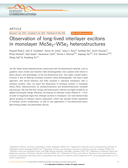
ARTICLEReceived1Apr2014|Accepted9Jan2015|Published24Feb2015Observation of long-lived interlayer excitonsin monolayer MoSe2–WSe2heterostructuresPasqual Rivera1,John R.Schaibley1,Aaron M.Jones1,Jason S.Ross2,Sanfeng Wu1,Grant Aivazian1,Philip Klement1,Kyle Seyler1,Genevieve Clark2,Nirmal J.Ghimire3,4,Jiaqiang Yan4,5,D.G.Mandrus3,4,5, Wang Yao6&Xiaodong Xu1,2Van der Waals bound heterostructures constructed with two-dimensional materials,such asgraphene,boron nitride and transition metal dichalcogenides,have sparked wide interest indevice physics and technologies at the two-dimensional limit.One highly coveted hetero-structure is that of differing monolayer transition metal dichalcogenides with type-II bandalignment,with bound electrons and holes localized in individual monolayers,that is,interlayer excitons.Here,we report the observation of interlayer excitons in monolayerMoSe2–WSe2heterostructures by photoluminescence and photoluminescence excitationspectroscopy.Wefind that their energy and luminescence intensity are highly tunable by anapplied vertical gate voltage.Moreover,we measure an interlayer exciton lifetime of B1.8ns,an order of magnitude longer than intralayer excitons in monolayers.Our work demonstratesoptical pumping of interlayer electric polarization,which may provoke further explorationof interlayer exciton condensation,as well as new applications in two-dimensional lasers,light-emitting diodes and photovoltaic devices.1Department of Physics,University of Washington,Seattle,Washington98195,USA.2Department of Materials Science and Engineering,University of Washington,Seattle,Washington98195,USA.3Department of Physics and Astronomy,University of T ennessee,Knoxville,T ennessee37996,USA.4Materials Science and T echnology Division,Oak Ridge National Laboratory,Oak Ridge,T ennessee37831,USA.5Department of Materials Science and Engineering,University of T ennessee,Knoxville,T ennessee37996,USA.6Department of Physics and Center of Theoretical and Computational Physics, University of Hong Kong,Hong Kong,China.Correspondence and requests for materials should be addressed to P.R.(email:pasqual@)or to X.X. (email:xuxd@).T he recently developed ability to vertically assemble different two-dimensional(2D)materials heralds a newrealm of device physics based on van der Waals heterostructures(HSs)1.The most successful example to date is the vertical integration of graphene on boron nitride.Such novel HSs not only markedly enhance graphene’s electronic properties2, but also give rise to superlattice structures demonstrating exotic physical phenomena3–5.A fascinating counterpart to gapless graphene is a class of monolayer direct bandgap semiconductors, namely transition metal dichalcogenides(TMDs)6–8.Due to the large binding energy in these2D semiconductors,excitons dominate the optical response,exhibiting strong light–matter interactions that are electrically tunable9,10.The discovery of excitonic valley physics11–15and strongly coupled spin and pseudospin physics16,17in2D TMDs opens up new possibilities for device concepts not possible in other material systems. Monolayer TMDs have the chemical formula MX2where the M is tungsten(W)or molybdenum(Mo),and the X is sulfur(S) or selenium(Se).Although these TMDs share the same crystalline structure,their physical properties,such as bandgap,exciton resonance and spin–orbit coupling strength,can vary signifi-cantly.Therefore,an intriguing possibility is to stack different TMD monolayers on top of one another to form2D HSs.First-principle calculations show that heterojunctions formed between monolayer tungsten and molybdenum dichalcogenides have type-II band alignment18–20.Recently,this has been confirmed by X-ray photoelectron spectroscopy and scanning tunnelling spectroscopy21.Since the Coulomb binding energy in2D TMDs is much stronger than in conventional semiconductors, it is possible to realize interlayer excitonic states in van der Waals bound heterobilayers,that is,bound electrons and holes that are localized in different layers.Such interlayer excitons have been intensely pursued in bilayer graphene for possible exciton condensation22,but direct optical observation demonstrating the existence of such excitons is challenging owing to the lack of a sizable bandgap in graphene.Monolayer TMDs with bandgaps in the visible range provide the opportunity to optically pump interlayer excitons,which can be directly observed through photoluminescence(PL)measurements.In this report,we present direct observation of interlayer excitons in vertically stacked monolayer MoSe2–WSe2HSs.We show that interlayer exciton PL is enhanced under optical excitation resonant with the intralayer excitons in isolated monolayers,consistent with the interlayer charge transfer resulting from the underlying type-II band structure.We demonstrate the tuning of the interlayer exciton energy by applying a vertical gate voltage,which is consistent with the permanent out-of-plane electric dipole nature of interlayer excitons.Moreover,wefind a blue shift in PL energy at increasing excitation power,a hallmark of repulsive dipole–dipole interac-tions between spatially indirect excitons.Finally,time-resolved PL measurements yield a lifetime of1.8ns,which is at least an order of magnitude longer than that of intralayer excitons.Our work shows that monolayer semiconducting HSs are a promising platform for exploring new optoelectronic phenomena.ResultsMoSe2–WSe2HS photoluminescence.HSs are prepared by standard polymethyl methacrylate(PMMA)transfer techniques using mechanically exfoliated monolayers of WSe2and MoSe2(see Methods).Since there is no effort made to match the crystal lattices of the two monolayers,the obtained HSs are considered incom-mensurate.An idealized depiction of the vertical MoSe2–WSe2HS is shown in Fig.1a.We have fabricated six devices that all show similar results as those reported below.The data presented here are from two independent MoSe2–WSe2HSs,labelled device1and device2.Figure1b shows an optical micrograph of device1,which has individual monolayers,as well as a large area of vertically stacked HS.This device architecture allows for the comparison of the excitonic spectrum of individual monolayers with that of the HS region,allowing for a controlled identification of spectral changes resulting from interlayer coupling.We characterize the MoSe2–WSe2monolayers and HS using PL measurements.Inspection of the PL from the HS at room temperature reveals three dominant spectral features(Fig.1c). The emission at1.65and1.57eV corresponds to the excitonic states from monolayer WSe2and MoSe2(refs10,15),respectively. PL from the HS region,outlined by the dashed white line in Fig.1a,reveals a distinct spectral feature at1.35eV(X I).Two-dimensional mapping of the spectrally integrated PL from X I shows that it is isolated entirely to the HS region(inset,Fig.1c), with highly uniform peak intensity and spectral position (Supplementary Materials1).Low-temperature characterization of the HS is performed with 1.88eV laser excitation at20K.PL from individual monolayer WSe2(top),MoSe2(bottom)and the HS area(middle)are shown with the same scale in Fig.1d.At low temperature,the intralayer neutral(X M o)and charged(X MÀ)excitons are resolved10,15,where M labels either W or parison of the three spectra shows that both intralayer X M o and X MÀexist in the HS with emission at the same energy as from isolated monolayers,demonstrating the preservation of intralayer excitons in the HS region.PL from X I becomes more pronounced and is comparable to the intralayer excitons at low temperature.We note that the X I energy position has variation across the pool of HS samples we have studied (Supplementary Fig.1),which we attribute to differences in the interlayer separation,possibly due to imperfect transfer and a different twisting angle between monolayers.We further perform PL excitation(PLE)spectroscopy to investigate the correlation between X I and intralayer excitons.A narrow bandwidth(o50kHz)frequency tunable laser is swept across the energy resonances of intralayer excitons(from1.6to 1.75eV)while monitoring X I PL response.Figure2a shows an intensity plot of X I emission as a function of photoexcitation energy from device2.We clearly observe the enhancement of X I emission when the excitation energy is resonant with intralayer exciton states(Fig.2b).Now we discuss the origin of X I.Since X I has never been observed in our exfoliated monolayer and bilayer samples,if its origin were related to defects,they must be introduced by the fabrication process.This would result in sample-dependent X I properties with non-uniform spatial dependence.However,our data show that key physical properties of X I,such as the resonance energy and intensity,are spatially uniform and isolated to the HS region(inset of Fig.1c and Supplementary Fig.2).In addition,X I has not been observed in WSe2–WSe2homo-structures constructed from exfoliated or physical vapor deposi-tion(PVD)grown monolayers(Supplementary Fig.3).All these facts suggest that X I is not a defect-related exciton.Instead,the experimental results support the observation of an interlayer exciton.Due to the type-II band alignment of the MoSe2–WSe2HS18–20,as shown in Fig.2c,photoexcited electrons and holes will relax(dashed lines)to the conduction band edge of MoSe2and the valence band edge of WSe2,respectively.The Coulomb attraction between electrons in the MoSe2and holes in the WSe2gives rise to an interlayer exciton,X I,analogous to spatially indirect excitons in coupled quantum wells.The interlayer coupling yields the lowest energy bright exciton in the HS,which is consistent with the temperature dependence of X I PL,that is,it increases as temperature decreases (Supplementary Fig.4).From the intralayer and interlayer exciton spectral positions,we can infer the band offsets between the WSe 2and MoSe 2monolayers (Fig.2c).The energy difference between X W and X I at room temperature is 310meV.Considering the smaller binding energy of interlayer than intralayer excitons,this sets a lower bound on the conduction band offset.The energy difference between X M and X I then provides a lower bound on the valence band offset of 230meV.This value is consistent with the valence band offset of 228meV found in MoS 2–WSe 2HSs by micro X-ray photoelectron spectroscopy and scanning tunnelling spectro-scopy measurements 21.This experimental evidence strongly corroborates X I as an interlayer exciton.The observation of bright interlayer excitons in monolayer semiconducting HSs is of central importance,and the remainder of this paper will focus on their physical properties resulting from their spatially indirect nature and the underlying type-II band alignment.WSe 2HSMoSe 2W M SeIn te n s i t y (a .u .)1.31.51.7Energy (eV)MoSe 2HeterostructureWSe 2W0WX X X X −0MoMo−e hehe h1.3 1.41.51.6 1.7I n t e n s i t y (a .u .)Energy (eV)5μm 0123×104Y (μm )246X (μm)0246Figure 1|Intralayer and interlayer excitons of a monolayer MoSe 2–WSe 2vertical heterostructure.(a )Cartoon depiction of a MoSe 2–WSe 2heterostructure (HS).(b )Microscope image of a MoSe 2–WSe 2HS (device 1)with a white dashed line outlining the HS region.(c )Room-temperature photoluminescence of the heterostructure under 20m W laser excitation at 2.33eV.Inset:spatial map of integrated PL intensity from the low-energy peak (1.273–1.400eV),which is only appreciable in the heterostructure area,outlined by the dashed black line.(d )Photoluminescence of individual monolayers and the HS at 20K under 20m W excitation at 1.88eV (plotted on the samescale).Energy (eV)WSe MoSe PL energy (eV)E x c i t a t i o n e n e r g y (e V )1.28 1.3 1.32 1.34 1.36 1.381.61.651.71.754,0006,0008,00010,000IntensityFigure 2|Photoluminescence excitation spectroscopy of the interlayer exciton at 20K.(a )PLE intensity plot of the heterostructure region with an excitation power of 30m W and 5s charge-coupled device CCD integration time.(b )Spectrally integrated PLE response (red dots)overlaid on PL (black line)with 100m W excitation at 1.88eV.(c )Type-II semiconductor band alignment diagram for the 2D MoSe 2–WSe 2heterojunction.interlayer exciton .Applying vertical energy of Figure 3a contact stacked insu-Electrostatic contact shows the 100to about analogue of reversed,varied expected for from reduces device 2,conduction 3b,c.of the in the on top band-offset at X I PL energy of basis of would should have X I PL This effect,intensity.further Power dependence and lifetime of interlayer exciton PL .The interlayer exciton PLE spectrum as a function of laser power with excitation energy in resonance with X W o reveals several properties of the X I .Inspection of the normalized PLE intensity (Fig.4a)shows the evolution of a doublet in the interlayer excitonspectrum,highlighted by the red and Both peaks of the doublet display a consistent increased laser intensity,shown by the dashed which are included as a guide to the eye.intensity of X I also exhibits a strong saturation laser power,as shown in Fig.4b (absolute Supplementary Fig.6).The sublinear power excitation powers above 0.5m W is distinctly the intralayer excitons in isolated monolayers,saturation power threshold of about Fig.7).The low power saturation of X I PL lifetime than that of intralayer excitons.the intralayer exciton is substantially reduced interlayer charge hopping 23,which is quenching of intralayer exciton PL (Fig.Fig.8).Moreover,the lifetime of the interlayer because it is the lowest energy configuration indirect nature leads to a reduced optical long lifetime is confirmed by time-resolved Fig.4c.A fit to a single exponential decay exciton lifetime of 1.8±0.3ns.This timescale the intralayer exciton lifetime,which is ps 24–27.By modelling the saturation behaviour three-level diagram,the calculated saturation interlayer exciton is about 180times (Supplementary Fig.7;Supplementary with our observation of low saturation intensity DiscussionWe attribute the observed doublet feature splitting of the monolayer MoSe 2conduction assignment is mainly based on the fact difference between the doublet is B 25with MoSe 2conduction band splitting predicted calculations 28.This explanation is also supported by the evolution of the relative strength of the two peaks with increasing excitation power,as shown in Fig.4a (similar results in device 1with 1.88eV excitation shown in Supplementary Fig.9).At low power,the lowest energy configuration of interlayer excitons,with the electron in the lower spin-split band of MoSe 2,is populated first.Due to phase space filling effects,the interlayer excitonSiO 2n + Si2MoSe 2e –h +e –h +P Ee –h +V g < 0WSe 2MoSe 2WSe 2MoSe 2h ωV g = 0Photon energy (eV)1.321.361.41.444080e –h +h +PL intensity (a.u.) -hω’-the interlayer exciton and band alignment.(a )Device 2geometry.The interlayer exciton has a out-of-plane electric polarization.(b )Electrostatic control of the band alignment and the interlayer exciton photoluminescence as a function of applied gate voltage under 70m W excitation at 1.744eV,1s integrationconfiguration with the electron in the higher energy spin-split band starts to be filled at higher laser power.Consequently,the higher energy peak of the doublet becomes more prominent at higher excitation powers.The observed blue shift of X I as the excitation power increases,indicated by the dashed arrows in Fig.4a,is a signature of the repulsive interaction between the dipole-aligned interlayer excitons (cf.Fig.3a).This is a hallmark of spatially indirect excitons in gallium arsenide (GaAs)coupled quantum wells,which have been intensely studied for exciton Bose-Einstein condensation (BEC)phenomena 29.The observation of spatially indirect interlayer excitons in a type-II semiconducting 2D HS provides an intriguing platform to explore exciton BEC,where the observed extended lifetimes and repulsive interactions are two key ingredients towards the realization of this exotic state of matter.Moreover,the extraordinarily high binding energy for excitons in this truly 2D system may provide for degenerate exciton gases at elevated temperatures compared with other material systems 30.The long-lived interlayer exciton may also lead to new optoelectronic applications,such as photovoltaics 31–34and 2D HS nanolasers.MethodsDevice fabrication .Monolayers of MoSe 2are mechanically exfoliated onto 300nm SiO 2on heavily doped Si wafers and monolayers of WSe 2onto a layer of PMMA atop polyvinyl alcohol on Si.Both monolayers are identified with an opticalmicroscope and confirmed by their PL spectra.Polyvinyl alcohol is dissolved in H 2O and the PMMA layer is then placed on a transfer loop or thin layer of poly-dimethylsiloxane (PDMS).The top monolayer is then placed in contact with the bottom monolayer with the aid of an optical microscope and micromanipulators.The substrate is then heated to cause the PMMA layer to release from the transfer media.The PMMA is subsequently dissolved in acetone for B 30min and then rinsed with isopropyl alcohol.Low-temperature PL measurements .Low-temperature measurements are con-ducted in a temperature-controlled Janis cold finger cryostat (sample in vacuum)with a diffraction-limited excitation beam diameter of B 1m m.PL is spectrally filtered through a 0.5-m monochromator (Andor–Shamrock)and detected on a charge-coupled device (Andor—Newton).Spatial PL mapping is performed using a Mad City Labs Nano-T555nanopositioning system.For PLE measurements,a continuous wave Ti:sapphire laser (MSquared—SolsTiS)is used for excitation and filtered from the PL signal using an 815-nm-long pass optical filter (Semrock).Electrostatic doping is accomplished with an indium drain contact deposited onto the monolayer WSe 2region of device 2and using the heavily doped Si as a tunable backgate.Time-resolved PL measurements .For interlayer lifetime measurements,we excite the sample with a o 200-fs pulsed Ti:sapphire laser (Coherent—MIRA).Interlayer PL is spectrally filtered through a 0.5-m monochromator (Princeton—Acton 2500),and detected with a fast time-correlated single-photon counting system composed of a fast (o 30ps full width at half maximum)single-photon avalanche detector (Micro Photon Devices—PDM series)and a picosecond event timer (PicoQuant—PicoHarp 300).References1.Geim,A.K.&Grigorieva,I.V.Van der Waals heterostructures.Nature 499,419–425(2013).2.Dean,C.R.et al.Boron nitride substrates for high-quality graphene electronics.Nat.Nanotechnol.5,722–726(2010).3.Hunt,B.et al.Massive Dirac fermions and Hofstadter butterfly in a van derWaals heterostructure.Science 340,1427–1430(2013).4.Dean,C.R.et al.Hofstadter’s butterfly and the fractal quantum Hall effect inmoire superlattices.Nature 497,598–602(2013).5.Ponomarenko,L.A.et al.Cloning of Dirac fermions in graphene superlattices.Nature 497,594–597(2013).6.Novoselov,K.S.et al.Two-dimensional atomic crystals.Proc.Natl Acad.SciUSA 102,10451–10453(2005).7.Mak,K.F.,Lee,C.,Hone,J.,Shan,J.&Heinz,T.F.Atomically thin MoS 2:anew direct-gap semiconductor.Phys.Rev.Lett.105,136805(2010).8.Splendiani,A.et al.Emerging photoluminescence in monolayer MoS 2.NanoLett.10,1271–1275(2010).MoSe2WSe 2dPhoton energy (eV)Laser power (μW)Time (ns)I n t e n s i t y (a .u .)N o r m a l i z e d P L E i n t e n s i t y (c o u n t s (μW s )–1)Power (μW)I n t e g r a t e d P L E i n t e n s i t y (C o u n t s (μW s )–1)2060404Figure 4|Power-dependent photoluminescence of interlayer exciton and its lifetime at 20K.(a )Power dependence of the interlayer exciton for 1.722eV excitation with a bi-Lorentzian fit to the 5and 100m W plots,normalized for power and charge-coupled device (CCD)integration time.(b )Spectrally integrated intensity of the interlayer exciton emission as a function of excitation power shows the saturation effect.(c )Time-resolvedphotoluminescence of the interlayer exciton (1.35eV)shows a lifetime of about 1.8ns.The dashed curve is the instrument response to the excitation laser pulse.(d )Illustration of the heterojunction band diagram,including the spin levels of the MoSe 2conduction band.The X I doublet has energy splitting equal to (o 0I Ào I )E 25meV.9.Mak,K.F.et al.Tightly bound trions in monolayer MoS2.Nat.Mater.12,207–211(2013).10.Ross,J.S.et al.Electrical control of neutral and charged excitons in amonolayer mun.4,1474(2013).11.Xiao,D.,Liu,G.-B.,Feng,W.,Xu,X.&Yao,W.Coupled spin and valleyphysics in monolayers of MoS2and other group-VI dichalcogenides.Phys.Rev.Lett.108,196802(2012).12.Cao,T.et al.Valley-selective circular dichroism of monolayer molybdenummun.3,887(2012).13.Zeng,H.,Dai,J.,Yao,W.,Xiao,D.&Cui,X.Valley polarization inMoS2monolayers by optical pumping.Nat.Nanotechnol.7,490–493(2012).14.Mak,K.F.,He,K.,Shan,J.&Heinz,T.F.Control of valley polarization inmonolayer MoS2by optical helicity.Nat.Nanotechnol.7,494–498(2012). 15.Jones,A.M.et al.Optical generation of excitonic valley coherence inmonolayer WSe2.Nat.Nanotechnol.8,634–638(2013).16.Gong,Z.et al.Magnetoelectric effects and valley-controlled spin quantumgates in transition metal dichalcogenide mun.4,2053(2013).17.Jones,A.M.et al.Spin-layer locking effects in optical orientation of excitonspin in bilayer WSe2.Nat.Phys.10,130–134(2014).18.Kang,J.,Tongay,S.,Zhou,J.,Li,J.&Wu,J.Band offsets and heterostructuresof two-dimensional semiconductors.Appl.Phys.Lett.102,012111–012114 (2013).19.Kos´mider,K.&Ferna´ndez-Rossier,J.Electronic properties of the MoS2-WS2heterojunction.Phys.Rev.B87,075451(2013).20.Terrones,H.,Lopez-Urias,F.&Terrones,M.Novel hetero-layered materialswith tunable direct band gaps by sandwiching different metal disulfides and diselenides.Sci.Rep.3,1549(2013).21.Chiu,M.-H.et al.Determination of band alignment in transition metaldichalcogenide heterojunctions,Preprint at http://arXiv:1406.5137(2014). 22.Su,J.-J.&MacDonald,A.H.How to make a bilayer exciton condensateflow.Nat.Phys.4,799–802(2008).23.Hong,X.P.et al.Ultrafast charge transfer in atomically thin MoS2/WS2heterostructures.Nat.Nanotechnol.9,682–686(2014).24.Wang,G.et al.Valley dynamics probed through charged and neutral excitonemission in monolayer WSe2.Phys.Rev.B90,075413(2014).garde,D.et al.Carrier and polarization dynamics in monolayer MoS2.Phys.Rev.Lett.112,047401(2014).26.Mai,C.et al.Many-body effects in valleytronics:direct measurement of valleylifetimes in single-layer MoS2.Nano Lett.14,202–206(2013).27.Shi,H.et al.Exciton dynamics in suspended monolayer and few-layer MoS22Dcrystals.ACS Nano7,1072–1080(2012).28.Korma´nyos,A.,Zo´lyomi,V.,Drummond,N.D.&Burkard,G.Spin-orbitcoupling,quantum dots,and qubits in monolayer transition metaldichalcogenides.Phys.Rev.X4,011034(2014).29.Butov,L.V.,Lai,C.W.,Ivanov,A.L.,Gossard,A.C.&Chemla,D.S.TowardsBose-Einstein condensation of excitons in potential traps.Nature417,47–52 (2002).30.Fogler,M.M.,Butov,L.V.&Novoselov,K.S.High-temperature superfluiditywith indirect excitons in van der Waals mun.5,4555 (2014).31.Lee,C.H.et al.Atomically thin p-n junctions with van der Waalsheterointerfaces.Nat.Nanotechnol.9,676–681(2014).32.Furchi,M.M.,Pospischil,A.,Libisch,F.,Burgdorfer,J.&Mueller,T.Photovoltaic effect in an electrically tunable van der Waals heterojunction.Nano Lett.14,4785–4791(2014).33.Cheng,R.et al.Electroluminescence and photocurrent generation fromatomically sharp WSe2/MoS2heterojunction p-n diodes.Nano Lett.14,5590–5597(2014).34.Fang,H.et al.Strong interlayer coupling in van der Waals heterostructuresbuilt from single-layer chalcogenides.Proc.Natl A111,6198–6202 (2014).AcknowledgementsThis work is mainly supported by the US DoE,BES,Materials Sciences and Engineering Division(DE-SC0008145).N.J.G.,J.Y.and D.G.M.are supported by US DoE,BES, Materials Sciences and Engineering Division.W.Y.is supported by the Research Grant Council of Hong Kong(HKU17305914P,HKU9/CRF/13G),and the Croucher Foun-dation under the Croucher Innovation Award.X.X.thanks the support of the Cottrell Scholar Award.P.R.thanks the UW GO-MAP program for their support.A.M.J.is partially supported by the NSF(DGE-0718124).J.S.R.is partially supported by the NSF (DGE-1256082).S.W.and G.C.are partially supported by the State of Washington through the UW Clean Energy Institute.Device fabrication was performed at the Washington Nanofabrication Facility and NSF-funded Nanotech User Facility. Author contributionsX.X.and P.R.conceived the experiments.P.R.and P.K.fabricated the devices,assisted by J.S.R.P.R.performed the measurements,assisted by J.R.S.,A.M.J.,J.S.R.,S.W.and G.A. P.R.and X.X.performed data analysis,with input from W.Y.N.J.G.,J.Y.and D.G.M. synthesized and characterized the bulk WSe2crystals.X.X.,P.R.,J.R.S.and W.Y.wrote the paper.All authors discussed the results.Additional informationSupplementary Information accompanies this paper at / naturecommunicationsCompetingfinancial interests:The authors declare no competingfinancial interests. Reprints and permission information is available online at / reprintsandpermissions/How to cite this article:Rivera,P.et al.Observation of long-lived interlayer excitons in monolayer MoSe2–mun.6:6242doi:10.1038/ncomms7242(2015).。
Mach_数和壁面温度对HyTRV_边界层转捩的影响
第9卷㊀第2期2024年3月气体物理PHYSICSOFGASESVol.9㊀No.2Mar.2024㊀㊀DOI:10.19527/j.cnki.2096 ̄1642.1098Mach数和壁面温度对HyTRV边界层转捩的影响章录兴ꎬ㊀王光学ꎬ㊀杜㊀磊ꎬ㊀余发源ꎬ㊀张怀宝(中山大学航空航天学院ꎬ广东深圳518107)EffectsofMachNumberandWallTemperatureonHyTRVBoundaryLayerTransitionZHANGLuxingꎬ㊀WANGGuangxueꎬ㊀DULeiꎬ㊀YUFayuanꎬ㊀ZHANGHuaibao(SchoolofAeronauticsandAstronauticsꎬSunYat ̄senUniversityꎬShenzhen518107ꎬChina)摘㊀要:典型的高超声速飞行器流场存在着复杂的转捩现象ꎬ其对飞行器的性能有着显著的影响ꎮ针对HyTRV这款接近真实高超声速飞行器的升力体模型ꎬ采用数值模拟方法ꎬ研究Mach数和壁面温度对HyTRV转捩的影响规律ꎮ采用课题组自研软件开展数值计算ꎬMach数的范围为3~8ꎬ壁面温度的范围为150~900Kꎮ首先对γ ̄Re~θt转捩模型和SST湍流模型进行了高超声速修正:将压力梯度系数修正㊁高速横流修正引入到γ ̄Re~θt转捩模型ꎬ并对SST湍流模型闭合系数β∗和β进行可压缩修正ꎻ然后开展了网格无关性验证ꎬ通过与实验结果对比ꎬ确认了修正后的数值方法和软件平台ꎻ最终开展Mach数和壁面温度对HyTRV边界层转捩规律的影响研究ꎮ计算结果表明ꎬ转捩区域主要集中在上表面两侧㊁下表面中心线两侧ꎻ增大来流Mach数ꎬ上下表面转捩起始位置均大幅后移ꎬ湍流区大幅缩小ꎬ但仍会存在ꎬ同时上表面层流区摩阻系数不断增大ꎬ下表面湍流区摩阻系数不断减小ꎻ升高壁面温度ꎬ上下表面转捩起始位置先前移ꎬ然后快速后移ꎬ最终湍流区先后几乎消失ꎮ关键词:转捩ꎻHyTRVꎻ摩阻ꎻMach数ꎻ壁面温度㊀㊀㊀收稿日期:2023 ̄12 ̄13ꎻ修回日期:2024 ̄01 ̄02基金项目:国家重大项目(GJXM92579)ꎻ广东省自然科学基金-面上项目(2023A1515010036)ꎻ中山大学中央高校基本科研业务费专项资金(22qntd0705)第一作者简介:章录兴(1998 )㊀男ꎬ硕士ꎬ主要研究方向为高超声速空气动力学ꎮE ̄mail:184****8082@163.com通信作者简介:张怀宝(1985 )㊀男ꎬ副教授ꎬ主要研究方向为空气动力学ꎮE ̄mail:zhanghb28@mail.sysu.edu.cn中图分类号:V211ꎻV411㊀㊀文献标志码:AAbstract:Thereisacomplextransitionphenomenonintheflowfieldofatypicalhypersonicvehicleꎬwhichhasasignifi ̄cantimpactontheperformanceofthevehicle.TheeffectsofMachnumberandwalltemperatureonthetransitionofHyTRVwerestudiedbynumericalsimulationmethods.Theself ̄developedsoftwareoftheresearchgroupwasusedtocarryoutnu ̄mericalcalculations.TherangeofMachnumberwas3~8ꎬandtherangeofwalltemperaturewas150~900K.Firstlyꎬthehypersoniccorrectionsoftheγ ̄Re~θttransitionmodelandtheSSTturbulencemodelwerecarriedout.Thepressuregradientcoefficientcorrectionandthehigh ̄speedcross ̄flowcorrectionwereintroducedintotheγ ̄Re~θttransitionmodelꎬandthecom ̄pressibilitycorrectionsoftheclosurecoefficientsβ∗andβoftheSSTturbulencemodelwerecarriedout.Thenꎬthegridin ̄dependenceverificationwascarriedoutꎬandthemodifiednumericalmethodandsoftwareplatformwereconfirmedbycom ̄paringwithexperimentalresults.FinallyꎬtheeffectsofMachnumberandwalltemperatureonthetransitionlawoftheHyTRVboundarylayerwerestudied.Theresultsshowthatthetransitionareaismainlyconcentratedonbothsidesoftheuppersurfaceandthecenterlineofthelowersurface.WiththeincreaseoftheincomingMachnumberꎬthestartingpositionoftransitionontheupperandlowersurfacesisgreatlybackwardꎬandtheturbulentzoneisgreatlyreducedꎬbutitstillex ̄ists.Atthesametimeꎬthefrictioncoefficientofthelaminarflowzoneontheuppersurfaceincreasescontinuouslyꎬandthefrictioncoefficientoftheturbulentzoneonthelowersurfacedecreases.Asthewalltemperatureincreasesꎬthestartingposi ̄tionoftransitionontheupperandlowersurfacesshiftsforwardꎬthenrapidlyshiftsbackwardꎬandfinallytheturbulentzonealmostdisappears.气体物理2024年㊀第9卷Keywords:transitionꎻHyTRVꎻfrictionꎻMachnumberꎻwalltemperature引㊀言高超声速飞行器具有突防能力强㊁打击范围广㊁响应迅速等显著优势ꎬ正逐渐成为各国空天竞争的热点[1]ꎮ高超声速飞行器边界层转捩是该类飞行器气动设计中的重要问题[2]ꎮ在边界层转捩过程中ꎬ流态由层流转变为湍流ꎬ飞行器的表面摩阻急剧增大到层流时的3~5倍ꎬ严重影响飞行器的气动性能与热防护系统ꎬ转捩还会导致飞行器壁面烧蚀㊁颤振加剧㊁飞行姿态控制难度大等一系列问题ꎬ对飞行器的飞行安全构成严重的威胁[3 ̄5]ꎬ开展高超声速飞行器边界层转捩研究具有十分重要的意义ꎮ影响边界层转捩的因素很多ꎬ例如ꎬMach数㊁Reynolds数㊁湍流强度㊁表面传导热等ꎮ在高超声速流动条件下ꎬ强激波㊁强逆压梯度㊁熵层等高超声速现象及其相互作用ꎬ会使得转捩流动的预测和研究难度进一步增大[6]ꎮ目前高超声速飞行器转捩数值模拟方法主要有直接数值模拟(DNS)㊁大涡模拟(LES)和基于Reynolds平均Navier ̄Stokes(RANS)的转捩模型方法ꎬ由于前两种计算量巨大ꎬ难以推广到工程应用ꎬ基于Reynolds平均Navier ̄Stokes的转捩模型在工程实践中应用最为广泛ꎬ其中γ ̄Re~θt转捩模型基于局部变量ꎬ与现代CFD方法良好兼容ꎬ目前已经有多项研究尝试从一般性的流动问题拓展到高超声速流动转捩模拟[6 ̄9]ꎮ目前高超声速流动转捩的研究对象主要是结构相对简单的构型ꎮMcDaniel等[10]研究了扩口直锥在高超声速流动条件下的转捩现象ꎮPapp等[11]研究了圆锥在高超声速流动条件下的转捩特性ꎮ美国和澳大利亚组织联合实施的HIFiRE计划[12]ꎬ研究了圆锥形状的HIFiRE1和椭圆锥形的HIFiRE5的转捩问题ꎮ杨云军等[13]采用数值模拟方法ꎬ分析了椭圆锥的转捩影响机制ꎬ并研究了Reynolds数对转捩特性的影响规律ꎮ另外ꎬ袁先旭等[14]于2015年成功实施了圆锥体MF ̄1航天模型飞行试验ꎮ以上对高超声速流动的转捩研究ꎬ都取得了比较理想的结果ꎬ然而所采用的模型都是圆锥㊁椭圆锥等简单几何外形ꎬ这与真实高超声速飞行器有较大差异ꎬ较难反映真实的转捩特性ꎮ为了有效促进对真实高超声速飞行器的转捩问题研究ꎬ中国空气动力研究与发展中心提出并设计了一款接近真实飞行器的升力体模型ꎬ即高超声速转捩研究飞行器(hypersonictransitionresearchvehicleꎬHyTRV)[15]ꎬ模型详细的参数见参考文献[16]ꎮHyTRV外形如图1所示ꎬ其整体外形较为复杂ꎬ不同区域发生转捩的情况也不尽相同ꎮ对HyTRV的转捩问题研究能够显著提高对真实高超声速飞行器转捩特性的认识水平ꎮLiu等[17]采用理论分析㊁数值模拟和风洞实验3种方法对HyTRV的转捩特性进行了研究ꎻ陈坚强等[15]分析了HyTRV的边界层失稳特征ꎻChen等[18]对HyTRV进行了多维线性稳定性分析ꎻQi等[19]在来流Mach数6㊁攻角0ʎ的条件下对HyTRV进行了直接数值模拟ꎻ万兵兵等[20]结合风洞实验与飞行试验ꎬ利用eN方法预测了HyTRV升力体横流区的转捩阵面形状ꎮ目前ꎬ相关研究主要集中在HyTRV的稳定性特征及转捩预测两个方面ꎬ而对若干关键参数ꎬ特别是Mach数和壁面温度对转捩的影响研究还比较少ꎮ(a)Frontview(b)Sideview㊀㊀㊀图1㊀HyTRV外形Fig.1㊀ShapeofHyTRV基于此ꎬ本文采用数值模拟方法ꎬ应用课题组自研软件开展Mach数和壁面温度对HyTRV转捩流动的影响规律研究ꎮ1㊀数值方法1.1㊀控制方程和数值方法控制方程为三维可压缩RANS方程ꎬ采用结构网格技术和有限体积方法ꎬ变量插值方法采用2阶MUSCL格式ꎬ通量计算采用低耗散的通量向量差分Roe格式ꎬ黏性项离散采用中心格式ꎬ时间推进方法采用LU ̄SGS格式ꎮ壁面采用等温㊁无滑移壁面条件ꎬ入口采用Riemann远场边界条件ꎬ出口采用零梯度外推边界条件ꎮ1.2㊀γ ̄Re~θt转捩模型γ ̄Re~θt转捩模型是Menter等[21ꎬ22]于2004年提01第2期章录兴ꎬ等:Mach数和壁面温度对HyTRV边界层转捩的影响出的一种基于拟合公式的间歇因子转捩模型ꎬ在2009年公布了完整的拟合公式及相关参数[23]ꎮ许多学者也开发了相应的程序ꎬ并进行了大量的算例验证[24 ̄28]ꎬ证明了该模型具有较好的转捩预测能力ꎬ预测精度较高ꎻ通过合适的标定ꎬγ ̄Re~θt转捩模型可以适用于多种情况下的转捩模拟ꎮ该模型构建了关于间歇因子γ的输运方程和关于转捩动量厚度Reynolds数Re~θt的输运方程ꎮ具体来说ꎬγ表示该位置是湍流流动的概率ꎬ取值范围为0<γ<1ꎮ关于γ的控制方程为Ə(ργ)Ət+Ə(ρujγ)Əxj=Pγ-Eγ+ƏƏxjμ+μtσfæèçöø÷ƏγƏxjéëêêùûúú其中ꎬPγ为生成项ꎬEγ为破坏项ꎮ关于Re~θt的输运方程为Ə(ρRe~θt)Ət+Ə(ρujRe~θt)Əxj=Pθt+ƏƏxjσθt(μ+μt)ƏRe~θtƏxjéëêêùûúú其中ꎬPθt为源项ꎬ其作用是使边界层外部的Re~θt等于Reθtꎬ定义式为Pθt=cθtρt(Reθt-Re~θt)(1.0-Fθt)Reθt采用以下经验公式Reθt=1173.51-589 428Tu+0.2196Tu2æèçöø÷F(λθ)ꎬTuɤ0.3Reθt=331.50(Tu-0.5658)-0.671F(λθ)ꎬTu>0.3ìîíïïïïF(λθ)=1+(12.986λθ+123.66λ2θ+405.689λ3θ)e-(Tu1.5)1.5ꎬ㊀λθɤ0F(λθ)=1+0.275(1-e-35.0λθ)e-(Tu0.5)ꎬλθ>0ìîíïïïï在实际计算中ꎬ通过γ ̄Re~θt转捩模型获得间歇因子ꎬ再通过间歇因子来控制SSTk ̄ω湍流模型中湍动能的生成ꎮγ ̄Re~θt转捩模型与SSTk ̄ω湍流模型耦合为Ə(ρk)Ət+Ə(ρujk)Əxj=γeffτijƏuiƏxj-min(max(γeffꎬ0.1)ꎬ1.0)ρβ∗kω+ƏƏxjμ+μtσkæèçöø÷ƏkƏxjéëêêùûúúƏ(ρω)Ət+Ə(ρujω)Əxj=γvtτijƏuiƏxj-βρω2+ƏƏxj(μ+σωμt)ƏωƏxjéëêêùûúú+2ρ(1-F1)σω21ωƏkƏxjƏωƏxj模型中具体参数定义见文献[23]ꎮ1.3㊀高超声速修正原始SST湍流模型及γ ̄Re~θt转捩模型都是基于不可压缩流动发展的ꎬ为了更好地预测高超声速流动转捩ꎬ本节引入了3种重要的高超声速修正方法ꎮ1.3.1㊀压力梯度修正压力梯度对边界层转捩的影响较大ꎬ在高Mach数情况下ꎬ边界层厚度较大ꎬ进而影响压力梯度的大小ꎬ因此在模拟高超声速流动时应该考虑Mach数对压力梯度的影响ꎮ本文采用张毅峰等[29]提出的压力梯度修正方法ꎬ具体修正形式如下λᶄθ=λθ1+γᶄ-12Maeæèçöø÷其中ꎬMae为边界层外缘Mach数ꎬγᶄ为比热比ꎮ1.3.2㊀高速横流修正在原始γ ̄Re~θt转捩模型中ꎬ没有考虑横流不稳定性对转捩的影响ꎬ对于横流模态主导的转捩ꎬ原始转捩模型计算的结果并不理想ꎮLangtry等[30]在2015年对γ ̄Re~θt转捩模型进行了低速横流修正ꎬ向星皓等[9]在Langtry低速横流修正的基础上ꎬ对高超声速椭圆锥转捩DNS数据进行了拓展ꎬ提出了高速横流转捩判据ꎬ本文直接采用向星皓提出的高速横流转捩方法ꎮLangtry将横流强度引入转捩发生动量厚度Reynolds数输运方程中Ə(ρRe~θt)Ət+Ə(ρujRe~θt)Əxj=Pθt+DSCF+ƏƏxjσθt(μ+μt)ƏRe~θtƏxjéëêêùûúú式中ꎬDSCF为横流源项ꎬLangtry低速横流修正为DSCF=cθtρtccrossflowmin(ReSCF-Re~θtꎬ0.0)Fθt2其中ꎬReSCF为低速横流判据ReSCF=θtρUlocal0.82æèçöø÷μ=-35.088lnhθtæèçöø÷+319.51+f(+ΔHcrossflow)-f(-ΔHcrossflow)其中ꎬh为壁面粗糙度高度ꎬθt为动量厚度ꎬ11气体物理2024年㊀第9卷ΔHcrossflow是横流强度抬升项ꎮ向星皓提出的高速横流转捩判据ꎬ其中高速横流源项DSCF ̄H为DSCF ̄H=cCFρmin(ReSCF ̄H-Re~θtꎬ0)FθtReSCF ̄H=CCF ̄1lnhlμ+CCF ̄2+(Hcrossflow)其中ꎬCCF ̄1=-9.618ꎬCCF ̄2=128.33ꎻlμ为粗糙度参考高度ꎬlμ=1μmꎻf(Hcrossflow)为抬升函数f(Hcrossflow)=60000.1066-ΔHcrossflow+50000(0.1066-ΔHcrossflow)2其中ꎬΔHcrossflow与Langtry低速横流修正中保持一致ꎮ1.3.3㊀SST可压缩修正高超声速流动具有强可压缩性ꎬ所以在进行高超声速计算时ꎬ应该对湍流模型进行可压缩修正ꎮSarkar[31]提出了膨胀耗散修正ꎬ对SST湍流模型中的闭合系数β∗ꎬβ进行了可压缩修正ꎬWilcox[32]在Sarkar修正的基础上考虑了可压缩生成项产生时的延迟效应ꎬ使得可压缩修正在湍流Mach数较小的近壁面关闭ꎬ在湍流Mach数较大的自由剪切层打开ꎬ本文采用Wilcox提出的可压缩性修正β∗=β∗0[1+ξ∗F(Mat)]β=β0-β∗0ξ∗F(Mat)其中ꎬβ0ꎬβ∗均为原始模型中的系数ꎬξ∗=1.5ꎮF(Mat)=[Mat-Mat0]H(Mat-Mat0)Mat0=1/4ꎬH(x)=0ꎬxɤ01ꎬx>0{其中ꎬMat=2k/a为湍流Mach数ꎬa为当地声速ꎮ2㊀网格无关性验证及数值方法确认2.1㊀网格无关性验证计算采用3套网格ꎬ考虑到HyTRV的几何对称性ꎬ生成3套半模网格ꎬ第1层网格高度为1ˑ10-6mꎬ确保y+<1ꎬ流向ˑ法向ˑ周向的网格数分别为:网格1是301ˑ201ˑ201ꎬ网格2是301ˑ301ˑ201ꎬ网格3是401ˑ381ˑ281ꎮ全模下表面如图2所示ꎬ选取y/L=0中心线和x/L=0.5处ꎬ对比3套网格的表面摩阻系数ꎬ计算结果如图3所示ꎮ采用网格1时ꎬ表面摩阻系数分布与另外两个结果存在明显差异ꎻ而采用网格2和网格3时ꎬ表面摩阻系数曲线基本重合ꎬ表明在流向㊁法向和周向均满足网格无关性ꎬ后续数值计算采用网格2ꎮ图2㊀截取位置示意图Fig.2㊀Schematicdiagramoftheinterceptionlocation(a)Surfacefrictionaty/L=0(b)Surfacefrictionatx/L=0.5图3㊀采用3套网格计算得到的摩阻对比Fig.3㊀Comparisonofthefrictiondragcalculatedusingthreesetsofgrids2.2㊀数值方法和自研软件的确认采用修正后的转捩模型对HyTRV开展计算ꎬ计算工况为Ma=6ꎬ来流温度Tɕ=97Kꎬ单位21第2期章录兴ꎬ等:Mach数和壁面温度对HyTRV边界层转捩的影响Reynolds数为Re=1.1ˑ107/mꎬ攻角α=0ʎꎬ来流湍流度FSTI=0.8%ꎬ壁面温度T=300Kꎮ为方便对比分析ꎬ计算结果与参考结果均采用上下对称形式布置ꎬ例如ꎬ图4是模型下表面计算结果与实验结果对比:对于下表面两侧转捩的起始位置ꎬ高超声速修正前的转捩位置在x=0.68m附近ꎬ高超声速修正后的计算结果与实验结果吻合良好ꎬ均在x=0.60m附近ꎬ并且湍流边界层区域形状基本一致ꎬ说明修正后的转捩模型能够较好地预测HyTRV转捩的位置ꎮ(a)Calculationofthefrictiondistribution(beforehypersoniccorrection)(b)Calculationofthefrictiondistribution(afterhypersoniccorrection)(c)Experimentalresultsoftheheatfluxdistribution[17]图4㊀下表面计算结果和实验结果对比Fig.4㊀Comparisonofthecalculatedandexperimentalresultsonthelowersurface3㊀HyTRV转捩的基本流动特性计算工况采用Ma=6ꎬ攻角α=0ʎꎬ来流湍流度FSTI=0.6%ꎬ分析HyTRV转捩的基本流动特性ꎮ从图5可以看出ꎬ模型两侧和顶端均出现高压区ꎬ高压区之间为低压区ꎬ横截面上存在周向压力梯度ꎬ流动从高压区向低压区汇集ꎬ从而在下表面中心线附近和上表面两侧腰部区域均形成流向涡结构(见图6)ꎬ沿流动方向ꎬ高压区域逐渐扩大ꎬ流向涡结构的影响范围也越大ꎮ在流向涡结构的边缘位置ꎬ壁面附近的低速流体被抬升到外壁面区域ꎬ外壁面区域的高速流体又被带入到近壁面区域ꎬ进而导致流向涡结构边缘处壁面的摩阻显著增加ꎬ最终诱发转捩ꎬ这些流动特征与文献[15]的结果一致ꎮ图7显示了上下表面摩阻的分布情况ꎬ其中上表面两侧区域在x/L=0.80附近ꎬ摩阻显著增加ꎬ出现明显的转捩现象ꎬ转捩区域分布在两侧边缘位置ꎻ而下表面两侧区域在x/L=0.75附近ꎬ也出现明显的转捩ꎬ转捩区域相对集中在中心线两侧ꎮ图5㊀不同截面位置处的压力云图Fig.5㊀Pressurecontoursatdifferentcross ̄sectionlocations图6㊀不同截面位置处的流向速度云图Fig.6㊀Streamwisevelocitycontoursatdifferentcross ̄sectionlocations31气体物理2024年㊀第9卷(a)Uppersurface㊀㊀㊀㊀㊀(b)Lowersurface图7㊀上下表面摩阻分布云图Fig.7㊀Frictioncoefficientcontoursontheupperandlowersurfaces4㊀不同Mach数对HyTRV转捩的影响保持来流湍流度FSTI=0.6%不变ꎬMach数变化范围为3~8ꎮ图8是不同Mach数条件下HyTRV上下表面的摩阻分布云图ꎬ从图中可知ꎬ随着Mach数的增加ꎬ上下表面的湍流区域均逐渐减少ꎬ其中上表面两侧转捩起始位置由x/L=0.56附近后移至x/L=0.92附近ꎬ下表面两侧转捩起始位置由x/L=0.48附近后移至x/L=0.99附近ꎬ上下表面两侧转捩起始位置均大幅后移ꎬ说明Mach数对HyTRV转捩的影响很大ꎮuppersurface㊀㊀㊀㊀㊀㊀㊀㊀㊀㊀㊀㊀㊀㊀㊀㊀lowersurface(a)Ma=3uppersurface㊀㊀㊀㊀㊀㊀㊀㊀㊀㊀㊀㊀㊀㊀㊀㊀lowersurface(b)Ma=4uppersurface㊀㊀㊀㊀㊀㊀㊀㊀㊀㊀㊀㊀㊀㊀㊀㊀lowersurface(c)Ma=541第2期章录兴ꎬ等:Mach数和壁面温度对HyTRV边界层转捩的影响uppersurface㊀㊀㊀㊀㊀㊀㊀㊀㊀㊀㊀㊀㊀㊀㊀㊀lowersurface(d)Ma=6uppersurface㊀㊀㊀㊀㊀㊀㊀㊀㊀㊀㊀㊀㊀㊀㊀㊀lowersurface(e)Ma=7uppersurface㊀㊀㊀㊀㊀㊀㊀㊀㊀㊀㊀㊀㊀㊀㊀㊀lowersurface(f)Ma=8图8㊀不同Mach数条件下摩阻系数分布云图Fig.8㊀FrictioncoefficientcontoursatdifferentMachnumbers上表面选取图7中z/L=0.12的位置ꎬ下表面选取z/L=0.10的位置进行分析ꎮ从图9中可以分析出ꎬ随着Mach数的增加ꎬ上表面转捩起始位置不断后移ꎬ当Mach数增加到7时ꎬ由于湍流区的缩小ꎬ此处位置不再发生转捩ꎬ此外ꎬMach数越高层流区摩阻系数越大ꎻ下表面转捩起始位置也不断后移ꎬ当Mach数增加到8时ꎬ此处位置不再发生转捩ꎬ此外ꎬMach数越高ꎬ湍流区的摩阻系数越小ꎬ这些结论与关于来流Mach数对转捩位置影响的普遍研究结论一致ꎮ(a)Uppersurface㊀㊀㊀㊀㊀(b)Lowersurface图9㊀不同位置摩阻系数随Mach数的变化Fig.9㊀VariationoffrictioncoefficientwithMachnumberatdifferentlocations51气体物理2024年㊀第9卷5㊀不同壁面温度对HyTRV转捩的影响保持来流湍流度FSTI=0.6%及Ma=6不变ꎬ壁面温度的变化范围为150~900Kꎮ图10是不同壁面温度条件下HyTRV上下表面的摩阻分布云图ꎬ可以看出随着壁面温度的增加ꎬ上表面两侧湍流区域先是缓慢扩大ꎬ在壁面温度为500K时湍流区域快速缩小ꎬ增加到900K时ꎬ已无明显湍流区域ꎻ下表面两侧湍流区域先是无明显变化ꎬ同样当壁面温度升高到500K时ꎬ湍流区域快速缩小ꎬ当壁面温度升高到700K时ꎬ两侧已经无明显的湍流区域ꎬ相比上表面两侧湍流区域ꎬ下表面湍流区域消失得更早ꎮ由此可以得出壁面温度对转捩的产生有较大的影响ꎬ壁面温度增加到一定程度将导致HyTRV没有明显的转捩现象ꎮuppersurface㊀㊀㊀㊀㊀㊀㊀㊀㊀㊀㊀㊀㊀㊀㊀㊀lowersurface(a)T=150Kuppersurface㊀㊀㊀㊀㊀㊀㊀㊀㊀㊀㊀㊀㊀㊀㊀㊀lowersurface(b)T=200Kuppersurface㊀㊀㊀㊀㊀㊀㊀㊀㊀㊀㊀㊀㊀㊀㊀㊀lowersurface(c)T=300Kuppersurface㊀㊀㊀㊀㊀㊀㊀㊀㊀㊀㊀㊀㊀㊀㊀㊀lowersurface(d)T=500K61第2期章录兴ꎬ等:Mach数和壁面温度对HyTRV边界层转捩的影响uppersurface㊀㊀㊀㊀㊀㊀㊀㊀㊀㊀㊀㊀㊀㊀㊀㊀lowersurface(e)T=700Kuppersurface㊀㊀㊀㊀㊀㊀㊀㊀㊀㊀㊀㊀㊀㊀㊀㊀lowersurface(f)T=900K图10㊀不同壁面温度条件下摩阻系数分布云图Fig.10㊀Frictioncoefficientcontoursatdifferentwalltemperatureconditions上表面选取z/L=0.125的位置ꎬ下表面选取z/L=0.100的位置进行分析ꎮ从图11中可以分析出ꎬ随着壁面温度的增加ꎬ上表面转捩起始位置先前移ꎬ当壁面温度增加到500K时ꎬ转捩起始位置后移ꎬ转捩区长度逐渐增加ꎬ层流区域的摩阻系数逐渐增加ꎬ当壁面温度增加到700K时ꎬ该位置已不再出现转捩ꎻ下表面转捩起始位置先小幅后移ꎬ当壁面温度增加到300K时ꎬ转捩起始位置开始后移ꎬ当壁面温度增加到700K时ꎬ由于湍流区域的减小ꎬ该位置不再发生转捩ꎮ(a)Uppersurface㊀㊀㊀㊀㊀(b)Lowersurface图11㊀不同位置摩阻系数随壁面温度的变化Fig.11㊀Variationoffrictioncoefficientwithwalltemperatureatdifferentlocations为进一步分析壁面温度的影响ꎬ本文分别在上下表面湍流区选取一点(0.9ꎬ0.029ꎬ0.14)ꎬ(0.97ꎬ-0.34ꎬ0.12)ꎬ分析边界层湍动能剖面ꎬ结果如图12所示ꎮ从图中可以看到ꎬ随着壁面温度升高ꎬ边界层厚度先略微变厚ꎬ再变薄ꎬ当壁面温度升高到700K时ꎬ边界层厚度迅速降低ꎮ这些结果与转捩位置先前移再后移的结论相符合ꎬ因为边界层厚度会影响不稳定波的时间和空间尺度ꎬ边界层厚度低时ꎬ不稳定波增长速度变慢ꎬ延迟转捩发生ꎮ需要指出的是ꎬ仅采用当前使用的方法ꎬ无法从更深层71气体物理2024年㊀第9卷次揭示转捩反转的流动机理ꎬ而须另外借助稳定性分析方法ꎬ例如ꎬ使用eN方法开展基于模态的稳定性研究ꎮ文献[33]采用该手段研究了大掠角平板钝三角翼随壁温比变化出现转捩反转的内在机理:壁温比升高促进横流模态和第1模态扰动增长ꎬ抑制第2模态发展ꎬ在第1㊁2模态联合作用影响下ꎬ出现转捩反转现象ꎮ我们将在后续开展进一步研究ꎮ(a)Uppersurface(b)Lowersurface图12㊀不同位置湍动能剖面随壁面温度的变化Fig.12㊀Variationofturbulentkineticenergywithwalltemperatureatdifferentlocations6㊀结论针对HyTRV转捩问题ꎬ在Mach数Ma=3~8ꎬ壁面温度T=150~900K的条件下ꎬ基于课题组自研软件ꎬ对γ ̄Re~θt转捩模型和SST湍流模型进行了高超声速修正ꎬ研究了Mach数和壁面温度对HyTRV转捩的影响ꎬ得出以下结论:1)经过高超声速修正后的γ ̄Re~θt转捩模型和SST湍流模型能够较为准确地预测HyTRV转捩位置ꎬ并且湍流边界层区域形状与实验结果基本一致ꎻHyTRV存在多个不同的转捩区域ꎬ上表面两侧转捩区域分布在两侧边缘位置ꎬ下表面两侧转捩区域分布在中心线两侧ꎮ2)Mach数的增加会导致上下表面转捩起始位置均大幅后移ꎬ湍流区大幅缩小ꎬ但当Mach数增加到8时ꎬ湍流区仍然存在ꎬ并没有消失ꎻ上表面层流区摩阻不断增加ꎬ下表面湍流区摩阻不断减小ꎮ3)壁面温度的增加会导致上下表面转捩起始位置先前移ꎬ再后移ꎬ这与边界层厚度变化规律一致ꎬ当壁面温度增加到700K时ꎬ下表面湍流区已经基本消失ꎬ当壁面温度增加到900K时ꎬ上表面湍流区也基本消失ꎻ上表面在层流区域的摩阻系数逐渐增大ꎬ在湍流区的摩阻系数逐渐减小ꎮ致谢㊀感谢中国空气动力研究与发展中心和空天飞行空气动力科学与技术全国重点实验室提供的HyTRV模型数据和实验数据ꎮ参考文献(References)[1]㊀OberingIIIHꎬHeinrichsRL.Missiledefenseforgreatpowerconflict:outmaneuveringtheChinathreat[J].Stra ̄tegicStudiesQuarterlyꎬ2019ꎬ3(4):37 ̄56. [2]ChengCꎬWuJHꎬZhangYLꎬetal.Aerodynamicsanddynamicstabilityofmicro ̄air ̄vehiclewithfourflappingwingsinhoveringflight[J].AdvancesinAerodynamicsꎬ2020ꎬ2(3):5.[3]BertinJJꎬCummingsRM.Fiftyyearsofhypersonics:whereweᶄvebeenꎬwhereweᶄregoing[J].ProgressinAerospaceSciencesꎬ2003ꎬ39(6/7):511 ̄536. [4]陈坚强ꎬ涂国华ꎬ张毅锋ꎬ等.高超声速边界层转捩研究现状与发展趋势[J].空气动力学学报ꎬ2017ꎬ35(3):311 ̄337.ChenJQꎬTuGHꎬZhangYFꎬetal.Hypersnonicboundarylayertransition:whatweknowꎬwhereshallwego[J].ActaAerodynamicaSinicaꎬ2017ꎬ35(3):311 ̄337(inChinese).[5]段毅ꎬ姚世勇ꎬ李思怡ꎬ等.高超声速边界层转捩的若干问题及工程应用研究进展综述[J].空气动力学学报ꎬ2020ꎬ38(2):391 ̄403.DuanYꎬYaoSYꎬLiSYꎬetal.Reviewofprogressinsomeissuesandengineeringapplicationofhypersonicboundarylayertransition[J].ActaAerodynamicaSinicaꎬ2020ꎬ38(2):391 ̄403(inChinese).[6]ZhangYFꎬZhangYRꎬChenJQꎬetal.Numericalsi ̄81第2期章录兴ꎬ等:Mach数和壁面温度对HyTRV边界层转捩的影响mulationsofhypersonicboundarylayertransitionbasedontheflowsolverchant2.0[R].AIAA2017 ̄2409ꎬ2017. [7]KrauseMꎬBehrMꎬBallmannJ.Modelingoftransitioneffectsinhypersonicintakeflowsusingacorrelation ̄basedintermittencymodel[R].AIAA2008 ̄2598ꎬ2008. [8]YiMRꎬZhaoHYꎬLeJL.Hypersonicnaturalandforcedtransitionsimulationbycorrelation ̄basedintermit ̄tency[R].AIAA2017 ̄2337ꎬ2017.[9]向星皓ꎬ张毅锋ꎬ袁先旭ꎬ等.C ̄γ ̄Reθ高超声速三维边界层转捩预测模型[J].航空学报ꎬ2021ꎬ42(9):625711.XiangXHꎬZhangYFꎬYuanXXꎬetal.C ̄γ ̄Reθmodelforhypersonicthree ̄dimensionalboundarylayertransitionprediction[J].ActaAeronauticaetAstronauticaSinicaꎬ2021ꎬ42(9):625711(inChinese).[10]McDanielRDꎬNanceRPꎬHassanHA.Transitiononsetpredictionforhigh ̄speedflow[J].JournalofSpacecraftandRocketsꎬ2000ꎬ37(3):304 ̄309.[11]PappJLꎬDashSM.Rapidengineeringapproachtomodelinghypersoniclaminar ̄to ̄turbulenttransitionalflows[J].JournalofSpacecraftandRocketsꎬ2005ꎬ42(3):467 ̄475.[12]JulianoTJꎬSchneiderSP.InstabilityandtransitionontheHIFiRE ̄5inaMach ̄6quiettunnel[R].AIAA2010 ̄5004ꎬ2010.[13]杨云军ꎬ马汉东ꎬ周伟江.高超声速流动转捩的数值研究[J].宇航学报ꎬ2006ꎬ27(1):85 ̄88.YangYJꎬMaHDꎬZhouWJ.Numericalresearchonsupersonicflowtransition[J].JournalofAstronauticsꎬ2006ꎬ27(1):85 ̄88(inChinese).[14]袁先旭ꎬ何琨ꎬ陈坚强ꎬ等.MF ̄1模型飞行试验转捩结果初步分析[J].空气动力学学报ꎬ2018ꎬ36(2):286 ̄293.YuanXXꎬHeKꎬChenJQꎬetal.PreliminarytransitionresearchanalysisofMF ̄1[J].ActaAerodynamicaSinicaꎬ2018ꎬ36(2):286 ̄293(inChinese).[15]陈坚强ꎬ涂国华ꎬ万兵兵ꎬ等.HyTRV流场特征与边界层稳定性特征分析[J].航空学报ꎬ2021ꎬ42(6):124317.ChenJQꎬTuGHꎬWanBBꎬetal.Characteristicsofflowfieldandboundary ̄layerstabilityofHyTRV[J].ActaAeronauticaetAstronauticaSinicaꎬ2021ꎬ42(6):124317(inChinese).[16]陈坚强ꎬ刘深深ꎬ刘智勇ꎬ等.用于高超声速边界层转捩研究的标模气动布局及设计方法.中国:109969374B[P].2021 ̄05 ̄18.ChenJQꎬLiuSSꎬLiuZYꎬetal.Standardmodelaero ̄dynamiclayoutanddesignmethodforhypersonicboundarylayertransitionresearch.CNꎬ109969374B[P].2021 ̄05 ̄18(inChinese).[17]LiuSSꎬYuanXXꎬLiuZYꎬetal.Designandtransitioncharacteristicsofastandardmodelforhypersonicboundarylayertransitionresearch[J].ActaMechanicaSinicaꎬ2021ꎬ37(11):1637 ̄1647.[18]ChenXꎬDongSWꎬTuGHꎬetal.Boundarylayertran ̄sitionandlinearmodalinstabilitiesofhypersonicflowoveraliftingbody[J].JournalofFluidMechanicsꎬ2022ꎬ938(408):A8.[19]QiHꎬLiXLꎬYuCPꎬetal.Directnumericalsimulationofhypersonicboundarylayertransitionoveralifting ̄bodymodelHyTRV[J].AdvancesinAerodynamicsꎬ2021ꎬ3(1):31.[20]万兵兵ꎬ陈曦ꎬ陈坚强ꎬ等.三维边界层转捩预测HyTEN软件在高超声速典型标模中的应用[J].空天技术ꎬ2023(1):150 ̄158.WanBBꎬChenXꎬChenJQꎬetal.ApplicationsofHyTENsoftwareforpredictingthree ̄dimensionalboundary ̄layertransitionintypicalhypersonicmodels[J].AerospaceTechnologyꎬ2023(1):150 ̄158(inChinese). [21]MenterFRꎬLangtryRBꎬLikkiSRꎬetal.Acorrelation ̄basedtransitionmodelusinglocalvariables PartⅠ:modelformulation[J].JournalofTurbomachineryꎬ2006ꎬ128(3):413 ̄422.[22]LangtryRBꎬMenterFRꎬLikkiSRꎬetal.Acorrelation ̄basedtransitionmodelusinglocalvariables PartⅡ:testcasesandindustrialapplications[J].JournalofTur ̄bomachineryꎬ2006ꎬ128(3):423 ̄434.[23]LangtryRBꎬMenterFR.Correlation ̄basedtransitionmodelingforunstructuredparallelizedcomputationalfluiddynamicscodes[J].AIAAJournalꎬ2009ꎬ47(12):2894 ̄2906.[24]孟德虹ꎬ张玉伦ꎬ王光学ꎬ等.γ ̄Reθ转捩模型在二维低速问题中的应用[J].航空学报ꎬ2011ꎬ32(5):792 ̄801.MengDHꎬZhangYLꎬWangGXꎬetal.Applicationofγ ̄Reθtransitionmodeltotwo ̄dimensionallowspeedflows[J].ActaAeronauticaetAstronauticaSinicaꎬ2011ꎬ32(5):792 ̄801(inChinese).[25]牟斌ꎬ江雄ꎬ肖中云ꎬ等.γ ̄Reθ转捩模型的标定与应用[J].空气动力学学报ꎬ2013ꎬ31(1):103 ̄109.MouBꎬJiangXꎬXiaoZYꎬetal.Implementationandcaliberationofγ ̄Reθtransitionmodel[J].ActaAerody ̄namicaSinicaꎬ2013ꎬ31(1):103 ̄109(inChinese). [26]郭隽ꎬ刘丽平ꎬ徐晶磊ꎬ等.γ ̄Re~θt转捩模型在跨声速涡轮叶栅中的应用[J].推进技术ꎬ2018ꎬ39(9):1994 ̄2001.91气体物理2024年㊀第9卷GuoJꎬLiuLPꎬXuJLꎬetal.Applicationofγ ̄Re~θttran ̄sitionmodelintransonicturbinecascades[J].JournalofPropulsionTechnologyꎬ2018ꎬ39(9):1994 ̄2001(inChinese).[27]郑赟ꎬ李虹杨ꎬ刘大响.γ ̄Reθ转捩模型在高超声速下的应用及分析[J].推进技术ꎬ2014ꎬ35(3):296 ̄304.ZhengYꎬLiHYꎬLiuDX.Applicationandanalysisofγ ̄Reθtransitionmodelinhypersonicflow[J].JournalofPropulsionTechnologyꎬ2014ꎬ35(3):296 ̄304(inChi ̄nese).[28]孔维萱ꎬ阎超ꎬ赵瑞.γ ̄Reθ模式应用于高速边界层转捩的研究[J].空气动力学学报ꎬ2013ꎬ31(1):120 ̄126.KongWXꎬYanCꎬZhaoR.γ ̄Reθmodelresearchforhigh ̄speedboundarylayertransition[J].ActaAerody ̄namicaSinicaꎬ2013ꎬ31(1):120 ̄126(inChinese). [29]张毅锋ꎬ何琨ꎬ张益荣ꎬ等.Menter转捩模型在高超声速流动模拟中的改进及验证[J].宇航学报ꎬ2016ꎬ37(4):397 ̄402.ZhangYFꎬHeKꎬZhangYRꎬetal.ImprovementandvalidationofMenterᶄstransitionmodelforhypersonicflowsimulation[J].JournalofAstronauticsꎬ2016ꎬ37(4):397 ̄402(inChinese).[30]LangtryRBꎬSenguptaKꎬYehDTꎬetal.Extendingtheγ ̄Reθtcorrelationbasedtransitionmodelforcrossfloweffects(Invited)[R].AIAA2015 ̄2474ꎬ2015. [31]SarkarS.Thepressure ̄dilatationcorrelationincompressi ̄bleflows[J].PhysicsofFluidsAꎬ1992ꎬ4(12):2674 ̄2682.[32]WilcoxDC.Dilatation ̄dissipationcorrectionsforadvancedturbulencemodels[J].AIAAJournalꎬ1992ꎬ30(11):2639 ̄2646.[33]马祎蕾ꎬ余平ꎬ姚世勇.壁温对钝三角翼边界层稳定性及转捩影响[J].空气动力学学报ꎬ2020ꎬ38(6):1017 ̄1026.MaYLꎬYuPꎬYaoSY.Effectofwalltemperatureonstabilityandtransitionofhypersonicboundarylayeronabluntdeltawing[J].ActaAerodynamicaSinicaꎬ2020ꎬ38(6):1017 ̄1026(inChinese).02。
斯特恩-盖拉赫实验
SZ 有确定值SZ ,故在磁场中原子感受的力是确定的,在第
二个磁场之后SZ 仍然有确定值SZ 。
1. 让入射原子束经过Z和X方向的两个磁场。在第二个磁场
中原子感受的力F
J
x
B x
ex
。在第二个磁场之后观测到原子
束分裂,说明在第二个磁场之前S x 量
有两个值Sx
和S x
两个分
2. 让SZ入射SZ 原子SZ 束经过Z、X和Z方向的三个磁场。最SZ 后观测到
非均匀磁场
由于高温炉中的温度不足以令大多数原子从
基态激发到激发态,施特恩-盖拉赫实验主要显示
的是基态原子的角动量和磁矩。如果只考虑原子 的轨道角动量,屏上斑纹的条数应当是 2l+1,其 中l是角量子数。对于锂、钠、钾、金、银、铜等 原子,实验得到了两条斑纹,反推角量子数是1/2。
而根据当时的理论,角量子数只能取整数,因此 施特恩-盖拉赫实验显示,原子中不只有轨道角动
斯特恩-盖拉赫实验
施特恩-盖拉赫实验是德国物理学家奥托·施特恩和瓦 尔特·盖拉赫为证实原子角动量量子化于1921年到1922年 期间完成的一个著名实验。如图所示,施特恩-盖拉赫实 验设法令高温的银原子从高温炉中射出,经狭缝准直后形 成一个原子射线束,而后银原子射线束通过一个不均匀的 磁场区域,射线束在磁场作用下发生偏折,最后落在屏上。 如果原子磁矩的方向是可以任意取向的,则屏上形成一片 黑斑。而实验发现屏上形成了几条清晰的黑斑,表明银原 子的磁矩只能取几个特定的方向,从而验证了原子角动量 的投影是量子化的。施特恩-盖拉赫实验是历史上第一次 直接观察到原子磁矩取矢量子化的实验。
量,还应当有其他形式的角动量。此外,对氧原 子所做施特恩-盖拉赫实验得到5条斑纹,反推角 量子数为2,与当时的理论不符。
PhysRevB.87195201
PHYSICAL REVIEW B87,195201(2013)Mn-doped monolayer MoS2:An atomically thin dilute magnetic semiconductorAshwin Ramasubramaniam*Department of Mechanical and Industrial Engineering,University of Massachusetts Amherst,Amherst,Massachusetts01003,USADoron Naveh†Faculty of Engineering,Bar-Ilan University,Ramat-Gan52900,Israel(Received21March2013;revised manuscript received30April2013;published13May2013) We investigate the electronic and magnetic properties of Mn-doped monolayer MoS2using a combinationoffirst-principles density functional theory(DFT)calculations and Monte Carlo simulations.Mn dopantsthat are substitutionally inserted at Mo sites are shown to couple ferromagnetically via a double-exchangemechanism.This interaction is relatively short ranged,making percolation a key factor in controlling long-rangemagnetic order.The DFT results are parameterized using an empirical model to facilitate Monte Carlo studies ofconcentration-and temperature-dependent ordering in these systems,through which we obtain Curie temperaturesin excess of room temperature for Mn doping in the range of10–15%.Our studies demonstrate the potential forengineering a new class of atomically thin dilute magnetic semiconductors based on Mn-doped MoS2monolayers.DOI:10.1103/PhysRevB.87.195201PACS number(s):73.22.−f,75.50.PpI.INTRODUCTIONDilute magnetic semiconductors(DMSs)have been the focus of extensive research over the last decade,driven by the prospect of realizing a new generation of electronic devices—so-called spintronic devices—that can exploit both the charge and spin of carriers.1–4To this end,a significant amount of theoretical and experimental effort has been devoted to understanding the role of magnetic impurities such as Mn and Co in technologically important III-V and II-VI semiconductors,as discussed in several reviews.1–5Among several challenges that persist in the development of spintronic devices,perhaps the most significant hurdle remains the control of the ordering temperature,which should ideally be well above room temperature to enable practical applications. The search for such room-temperature DMSs remains an active quest spanning a wide class of materials(e.g.,III-Vs,II-VIs, oxides,half-Heusler alloys).4The purpose of this paper is to extend the search for room-temperature DMSs to a relatively unexplored class of materials,the layered transition-metal dichalcogenides (TMDs).These materials have been the focus of much recent attention as they can be readily exfoliated to yield atomically thin layers for nanoelectronics,much like graphene. Notably,unlike graphene,several of these layered TMDs are semiconducting,6–8which makes them serious candidates for digital electronics.Recent demonstrations of MoS2de-vices such asfield-effect transistors,9,10logic circuits,11and phototransistors12are already promising.With respect to mag-netic properties,there have been recent experimental reports of magnetism in MoS2nanosheets,attributed to the presence of magnetic edge states;13irradiated MoS2,attributed to a combination of point defects and edge states;14and in MoS2 single crystals,attributed to zigzag edges at grain boundaries.15 Theoretical calculations also provide evidence for magnetic ordering at edges of nanoribbons16,17and nanoflakes,18as well as defect and dopant-induced magnetism.19We are unaware of any systematic studies of magnetism in layered TMDs via substitutional doping of magnetic transition-metal atoms, which is the focus of this work.In the following,we explore the effect of substitutional Mn doping in MoS2monolayers—in analogy with the commonly-used strategy in III-V and II-VI DMSs—and examine the potential for development of MoS2-based DMSs.To this end,we employfirst-principles density functional theory (DFT)calculations tofirst understand the electronic origins of ferromagnetic interactions between substitutional Mn dopant atoms and,thereafter,to parametrize a Monte Carlo(MC) model,which we employ for temperature-dependent studies of magnetic ordering in Mn-doped MoS2monolayers.We demonstrate that exchange interactions in Mn/MoS2DMSs are primarily governed by the double-exchange mechanism and are relatively short ranged,making percolation a key factor in magnetic ordering.Based on our DFT-parameterized MC simulations,we suggest that dopant concentrations in the range of10–15%might be sufficient to provide room-temperature ferromagnetism in Mn/MoS2DMSs,paving the way for experimental verification and application in spintronic devices.II.RESULTS AND DISCUSSIONA.Electronic structure calculationsFirst-principles calculations were performed using the Vienna ab initio package(V ASP)20at two different levels of theory:standard Kohn-Sham DFT with the Perdew-Burke-Ernzerhof(PBE)exchange-correlation(XC)functional21and hybrid DFT using the Heyd-Scuseria-Ernzerhof(HSE)ex-change correlation functional.22A detailed description of the DFT calculations is provided in the Appendix.Semilocal XC functionals,such as PBE,are known to suffer from self-interaction errors,which lead to excessive delocalization of the electronic wave functions.Such artifacts become particularly apparent when treating the d electrons of Mn and Mo as the occupied d states appear at excessively high energies, altering both the precise mechanism as well as the range of exchange interactions.Various strategies have been adopted in the literature to mitigate these self-interaction errors in DMSs; we refer the reader to the review in Ref.4and the referencesASHWIN RAMASUBRAMANIAM AND DORON NA VEH PHYSICAL REVIEW B87,195201(2013)therein.Here,we have chosen to employ the HSE functional,which reduces the self-interaction error by incorporating afraction of exact exchange,leading to a better descriptionof the electronic wave functions.23For monolayer MoS2,in particular,the fundamental gap from HSE calculationsappears to approximate the optical gap of the material.7,24In the following,we will compare and contrast the electronicstructure of Mn dopants in monolayer MoS2using both thePBE and HSE functionals,and,furthermore,examine theinfluence of the electronic structure on the exchange couplingand Curie temperature of the resulting DMSs.Before examining interactions between multiple Mn dopantatoms,we considerfirst the electronic structure of a singlesubstitutional Mn atom in monolayer MoS2.Figures1(a)and1(b)display the spin density(ρ↑−ρ↓)for a single substitutional Mn atom in a4×4supercell of monolayerMoS2.The overall magnetic moment of the supercell is1μBcorresponding to the single excess d electron provided by theMn atom.From the bond lengths listed in Fig.1(b),it is clearthat there is a loss of D3h(trigonal prism)symmetry at theMn dopant site.25A significant portion of the spin density islocalized on the Mn atom.The neighboring S atoms(labeledS1and S2)are antiferromagnetically coupled to the Mn dopant;the p character of the spin-polarized orbitals of the S atoms isclearly visible.Out of the six Mo atoms that were originally thenearest neighbors of the dopant site,only the four closest Moatoms(labeled Mo2and Mo3)couple antiferromagneticallyto the Mn atom while the two most distant ones(labeled Mo1)couple ferromagnetically to the Mn atom.We attribute this difference in magnetic coupling to the loss of trigonal symmetry at the Mn dopant site upon atomic relaxation.While the general features noted thus far are similar in both the PBE and HSE cases,there are distinct differences,the most obvious being the extent of spin polarization in the vicinity of the Mn dopant.Specifically,by projecting the spin density onto atomic orbitals and integrating over the PAW sphere,we obtain a local magnetic moment of1.04μB and2.77μB on the Mn atom at the PBE and HSE levels,respectively.This suggests that the Mn(IV)atom adopts a low-spin d3configuration at the PBE level,while the HSE functional prefers a high-spin d3configuration,which explains the greater extent of spin polarization in the immediate vicinity of the Mn atom in the latter case.Additional insight into the electronic structure of the Mn-doped MoS2monolayer can be obtained from the electronic density of states(DOS)displayed in Figs.2(a)and2(b). Within ligand-field theory,the trigonal prismatic coordination of the Mo atom lifts the degeneracy of the Mo4d levels. The lowest-energy band is of Mo4d z2character and is fully occupied;next in energy are degenerate,unoccupied Mo4d xy and Mo4d x2−y2bands,followed by the degenerate Mo4d zx and Mo4d yz bands of highest energy.6,26Experiments and first-principles calculations,suggest a more nuanced picture wherein hybridization occurs between the Mo4d z2,d xy, d x2−y2,and S3p orbitals;these hybridized states dominate the conduction and valence band edges of MoS2.6,27–32TheFIG.1.(Color online)(a),(b)Spin density(ρ↑−ρ↓)for a single Mn dopant atom in a4×4monolayer MoS2supercell(6.25%Mn doping)and(c),(d)for twofirst-nearest-neighbor Mn dopants in the same supercell(12.5%Mn doping;ferromagnetic ground state).Yellow and cyan isosurfaces represent positive and negative spin densities(±0.054e/˚A3),respectively.At6.25%doping,the dopant Mn atom has a local magnetic moment of1.04μB and2.77μB at the PBE and HSE levels,respectively.At12.5%doping,the average local moments of the Mn atoms are1.32μB and2.86μB at the PBE and HSE levels,respectively.The S atoms that are bonded to the Mn atom,as well as several of the Mo atoms in the immediate vicinity of the Mn atom,display antiferromagnetic coupling to the dopant.Mn-DOPED MONOLAYER MoS2:AN ATOMICALLY...PHYSICAL REVIEW B87,195201(2013)FIG.2.(Color online)Density of states(DOS)for(a),(b)6.25%Mn-doped and(c),(d)12.5%Mn-doped monolayer MoS2calculated using PBE and HSE functionals.The Fermi level of the doped monolayer is set as the zero of the energy scale.The semicore4p states of the undoped and doped monolayers(∼35eV below the Fermi level)are aligned to clearly show the emergence of gap states in the doped monolayer.At the HSE level the monolayer remains semiconducting in both spin channels for both dopant concentrations.At the PBE level, the monolayer becomes half-metallic at12.5%Mn doping.fundamental band gap of the monolayer is 1.6eV with the PBE and 2.05eV with the HSE functional.7Upon substituting an Mo(IV)d2atom by an Mn(IV)d3atom,the degeneracy of the spin channels is broken and defect levels are formed within the MoS2band gap(Fig.2).An analysis of the atom-projected DOS,displayed in the Supplementary Material,33reveals that the primary contributions to these gap states arise from the4d z2,4d xy,and4d x2−y2states of the Mn atom and its neighboring spin-polarized Mo atoms, as well as the3p states of the spin-polarized S atoms. The PBE DOS shows a negligible gap in the majority spin channel while the minority spin channel continues to display an appreciable gap,indicating that the doped monolayer is essentially half-metallic,while the DOS obtained by HSE features a clear gap in both spin channels—the majority-spin gap being smaller—suggesting that the doped monolayer is a magnetic semiconductor.We consider next the interaction of two Mn dopant atoms in monolayer MoS2(4×4supercell;12.5%doping).For brevity,we only discuss the case of Mn dopants infirst-nearest-neighbor substitutional sites;the picture is qualita-tively the same for second-and third-nearest-neighbor cases. Figures1(c)and1(d)display the spin densities at the PBE and HSE levels.By projecting the spin density onto PAW spheres,we obtain average local moments of1.32μB and 2.86μB on the Mn atoms at the PBE and HSE levels, respectively,indicating that the Mn dopants once again adopt low-spin d3and high-spin d3configurations depending upon the level of theory employed.The corresponding density of states are displayed in Figs.2(c)and2(d);atom-projected DOS are displayed in the Supplementary Material.33Upon comparing the PBE results for6.25%and12.5%Mn doping, we observe that the doped monolayer is unambiguously half-metallic in the latter case.The three peaks straddlingASHWIN RAMASUBRAMANIAM AND DORON NA VEH PHYSICAL REVIEW B87,195201(2013) the Fermi level in the6.25%Mn case merge into a singlebroad peak in the12.5%Mn case.This places the Fermilevel within the partially occupied majority band of theimpurities occupying only the bonding states while leaving theantibonding minority states unoccupied,which is suggestiveof an operative double-exchange mechanism.4In the HSEcalculations,both spin channels remain semiconducting andthe Fermi level remains within the band gap.The impurity dstates are still contained within the gap of the host material,which would again suggest that double exchange ought todominate the exchange coupling.However,the inclusion of afraction of exact exchange in the HSE functional lowers theenergy of the occupied d levels,analogous to previous reports4on Mn-doped III-Vs that employ some form of self-interactioncorrection(e.g.,the DFT+U approach,34–36SIC-LSD,37,38etc.).This would imply a decrease in the strength of thecomputed exchange coupling constants at the HSE levelrelative to the PBE situation.As we will show later,thisis also manifested in lower Curie temperatures when usingHSE-parameterized exchange coupling coefficients relative tothe PBE ones.To estimate the strength of exchange coupling,we reportin Table I the energy differences between the ferromag-netic ground state and the metastable antiferromagnetic state( AF M−F M)for two Mn atoms placed atfirst,second,andthird nearest-neighbor Mo sites.These are the only uniqueneighbor arrangements in a4×4supercell.At the PBE level,we also report energy differences forfirst-nearest-neighborMn dopants in larger supercells;HSE calculations were notperformed for these additional cases due to the enormouscomputational cost.From the presented data,it is clear thatthe Mn dopant atoms preferentially display ferromagneticcoupling at both the PBE and HSE level.It is also clearthat the HSE functional predicts stronger but shorter-rangedexchange interactions relative to PBE,which is to be expectedbased on the electronic DOS presented previously.For thevarious nearest-neighbor configurations studied here,we alsoreport in Table I the relative energy differences between theferromagnetic ground states( E F M).From these data,we seethat thefirst-nearest-neighbor configuration of Mn dopantsis energetically lower by0.3–0.7eV(depending upon thelevel of theory)than the second-or third-nearest-neighborTABLE I.Energy differences( AF M−F M)between the ferromag-netic ground state and the antiferromagnetic high-energy metastablestate for two Mn dopants placed at identical substitutional sites in theMoS2monolayer.Also displayed are energies of the ferromagneticground state for different spatial arrangements of Mn atoms(m th-nearest-neighbor)relative to thefirst-nearest-neighbor configuration( E F M=E m th−nnF M −E1st−nnF M).AF M−F M(eV) E F M(eV)Supercell Configuration PBE HSE PBE HSE 4×41st n.n.0.180.220.00.02nd n.n.0.060.070.370.663rd n.n0.03−0.000.430.65 6×61st n.n.0.178×81st n.n.0.17cases,which suggests a strong thermodynamic driving force for clustering of dopant atoms.While this result would suggest the need for kinetically trapping Mn dopant atoms to produce a uniform,dilute distribution of magnetic impurities,the ability to produce ferromagnetic Mn clusters in the host MoS2lattice might also be technologically useful.B.Monte Carlo simulationsIt is well known that ordering in DMSs is strongly influ-enced by percolation;the mean-field approximation cannot capture this behavior and tends to systematically overestimate the Curie temperature in these systems.4,36,39–41Therefore,to allow for a proper description of spatial disorder and magnetic percolation in the Mn/MoS2DMS,we parameterized the first-principles exchange interactions between Mn atoms and incorporated these within a Monte Carlo model.The exchange coupling coefficient J(r)is parameterized using the functional formJ(r)=cr3exp[−r/r0],if r r c0,otherwise,(1)where r is the distance between two impurities,r0is the screening length,r c is the cutoff in the interaction range,and c is a constant of proportionality.42The cutoff length was set to the radius of the tenth nearest-neighbor shell(14.48˚A). The remaining parameters were obtained byfitting the energy differences AF M−F M to the model in Eq.(1).The parameters obtained from thefits to the PBE data are c=5.965eV/˚A3 and r0=25.957˚A.The HSE data,while more limited than the PBE set,yield bestfit parameters of c=12.971eV/˚A3and r0=4.944˚A.The exchange coupling energies that result from these parametrizations are displayed in Fig.3(a),the discrete points representing each neighbor shell up through the cutoff distance.As expected from the data in Table I,the HSE cou-pling is stronger atfirst-nearest-neighbor separation but drops off more rapidly than its PBE counterpart.It is worth noting that there are certainly more sophisticated techniques to extract exchange coupling coefficients based on linear response,43 frozen magnons,44etc.Such approaches are beyond the scope of the present work and will be considered elsewhere.For now, the total-energy approach adopted here is sufficient to bring out the principal features of magnetic interactions in DMSs and has adequate precedent in the literature.35,41With the exchange coupling coefficients in hand,it is straightforward to set up a Metropolis Monte Carlo(MC) calculation45to simulate the role of disorder and percolation in Mn/MoS2DMSs.Briefly,the entire problem was mapped to a Heisenberg model on a triangular lattice,i.e.,the underlying lattice formed by the Mo sites.46We examined system sizes ranging from20×20to100×100containing dopant concen-trations ranging from5%to15%.Configurational disorder was simulated using40different random initial conditions,and all thermodynamic properties were calculated by averaging over these distinct runs.Two procedures were used to estimate the Curie temperature(T C).In the absence of an external magnetic field,the magnetic susceptibility(χ=[ M2 − |M| 2]/k B T) diverges at the critical temperature in the thermodynamic limit. On afinite lattice the susceptibility displays a broadened peak; we use the position of this peak from the largest simulatedMn-DOPED MONOLAYER MoS2:AN ATOMICALLY...PHYSICAL REVIEW B87,195201(2013)FIG.3.(Color online)(a)Exchange coupling coefficient obtained from the model in Eq.(1).Symbols correspond to each neighbor shell up to the tenth-nearest neighbor.The HSE exchange coupling is stronger atfirst-nearest-neighbor separation but drops off more rapidly than its PBE counterpart with increasing distance,which leads to lower Curie temperatures(T C)in the range of5–12.5%doping as seen in(b).At sufficiently high concentrations,the stronger nearest-neighbor interaction at the HSE level begins to dominate and leads to higher values of T C than the PBE-based estimates.lattice as one estimate of the Curie temperature.The secondestimate is obtained from the Binder cumulant method.47Binder’s cumulant,defined asU4=1−m43 m2 2,(2)is only weakly dependent on system size and the common point of intersection of the U4versus temperature curves for various system sizes furnishes an estimate of T C.For our DMSs,we find that the two estimates for T C are in poor agreement at low dopant concentration,most likely due to lack of percolation in the lattice.At higher concentrations( 10%for PBE; 13% for HSE),the two estimates come into better agreement. Here,we choose to consistently use the susceptibility data for estimating T C.In Fig.3(b),we display estimates for T C as a function of dopant concentration using both the PBE and HSE parameterized exchange coupling.As seen from Fig.3(b),the HSE predictions of T C are consistently—and often significantly—lower than their PBE counterparts.This is essentially a manifestation of the shorter range of HSE exchange interactions as alluded to before.At a fundamental level,these significant differences underscore the need for functionals that can describe exchange and correlation effects more accurately.We see a sharp increase in T C beyond10% and13%Mn doping at the PBE and HSE levels,respectively, which is most likely indicative of the onset of percolation.The eventual increase in the HSE estimate for T C as compared to the PBE estimate at15%doping is due to the stronger nearest-neighbor exchange coupling at the HSE level.Collectively, these results point towards the distinct possibility of achieving room-temperature ferromagnetism in MoS2monolayers for Mn doping in the range of10–15%.III.CONCLUSIONSIn summary,we conducted a combined DFT and Monte Carlo study of ferromagnetic ordering in Mn-doped monolayer MoS2.Our DFT studies show that the electronic structure of the resulting DMSs,as well as the strength and range of exchange interactions,are quite sensitive to the level of theory employed.This is most clearly manifested in the lower Curie temperatures obtained with the hybrid HSE XC functional,which corrects for some of the self-interaction error in semilocal functionals through the mixing of a fraction of exact exchange.Wefind that exchange interactions in Mn/MoS2DMSs are primarily governed by the double-exchange mechanism and are relatively short-ranged,making percolation a key factor for magnetic ordering.Based on our DFT-parameterized MC simulations,we predict that dopant concentrations in the range of10–15%ought to lead to room-temperature ferromagnetism in Mn/MoS2DMSs.It remains to be seen whether these predictions can be realized experimentally.At the very least,previous experiments have demonstrated the ability to dope MoS2films,nanoparticles, and nanotubes with transition metals such as Re,48Ti,49Cr,50 and Mn.51Our theoretical predictions will hopefully motivate additional investigations along similar lines with the aim of tailoring the magnetic properties of doped few-layer MoS2for novel electronic applications.APPENDIX:COMPUTATIONAL METHODS Allfirst-principles calculations were performed using the Vienna ab initio simulation package(V ASP).20The projector-augmented wave(PAW)method52,53was used to represent the nuclei plus core electrons.Electron exchange and correlation was treated using both the Perdew-Burke-Ernzerhof(PBE)21 parametrization of the generalized-gradient approximation as well as the Heyd-Scuseria-Ernzerhof(HSE)22hybrid func-tional.From convergence tests,the kinetic energy cutoff was set at400eV;the Brillouin zones for4×4supercells were sampled with a2×2×1 -centered k-point mesh,whereas a single point was used for larger supercells.A Gaussian smearing of0.05eV was employed in conjunction with an energy tolerance of10−4eV for electronic relaxation.The cell vectors werefixed at the equilibrium value for the MoS2ASHWIN RAMASUBRAMANIAM AND DORON NA VEH PHYSICAL REVIEW B87,195201(2013)monolayer and atomic positions relaxed with a tolerance of 0.01eV/˚A.Periodic images were separated by at least10˚A of vacuum normal to the monolayer to eliminate spurious interlayer coupling.*ashwin@†doron.naveh@biu.ac.il1S.A.Wolf,D.D.Awschalom,R.A.Buhrman,J.M.Daughton, S.von Mol´n ar,M.L.Roukes,A.Y.Chtchelkanova,and D.M. Treger,Science294,1488(2001).2S.J.Pearton,C.R.Abernathy,M.E.Overberg,G.T.Thaler,D.P. Norton,N.Theodoropoulou,A.F.Hebard,Y.D.Park,F.Ren,and J.Kim,J.Appl.Phys.93,1(2003).3A.H.MacDonald,P.Schiffer,and N.Samarth,Nat.Mater.4,195 (2005).4K.Sato,L.Bergqvist,J.Kudrnovsk´y,P.H.Dederichs,O.Eriksson, I.Turek,B.Sanyal,G.Bouzerar,H.Katayama-Yoshida,and V.A. Dinh,Rev.Mod.Phys.82,1633(2010).5T.Dietl,Nat.Mater.9,965(2010).6J.A.Wilson and A.D.Yoffe,Adv.Phys.18,193(1969).7A.Ramasubramaniam,Phys.Rev.B86,115409(2012).8Q.H.Wang,K.Kalantar-Zadeh,A.Kis,J.N.Coleman,and M.S. Strano,Nat.Nanotech.7,699(2012).9A.Ayari,E.Cobas,O.Ogundadegbe,and M.S.Fuhrer,J.Appl. Phys.101,014507(2007).10B.Radisavljevic,A.Radenovic,J.Brivio,V.Giacometti,and A.Kis,Nat.Nanotech.6,147(2011).11B.Radisavljevic,M.B.Whitwick,and A.Kis,ACS Nano5,9934 (2011).12Z.Yin,H.Li,H.Li,L.Jiang,Y.Shi,Y.Sun,G.Lu,Q.Zhang, X.Chen,and H.Zhang,ACS Nano6,74(2012).13J.Zhang,J.M.Soon,K.P.Loh,J.Yin,M.B.Sullivian,and P.Wu, Nano Lett.7,2370(2007).14S.Mathew,K.Gopinadhan,T.K.Chan,X.J.Yu,D.Zhan,L.Cao, A.Rusydi,M.B.H.Breese,S.Dhar,and Z.X.Shen,Appl.Phys. Lett.101,102103(2012).15S.Tongay,S.S.Varnoosfaderani,B.R.Appleton,J.Wu,and A.F. Hebard,Appl.Phys.Lett.101,123105(2012).16Y.Li,Z.Zhou,S.Zhang,and Z.Chen,J.Am.Chem.Soc.130, 16739(2008).17A.R.Botello-Mend´e z, F.L´o pez-Ur´ıas,M.Terrones,and H. Terrones,Nanotechnology20,325703(2009).18A.V ojvodic,B.Hinnemann,and J.K.Nørskov,Phys.Rev.B80, 125416(2009).19C.Ataca and S.Ciraci,J.Phys.Chem.C115,13303(2011).20G.Kresse and J.Furthm¨u ller,Comput.Mater.Sci.6,15(1996); Phys.Rev.B54,11169(1996).21J.P.Perdew,K.Burke,and M.Ernzerhof,Phys.Rev.Lett.77,3865 (1996).22J.Heyd,G.E.Scuseria,and M.Ernzerhof,J.Chem.Phys.118, 8207(2003);124,219906(2006).23B.G.Janesko,T.M.Henderson,and G.E.Scuseria,Phys.Chem. Chem.Phys.11,443(2009).24J.K.Ellis,M.J.Lucero,and G.E.Scuseria,Appl.Phys.Lett.99, 261908(2011).25A closer analysis shows that the Mn dopant has local C s symmetry, the mirror plane being the plane of the metal atoms.26A.Enyashin,S.Gemming,and G.Seifert,Eur.Phys.J.Spec.Top. 149,103(2007).27T.Boker,R.Severin,A.Muller,C.Janowitz,R.Manzke,D.V oss, P.Kruger,A.Mazur,and J.Pollmann,Phys.Rev.B64,235305 (2001).28T.Li and G.Galli,J.Phys.Chem.C111,16192(2007).29L.F.Mattheiss,Phys.Rev.B8,3719(1973).30R.Coehoorn,C.Haas,J.Dijkstra,C.J.F.Flipse,R.A.de Groot, and A.Wold,Phys.Rev.B35,6195(1987).31P.D.Fleischauer,J.R.Lince,P.Bertrand,and R.Bauer,Langmuir 5,1009(1989).32A.Ramasubramaniam,D.Naveh,and E.Towe,Phys.Rev.B84, 205325(2011).33See Supplemental Material at /supplemental/ 10.1103/PhysRevB.87.195201for the bandwise,atom-projected decomposition of the total density of states.34S.L.Dudarev,G.A.Botton,S.Y.Savrasov,C.J.Humphreys,and A.P.Sutton,Phys.Rev.B57,1505(1998).35P.Mahadevan,A.Zunger,and D.D.Sarma,Phys.Rev.Lett.93, 177201(2004).36L.Bergqvist,O.Eriksson,J.Kudrnovsk´y,V.Drchal,A.Bergman, L.Nordstr¨o m,and I.Turek,Phys.Rev.B72,195210(2005).37J.P.Perdew and A.Zunger,Phys.Rev.B23,5048(1981).38T.C.Schulthess,W.M.Temmerman,Z.Szotek,W.H.Butler,and G.M.Stocks,Nat.Mater.4,838(2005).39L.Bergqvist,O.Eriksson,J.Kudrnovsky,V.Drchal,P.Korzhavyi, and I.Turek,Phys.Rev.Lett.93,137202(2004).40J.L.Xu,M.van Schilfgaarde,and G.D.Samolyuk,Phys.Rev.Lett. 94,097201(2005).41Y.D.Park,A.T.Hanbicki,S.C.Erwin,C.S.Hellberg,J.M. Sullivan,J.E.Mattson,T.F.Ambrose,A.Wilson,G.Spanos,and B.T.Jonker,Science295,651(2002).42This model is a modified version of the double-exchange model used in Ref.4from which we have dropped the concentration dependence(∼1/√c)of the prefactor as this requires definitive knowledge of the exchange mechanism.While our results point to a double-exchange mechanism,we do not have sufficient ab initio data tofirmly establish the concentration dependence of the prefactor.If we were to assume a1/√c dependence whenfitting our existing data,this would only serve to increase the exchange coupling at lower concentrations from the present value and raise the Curie temperatures for those low-doping cases.Our overall conclusions,especially in the range of10%and higher doping, which are of interest for room-temperature ferromagnetism,would essentially remain unaltered.43A.I.Liechtenstein,M.I.Katsnelson,V.P.Antropov,and V.A. Gubanov,J.Magn.Magn.Mater.67,65(1987).44L.M.Sandratskii and P.Bruno,Phys.Rev.B66,134435(2002). 45N.Metropolis,A.W.Rosenbluth,M.N.Rosenbluth,A.H.Teller, and E.Teller,J.Chem.Phys21,1087(1953).46More specifically,since any site is either empty(σ=0)or accom-modates only two distinct spin orientations(σ=±1)(noncollinear spins are not examined in this study),the Heisenberg model reduces to a three-state Potts model.47K.Binder and D.W.Heermann,Monte Carlo Simulation in Statistical Physics,5th ed.(Springer-Verlag,Heidelberg,2010).。
M计算物理——精选推荐
M 计算物理分会召集人:刘正猷、龚新高、解士杰、赵纪军、林海青 分会联系人:蒋雪(139****8317)分会地点:西部校区综合教学楼二号楼B1032018年9月15日主持人:林海青,北京计算科学研究中心8:30-8:40 分会开幕式M001 8:40-9:05阚二军,南京理工大学 (邀请报告) 一些铁电和多铁电材料的理论研究 M002 9:05-9:30李新征,北京大学 (邀请报告) A ferroelectric Phase transitionproblem beyond the conventional scaling lawM003 9:30-09:55刘晓辉,美国罗格斯大学 (邀请报告)铁电极化控制的调制掺杂M004 09:55:10:10 崔彬,山东大学Design and modulation of the ferromagnetism via m olecular-orbital arrangements in low-di mensional materials10:10-10:30 茶歇主持人:阚二军,南京理工大学M005 10:30-10:55陆赟豪,浙江大学(邀请报告)低维单质材料中的铁电性和多铁性 M006 10:55-11:20杨腾, 中国科学院金属研究所 (邀请报告)Gate tunable structural transition and magnetism in 2D materials M007 11:20-11:45蔡田怡,苏州大学(邀请报告) 铁电材料光伏效应的研究M008 11:45-12:00 张宪民,东北大学L10-MnGa/Co(Fe)薄膜中磁耦合振荡的第一性原理研究M00912:00-12:15宋泽毅,同济大学 CuFeAs 磁性基态的第一性原理研究12:15-13:30午餐&午休 主持人:李全,吉林大学M010 14:00-14:25杨中芹,复旦大学(邀请报告) ‘Coupling Effect’ of Topological States in Two Dimensional Systems M011 14:25-14:50王征飞,中国科技大学 (邀请报告) Creating and Manipulating Topological States by External Field M012 14:50-15:15徐刚,华中科技大学(邀请报告)Dirac semimetal in type IV magnetic space groupM013 15:15-15:40马天星,北京师范大学 (邀请报告)Localization of Interacting Dirac Fermions15:40-16:00 茶歇 主持人:杨中芹,复旦大学 M014 16:00-16:25Duck Young Kim ,高压科学研究中心 (邀请报告)Novel oxidation state of iron, peroxide FeO2: Understanding physicalproperties and implication to geoscience M015 16:25-16:50李全,吉林大学 (邀请报告) 高压下氨-氢化合物新奇的结构 M016 16:50-17:15刘寒雨,吉林大学(邀请报告) 利用CALYPSO 结构预测方法设计高压超导材料M017 17:15-17:30张小伟,北京大学 金属氢实验观测的第一性原理研究 M018 17:30-17:45徐忠菲,北京计算科学研究中心 高压下二维层状BiOCl 的电子相分离 M019 17:45-18:00乔楠,北京并行科技股份有限公司 基于中国国家网格的计算物理云平台18:00-19:00 晚餐9月16日主持人:赵瑾,中国科学技术大学M0208:30-8:55张力发,南京师范大学 (邀请报告) Chiral Phonons in Various 2D Systems M021 8:55-9:20陆久阳,华南理工大学 (邀请报告) 声学谷态和边缘态M022 9:20-9:45 Rubem Mondaini ,北京计算科学研究中心 (邀请报告)Many-body localization andThermalization in isolated quantum systemsM023 9:45-10:10王彦超,吉林大学 (邀请报告)ATLAS :基于实空间有限差分方法的无轨道密度泛函计算软件10:10-10:30 茶歇主持人:张力发,南京师范大学M024 10:30-10:55赵瑾,中国科学技术大学 (邀请报告) Non-Adiabatic Molecular Dynamics Investigations on the Excited Carrier DynamicsM025 10:55-11:20王鹿霞,北京科技大学 (邀请报告) 等离激元对分子系统激发态能量转移的局域操控效应M026 11:20-11:45张龙龙,太原理工大学 (邀请报告)准一维巡游电子体系中的光致量子相变理论M027 11:45-12:00 叶林晖,北京大学Long-range exchange-correlation functional for low dimensional solidsM028 12:00-12:15 周伟,天津大学单层TiO2激子能带结构及其光催化产氢性能设计12:15-13:30午餐&午休主持人:刘伟,南京理工大学M029 14:00-14:25 段香梅,宁波大学(邀请报告)新型二维材料作为离子电池负极材料的理论研究M030 14:25-14:50 高峻峰,大连理工大学(邀请报告)黑磷单层的边界管状重构与稳定性调控M031 14:50-15:05 田晓庆,深圳大学Modulating Blue Phosphorene by Synergetic Codoping: Indirect to Direct Gap Transition and Strong Band Gap BowingM032 15:05-15:20 王吉章,WashingtonUniversity in St.LouisEnhanced Doping Effect on TuningStructural Phases of MonolayerAntimony15:20-15:40 茶歇主持人:高峻峰,大连理工大学M033 15:40-16:05 刘伟,南京理工大学(邀请报告)金属表界面的功能化设计与调控M034 16:05-16:30 司晨,北京航空航天大学(邀请报告)Unveiling Charge-Density Wave,Superconductivity, and TheirCompetitive Nature inTwo-Dimensional NbSe2M035 16:30-16:55 张瑞丰,北京航空航天大学(邀请报告)二维过渡金属碳化物的力学强度及电化学性能设计M036 16:55-17:10 鲍可杰,香港中文大学Theoretical investigation of 30 degreetwisted bilayer grapheneM037 17:10-17:25 张璟昭,香港中文大学First-principles Study onFerromagnetism in Two-dimensionalFe3GeTe2M038 17:25-17:40 王冰,东南大学新型二维材料结构设计与物性的理论研究17:40-19:00 晚餐墙报墙报张贴时间:9月14日12:00-14:30优秀墙报评选:9月14日14:30-17:00地点:西部校区综合教学二号楼B区1楼走廊编号姓名、单位题目M-P001 崔焱,西安工程大学基于石墨烯电极的齐聚苯乙炔分子器件整流特性研究M-P002 张世豪,中国科学院物理研究所二维材料中的铁电性和铁磁性M-P003 严志,山西师范大学近邻效应对n-p共掺ZnO基稀磁半导体迁移率和磁性的影响研究M-P004 张照胜,北京师范大学二维层状有机-无机杂化钙钛矿激发态性质研究M-P005 杨艳敏,河北工业大学Co2FeAl1-xSix(x=0.25,x=0.5,x=0.75)Heusler合金体系电子结构,四方畸变,磁性及热电性能的第一性原理计算研究M-P006 马洪然,河北工业大学Hf、Mo掺杂Ti2CrGe热电性能的第一性原理研究M-P007 安婷,内蒙古师范大学非金属元素掺杂单层SnO磁性的第一性原理研究M-P008 龚芝伊,武汉大学基于声表面波技术的二维粒子操控研究M-P009 游佩桅,中国科学院物理研究所Quantum Dynamics of Photo-induced Water Splitting onGraphitic Carbon NitrideM-P010 刘洋,大连理工大学Bending effects in graphene: implication for flexibletransparent electronicsM-P011 卢秋霞,山东大学有机器件中的自旋相互作用与单三态激子转化M-P012 黄建啟,中国科学院金属研究所Unconventional lattice dynamics in few-layer h-BN andIndium Iodide crystalsM-P013 王雅宁,中国科学院金属研究所Spontaneous antiferromagnetic order and strain effect onelectronic properties of alpha-graphyneM-P014 郑芳芳,上海师范大学Tuning the magnetic and electronic properties of JanusMoSSe nanoribbon by passivation: A First-Principles StudyM-P015 杨腾,中国科学院金属研究所Electric-field control of magnetism in few-layered van derWaals ferromagnetic semiconductorM-P016 李雪,吉林大学利用CALYPSO软件研究高压TaH3结构M-P017 张馨予,吉林大学Predicted Novel High-Pressure Phase of Hydrogen Peroxide M-P018 张车荣,吉林大学高压诱导ReS2,ReSe2,ReTe2相变M-P019 王超,天津大学过渡金属掺杂新型二维材料单层硒化铟析氢反应的机理M-P020 郁玲玲,上海师范大学采用第一性原理计算方法对双面神(Janus)MoSSe/WSSe超晶格纳米带电子结构性质的研究M-P021 高朋越,中科院长春应用化学研究高压致合成高Sn含量Ge-Sn金属间化合物所M-P022 赵亮,四川大学Nitric Oxide Adsorption and Reduction Reaction Mechanismon the Rh5V+ Cluster: A Density Functional Theory StudyM-P023 杨欣,吉林大学二元合金MgnLa与AlnLa高压下的相变和分解M-P024 孙怡,扬州大学二维石墨烯异质结的电磁性质的理论研究M-P025 张鑫淼,山东大学 MAPbI3中碘空位的存在导致光吸收系数发生红移M-P026 原健,天津大学空穴掺杂和单轴应力对二氧化钛纳米片的室温铁磁性的调控M-P027 王建云,吉林大学First-principle Study of Structure and Superconductivity ofYB6 under High PressureM-P028 董衍茹,山东大学基于第一原理计算讨论AuBr纳米结构的电子结构及其调控M-P029 张喜雯,东南大学超薄Bi2OS2纳米层的反常带隙层数依赖关系和高迁移率的研究M-P030 葛迅,上海师范大学基于钾原子吸附调控黑磷能带结构的第一性原理计算M-P031 章烨晖,东南大学黑磷的光氧化降解及保护机制的研究:利用含时密度泛函结合非绝热动力学的研究M-P032 程婷,北京大学铋氧硫族材料的拉曼光谱和应力效应M-P033 方乐,上海大学First-principles studies of a two-dimensional electron gas atthe interface of polar/polar perovskite LaAlO3/KNbO3surperlatticesM-P034 刘林林,吉林大学金嵌入氮掺杂石墨烯的单原子催化剂的研究M-P035 韩士轩,曲阜师范学院有机半导体中载流子的自旋极化M-P036 吴泽政,武汉大学新型全透明微流控声学体波芯片制备和应用研究M-P037 彭红梅,内蒙古民族大学腹主动脉瘤的血流动力学分析M-P038 张朋波,大连海事大学第一性原理研究钒中固溶原子-空位-氦复合团簇的稳定性M-P039 梁玉,扬州大学精确数值算法有效研究复杂参数粗糙面与不同目标复合散射M-P040 付洁,宁波大学高温高压下H2O-CO2混合流体的第一性原理研究M-P041 裴玮,大连理工大学掺杂碳材料与过渡金属(化合物)杂化体系的析氢反应:从原子水平理解协同效应M-P042 杨小伟,大连理工大学MXene纳米带:一种具有超快动力学析氢反应(HER)的新型电化学催化剂M-P043 刘芹茜,大连理工大学层间耦合对二维有机材料CTF,COF,BTA电子性质的影响M-P044 马亚楠,宁夏大学立方BaTiO3掺杂Fe、Co的电子结构与光学性能M-P045 胡顺波,上海大学Dipole Order in Halide Perovskites: Polarization and RashbaBand SplittingsM-P046 金俊超,桂林理工大学氢钝化硼烯纳米带的电子和输运性质的理论研究M-P047 王媛媛,山东大学有潜力的二维电极材料与Janus MoSSe形成欧姆接触M-P048 康玉娇,湘潭大学二维5-7环氮化硼中的狄拉克费米子M-P049 张帅,山东大学Ideal inert substrates for planar antimonene: h-BN andhydrogenated SiC(0001)M-P050 吴茂坤,南开大学基于准二维MoS2及其异质结的电子结构和磁性调控M-P051 杨光,河北科技大学Superior mechanical flexibility and strained-engineereddirect-indirect band gap transition of green phosphoreneM-P052 薛凤,复旦大学基于二茂镍分子的量子比特的设计M-P053 刘凯,复旦大学Intrinsic Origin of Enhancement of Ferroelectricity in SnTe Ultrathin FilmsM-P054 王哲,复旦大学La1-xSrxMnO3/SrTiO3薄膜中铁磁/反铁磁相畴的形成机理M-P055 杨焕成,中国人民大学The melilite-type compound (Sr1-x, Ax)2MnGe2S6O (A =K, La) being a room temperature ferromagneticsemiconductorM-P056 张奥,湖南师范大学In掺杂对Bi2Se3拓扑表面态的影响M-P057 白一泓,北京师范大学氦与共价化合物在高压下的反应机制M-P058 贺欣,吉林大学Swarm-Intelligence Guided Computational Design of New Zintl Phases of Ba-Si CompoundsM-P059 葛红霞,湘潭大学新型金属性CuO结构M-P060 关梦雪,中国科学院物理研究所带间及带内激发对应力调控下高次谐波产生的协同作用M-P061 朱天元,南京大学Factors influencing the hysteresis of perovskite solar cell:bulk and interfaceM-P062 赵亚飞,南京大学Enhanced photocatalytic activity of nonmetal dopedmonolayer MoSe2 by hydrogen passivation: First-principlesstudyM-P063 杨亚利,上海大学Understanding and revisiting the most complex perovskitesystem via atomistic simulationsM-P064 朱梦红,南开大学新型二维磁性硼的性质研究M-P065 林玫辰,南开大学新型二维材料MP2X6的电子结构研究M-P066 左鹏举,复旦大学Large Magnetic Anisotropy Energy and Valley Splitting Energy of Single Transition Metal Ad-atoms on Monolayer WS2M-P067 吴倩,山东大学过渡金属硫属化合物平面异质结中60o晶界的电子性质M-P068 王韬,深圳大学使用二维金属材料消除与MoSe2/WSe2异质结接触的接触势垒M-P069 王志文,南京大学Influence of Strain on Water Adsorption and Dissociation on Defected TiO2(110) surfa ceM-P070 谢越,南京大学Breaking the scaling relations for oxygen reduction reactionon nitrogen-doped graphene by tensile strainM-P071 吴亚北,上海大学Electronic properties of monolayer and bulk C3N: Fully converged GW quasiparticle calculationsM-P072 陈培见,中国矿业大学A nanoscale rolling actuator system driven by strain gradientfieldsM-P073 孙源泽,大连理工大学II型CO2水合物相图的第一性原理研究M-P074 田宜耕,济南大学横向电荷输运检测DNA甲基化的理论计算M-P075 于雪克,大连理工大学氨冰晶体电子结构的第一性原理研究M-P076 范俊宇,大连理工大学Determination of second- and third-order elastic constantsfor energetic materialsM-P077 顾强强,北京大学超离子导体BaH2中的质子动力学研究M-P078 丁建华,大连理工大学α-U2N3中氧杂质行为的第一性原理研究M-P079 贾雷,兰州大学高次谐波在拓扑绝缘体中的理论计算M-P080 周志谋,北京大学高压下Na2IrO3中的键序和相变M-P081 魏祎雯,北京大学久保公式中顶角修正的非迭代计算方法M-P082 翟航,吉林大学 ZrS2高压结构相变与物性研究M-P083 刘校强,北京大学准一维螺旋磁序材料CuBr2中的磁弹耦合效应M-P084 马雪姣,延边大学高压下Ir2P晶体结构与物性的研究。
- 1、下载文档前请自行甄别文档内容的完整性,平台不提供额外的编辑、内容补充、找答案等附加服务。
- 2、"仅部分预览"的文档,不可在线预览部分如存在完整性等问题,可反馈申请退款(可完整预览的文档不适用该条件!)。
- 3、如文档侵犯您的权益,请联系客服反馈,我们会尽快为您处理(人工客服工作时间:9:00-18:30)。
arXiv:cond-mat/0501029v1 [cond-mat.str-el] 3 Jan 2005MagnonandHoleExcitationsintheTwo-DimensionalHalf-filledHubbardModelWeihongZheng1,RajivR.P.Singh2,JaanOitmaa1,OlegP.Sushkov1ChrisJ.Hamer11SchoolofPhysics,UniversityofNewSouthWales,
Sydney,NSW2052,Australia2DepartmentofPhysics,
UniversityofCalifornia,Davis,CA95616
(Dated:February2,2008)Spinandholeexcitationspectraandspectralweightsarecalculatedforthehalf-filledHubbardmodel,asafunctionoft/U.Wefindthatthehighenergyspinspectraaresensitivetochargefluctuations.Theenergydifference∆(π,0)−∆(π/2,π/2),whichisnegativefortheHeisenbergmodel,changessignatafairlysmallt/U≈0.053(5).TheholebandwidthisproportionaltoJ,andconsiderablylargerthaninthet-Jmodels.Ithasaminimumat(π/2,π/2)andaveryweakdispersionalongtheantiferromagneticzoneboundary.AgoodfittothemeasuredspinspectrainLa2CuO4atT=10KisobtainedwiththeparametervaluesU=3.1eV,t=0.35eV.
PACSnumbers:75.10.Jm
I.INTRODUCTIONUnderdopedphasesofhightemperaturesuperconduct-ingmaterialsandthenatureofthemetalinsulatortran-sitionupondopingaMott-insulatingantiferromagnetremaincentraltopicsofresearchincondensedmatterphysics.Somepuzzlesextendallthewaytotheun-dopedstoichiometricinsulatingmaterials.Resultssuchastheantiferromagneticzone-boundarymagnonexcita-tionsprobedininelasticneutronscattering1,2,thetwo-magnonexcitationsprobedinRamanscattering3andtheone-holeexcitationsprobedinangle-resolvedphotoemis-sionspectroscopy4contiunetosurpriseus.Thequestionofwhethersomeoftheseanomaliesareconnectedtothepseudogapphaseoftheweaklydopedmaterialsremainsatopicofdebate.
Animportantquestionistheextenttowhichconven-tionalapproaches,basedonorderedantiferromagneticphases,canexplaintheobservedspectraandspectralweightsandtowhatextenttheinterpretationofdatanecessitatestheintroductionofnovelideassuchasspin-liquidsandspin-chargeseparation.Thelowenergylong-wavelengthspinexcitationsoftheantiferromagnetarewelldescribedbythenon-linearsigmamodel5.However,thehighenergyzone-boundaryspinexcitationsneces-sarilyrequireamicroscopiclatticemodel.Theanti-ferromagneticinsulator,withoutchargefluctuations,isrepresentedbytheHeisenbergmodel,andtheexcitationspectrumofthismodelhasbeenthesubjectofseveralcontrollednumericalstudies6,7,8.Itisclearthattheanti-ferromagneticzone-boundaryspectrumofLa2CuO4doesnotagreewiththatoftheHeisenbergmodel.Inpartic-ular,intheHeisenbergmodel,themagnonenergydif-ference∆(π,0)−∆(π/2,π/2)isnegativebutitisfoundtobepositiveforLa2CuO4.Thisresultwillbeworseifsecondneighborantiferromagneticinteractionsarein-cluded.Ithasbeensuggestedthatonewaytoreconcilethedifferenceisbyinvokingring-exchangeterms1,2,9,10,whichariseduetochargefluctuations11.
Here,wepresentsystematicnumericalcalculationsofthemagnonandholespectraandspectralweightsoftheHubbardmodelasafunctionoft/U.First,wefocusonthemagnons.Earlierthemagnonspectrawerestudiedbymean-fieldtheory12andbyaQuan-tumMonteCarloSimulationcombinedwiththeSingleModeApproximation13,neitherofwhichareexpectedtobequantitativelyaccurateforsmallt/U.Ourcalcula-tionsshowthatthezone-boundarymagnonenergiesareverysensitivetochargefluctuationsandthedifference∆(π,0)−∆(π/2,π/2)changessignatarelativelysmallt/Uvalueof0.053(5).ThemagnonspectraofLa2CuO4
andthespectralweightsarewelldescribedbytheHub-
bardmodelasdiscussedbelow.Thecalculatedholespectra,ontheotherhand,arequalitativelysimilartoprevioustheoreticalstudiesofHubbardandt-Jmodels14,15.Thehole-bandwidthissuppressedatlargeUbyafactoroft/U,althoughwefindittostillbemuchlargerthaninthecorrespondingt-Jmodels.Theminimumisat(π/2,π/2)withaweakdispersionalongtheantiferromagneticzoneboundary.Hence,theseresultscannotbeusedtofittheobservedARPESspectraintheundopedcupratematerials4.Al-thoughsame-sublatticehoppingtermscanallowbetterfitstothedispersion,theanomalousspectralweightsre-mainhardertoexplain4.Wenotethatacompleteun-derstandingoftheARPESexperimentsmayrequireamulti-bandmodel,aswellasinclusionofdielectricandchargingeffects.TocarryoutanIsingtypeexpansion16,17forthissys-tematT=0weconsidertheHubbard-IsingmodelwiththefollowingHamiltonian:
H=H0+λH1
H0=J/4ij(σziσzj+1)+
i[U(ni↑−12)
+h(−1)iσzi]H1=−
ij[J(σziσzj+1)/4+t(c†iσcjσ+h.c.)]