KSB834WYTM;中文规格书,Datasheet资料
2470高压源电源测量单元(SMU)产品说明书
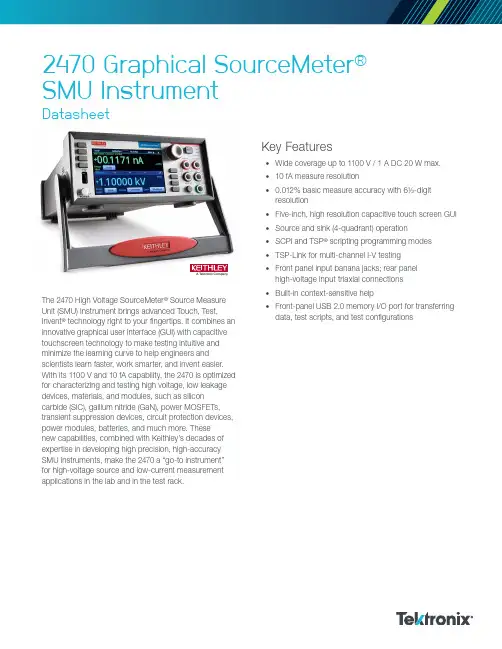
The 2470 High Voltage SourceMeter® Source Measure Unit (SMU) Instrument brings advanced Touch, Test, Invent® technology right to your fingertips. It combines an innovative graphical user interface (GUI) with capacitive touchscreen technology to make testing intuitive and minimize the learning curve to help engineers and scientists learn faster, work smarter, and invent easier. With its 1100 V and 10 fA capability, the 2470 is optimized for characterizing and testing high voltage, low leakage devices, materials, and modules, such as silicon carbide (SiC), gallium nitride (GaN), power MOSFETs, transient suppression devices, circuit protection devices, power modules, batteries, and much more. Thesenew capabilities, combined with Keithley’s decades of expertise in developing high precision, high-accuracy SMU instruments, make the 2470 a “go-to instrument” for high-voltage source and low-current measurement applications in the lab and in the test rack.Key Features• Wide coverage up to 1100 V / 1 A DC 20 W max.• 10 fA measure resolution• 0.012% basic measure accuracy with 6½-digit resolution• Five-inch, high resolution capacitive touch screen GUI • Source and sink (4-quadrant) operation• SCPI and TSP® scripting programming modes• TSP-Link for multi-channel I-V testing• Front panel input banana jacks; rear panelhigh-voltage input triaxial connections• Built-in context-sensitive help• Front-panel USB 2.0 memory I/O port for transferring data, test scripts, and test configurationsDatasheetA Tektronix CompanyDatasheet2Learn Faster; Work Smarter; Invent EasierThe 2470 features a five-inch, full-color, high resolution touchscreen that supports intuitive operation, helps operators become familiar with the instrument quickly, and optimizes overall speed and productivity. A simple icon-based menu structure reduces the number of steps required to configure a test by as much as 50 percent and eliminates the cumbersome multi-layer menu structures typically used on soft-key instruments. Built-in, context-sensitive help supports intuitive operation and minimizes the need to review a separate manual. These capabilities, combined with the 2470’s high versatility, simplify its operation in both basic and advanced measurementapplications, regardless of the user’s previous experience in working with SMU instruments.All-in-One SMU InstrumentThe 2470, Keithley’s fourth generation of SourceMeter SMUs, leverages the proven capabilities of the original 2410 High Voltage SourceMeter SMU Instrument. SMU instruments offer a highly flexible, four-quadrant voltage and current source/load coupled with precision voltage and current measurements. This all-in-one instrument has the capabilities of a:• Precision power supply with V and I readback • True current source• Digital multimeter (DCV, DCI, ohms, and power with 6½-digit resolution)• Precision electronic load • Trigger controller2470 main home screen.2470 icon-based menu.2470 power envelope. 32470 Graphical SourceMeter ® SMU Instrument Data SheetOnline USB 2.0memory I/OFront/rear input selectorRotary navigation/control knobEase of Use Beyond the TouchscreenIn addition to its five-inch color touchscreen, the 2470 front panel offers a variety of features that enhance its speed, user-friendliness, and learnability, including a USB 2.0 memory I/O port, a HELP key, a rotary navigation/control knob, a front/rear input terminal selector button, and banana jacks for basic bench applications. The USB 2.0 memory port simplifies storing test results and instrument configurations, uploading test scripts into the instrument, and installing system upgrades. All front-panel buttons are backlit to enhance visibility in low-light environments. Four Quick Setup modes simplify instrument setup. With one touch, the instrument can be quickly configured for various operating modes without the need to configure the instrument indirectly for this operation.Comprehensive Built-in ConnectivityRear panel access to rear-input connectors, remote control interfaces (GPIB, USB 2.0, and LXI/Ethernet), a D-sub 9-pin digital I/Oport (for internal/external trigger signals and handler control), instrument interlock connector, and TSP-Link ® connectors make it simple to configure multiple instrument test solutions and eliminate the need to invest in additional adapter accessories.2470 front panel with high-resolution, capacitive touchscreen.Rear panel connections are optimized for signal integrity and speed system setup.One-touch Quickset modes speed measurement setups and minimize the time to measurements.EthernetDigital I/O TSP-Link GPIBInterlockUSBDatasheet4Convert Raw Data to InformationA full graphical plotting window converts raw data and displays it immediately as useful information, such as semiconductor I-V curves and waveforms. Using the 2470’s Sheet view, test data can also be displayed in tabular form. The instrument supports exporting data to a spreadsheet for further analysis, dramatically improving productivity for research, benchtop testing, device qualification, and debugging.Built-in data display, charting, and spreadsheet export functions simplify converting test results into useful information.TriggerFlow ® Building Blocks for Instrument Control and ExecutionThe 2470 incorporates Keithley’s TriggerFlow triggering system, which provides user control of instrument execution. TriggerFlow diagrams are created in much the same way that flow charts are developed, using four building blocks:• Wait – Waits for an event to occur before the flow continues • Branch – Branches when a condition has been satisfied• Action – Initiates an action in the instrument, for example, measure, source, delay, set digital I/O, etc.• Notify – Notifies other equipment that an eventhas occurredTriggerFlow building blocks allow creating triggering models that range from very simple to highly complex.A TriggerFlow model using a combination of these building blocks can be created from the front panel or by sending remote commands. With the TriggerFlow system, users can build triggering models from very simple to complex with up to 255 block levels. The 2470 also includes basic triggering functions, including immediate, timer, and manual triggering. 52470 Graphical SourceMeter ® SMU Instrument Data SheetUnmatched System Integration and Programming FlexibilityWhen a 2470 is configured into a multi-channel I-V test system, its embedded Test Script Processor (TSP ®)allows it to run test scripts, so users can create powerful measurement applications with significantly-reduced development times. TSP technology also offers channel expansion without a mainframe. Keithley’s TSP-Link ® channel expansion bus can connect multiple 2470s and other TSP instruments, including Keithley’s other graphical SourceMeter instruments (2450, 2460, 2461), Keithley’s DMM7510, DMM6500, and DAQ6510 graphical multimeters, Series 2600B System SourceMeter SMU instruments, and Series 3700A Switch/Multimeter systems, in a master-subordinate configuration that operates as one integrated system. The TSP-Link expansion bus supports up to 32 units per GPIB or IP address, making it easy to scale a system to fit an application’s particular requirements.Parallel Test CapabilityThe TSP technology in the 2470 supports testing multiple devices in parallel to meet the needs of device research, advanced semiconductor lab applications, and even high throughput production test. This parallel testing capability allows each instrument in the system to run its own complete test sequence, creating a fully multi-threaded test environment. The number of tests that can be run in parallel on a graphical SourceMeter can be as high as the number of instruments in the system.Typical ApplicationsIdeal for current/voltage characterization and functional test of a wide range of today’s modern electronics and devices, including:• Devices–Power semiconductors and materials: SiC, GaN, power MOSFETs, power diodes –IGBT–Thyristors, SCRs–Transient suppression devices –Circuit protection devices: TVS, MOVs, fuses, etc. –Connectors, switches, relays –Power management modules –Batteries • Tests–I-V characterization –Forward voltage –Breakdown voltage –Leakage current –Isolation –Hi-Pot–Dielectric withstandingThe 2470 is the ideal addition to your development bench for designing today’s high power devices and components.Characterize transistors with multiple SMU instruments on wafer or packaged transistorsDatasheet6Instrument Control Start-up SoftwareKickStart instrument control/start-up software enables users to start making measurements in minutes without programming. In most cases, users merely need to make some quick measurements, graph the data, and store the data to disk for later analysis in software environments such as Excel. KickStart offers:• Instrument configuration control to perform I-V characterization • Native X-Y graphing, panning, and zooming • Spreadsheet/tabular viewing of data• Saving and exporting of data for further analysis • Saving of test setups• Screenshot capturing of graphs • Annotating of tests• Command line dialog for sending and receiving data • HTML help• GPIB, USB 2.0, Ethernet complianceSimplified Programming with Ready-to-Use Instrument DriversFor those who prefer to create their own customized application software, native National Instruments LabVIEW ® drivers, and IVI-C and IVICOM drivers are available at /keithley.KickStart start-up software lets users be ready to make measurements in minutes.2470 Graphical SourceMeter® SMU Instrument Data SheetSpecificationsVoltage Specifications1, 2Current Specifications1, 2Notes1. Speed = 1 PLC.2. All specifications are guaranteed with output ON.3. Accuracies apply to 2-wire and 4-wire modes when properly zeroed. For the 200 mV and 1 A ranges, the voltage burden may exceed the specification in 2-wire mode.4. Maximum display and programmming ranges are 5% overrange for voltage, except for the 1000 V range, which is 10% overrange (1100 V), and 5% overrange for current (for example,1.05 A on the 1 A range).5. For sink mode, accuracy is ±(0.15% + offset × 4) except for 1 A range, accuracy is: ± (1.5% + offset × 8).6. Rear-panel triaxial connections only.Resistance Measurement Accuracy (Local Or Remote Sense)7, 8, 97Datasheet8Temperature Coefficient ± (0.15 × accuracy specification)/°C 0 °C to 18 °C and 28 °C to 50 °CSource Current, Measure Resistance ModeTotal uncertainty = I source accuracy + V measure accuracy (4-wire remote sense)Source Voltage, Measure Resistance ModeTotal uncertainty = V source accuracy + I measure accuracy (4-wire remote sense)Guard Output Impedance ≥ 300 Ω typicalNotes7. Speed = 1 PLC.8. All specifications are guaranteed with output ON.9. Accuracies apply to 2-wire and 4-wire modes when properly zeroed.10. Measure resolution 6.5 digits.11. Source readback enabled; offset compensation on.12. Source current, measure resistance or source voltage, measure resistance only.13. Rear-panel triaxial connections only.Supplemental SpecificationsOverrange 105% of range for 200 mV to 200 V, source and measure ranges; 110% of range for 1000 V, source and measure rangesRegulationVoltage Line: 0.01% of rangeLoad: 0.01% of range + 100 µV Current Line: 0.01% of rangeLoad: 0.01% of range + 100 pA Source LimitsVoltage Source Current Limit Bipolar current limit set with a single valueMinimum value is 10% of range Current Source Voltage Limit Bipolar voltage limit set with a single valueMinimum value is 10% of rangeVoltage Limit/Current Limit AccuracyAdd 0.3% of range and ±0.02% of reading to base specification OvershootVoltage Source < 0.1% typicalStep size = Full scale, resistive load, 20 V range, 10 mA current limit Current Source < 0.1% typicalStep size = Full scale, resistive load of 10 kΩ, 1 mA range, 20 V voltage limitRange Change Overshoot Overshoot into a fully resistive 100 kΩ load, 10 Hz to 20 MHz bandwidth, adjacent ranges: 250 mV typical Output Settling Time Time required to reach within 0.1% of final value: 20 V range, 100 mA current limit: < 200 µs typical Maximum Slew Rate 14 0.2 V/µs, 200 V range, 100 mA limit into a 2 kΩ load (typical) 0.5 V/µs, 1000 V range, 10 mA limit into a 100 kΩ load (typical)Overvoltage Protection User-selectable values, 10% tolerance; factory default = none Voltage Source Noise 10 Hz to 20 MHz (RMS): 4 mV typical into a resistive load Common Mode Voltage 250 V DCCommon Mode Isolation> 1 GΩ, < 1000 pFNotes14. High capacitance mode off.2470 Graphical SourceMeter® SMU Instrument Data Sheet Noise Rejection (typical)Load ImpedanceNormal Mode 20 nF typicalHigh-Capacitance Mode Stable into 1 μF typical (specification only valid for ranges ≥100 μA)Maximum Voltage Drop Between Force and Sense Terminals5 VMaximum Sense Lead Resistance 1 MΩ for rated accuracySense Input Impedance > 10 GΩGuard Offset Voltage < 300 µV typicalSystem Measurement Speeds 15Reading rates (readings per second) typical for 60 Hz (50 Hz), script (TSP) programmedReading rates (readings per second) typical for 60 Hz (50 Hz), SCPI programmed16Notes15. Reading rates applicable for voltage or current measurements, autozero off, autorange off, filter off, binary reading format, and source readback off.16. SCPI programming mode.9Datasheet10General Characteristics(Default mode unless specified)Factory Default Standard Power-Up SettingSCPI mode Source Output ModesFixed DC levelMemory/configuration list (mixed function) Stair (linear and logarithmic)Memory Buffer >5,000,000 readings with selected measured values and timestamp Real-Time Clock Lithium battery backup (more than 3 years of battery life)Remote Interfaces GPIB: IEEE Std 488.1 compliant; supports IEEE Std 488.2 common commands and status model topology USB device (rear panel, type B): 2.0 full-speed USBTMCUSB host (front panel, type A): USB 2.0, support for flash drives, FAT32Ethernet: RJ-45 connector, 10/100 BT IP Configuration Static or DHCPExpansion Interface The TSP-Link ® expansion interface allows TSP-enabled instruments to trigger and communicate with each otherLXI Compliance LXI version 1.4 Core 2011TSP Mode Embedded Test Script Processor (TSP) accessible from any host interface DisplayFive-inch capacitive touch, color TFT WVGA (800 × 480) with LED backlight Input Signal Connections Front: Banana. Rear: High-voltage triaxial Programmability SCPI or TSP command sets Interlock Active high-inputDigital I/OLines: Six input/output, user-defined, for digital I/O or triggeringConnector: 9-pin female D Input Signal Levels: 0.7 V (maximum logic low), 3.7 V (minimum logic high) Input Voltage Limits: –0.25 V (absolute minimum), +5.25 V (absolute maximum) Maximum Source Current: +2.0 mA at > 2.7 V (per pin)Maximum Sink Current: –50 mA at 0.7 V (per pin, solid-state fuse protected)5 V Power Supply Pin: Limited to 500 mA at > 4 V (solid-state fuse protected)Handler: User-definable start of test, end of test, four category bits CoolingForced air, variable speedOvertemperature Protection Internally sensed temperature overload puts instrument in standby mode Power Supply 100 VRMS to 240 VRMS, 50 Hz or 60 Hz (automatically detected at power up)VA Rating 220 VA maximumAltitude Maximum 2000 meters (6562 feet) above sea level EMC Conforms to European Union EMC DirectiveSafety NRTL listed to UL61010-1 and UL61010-2-30; conforms to European Union Low Voltage Directive RoHS Conforms to European Union Restriction on Hazardous Substances Directive Vibration MIL -PRF-28800F Class 3 Random Warm upOne hour to rated accuracies2470 Graphical SourceMeter® SMU Instrument Data SheetDimensions With handle and bumpers: 106 mm × 255 mm × 425 mm (4.18 in. high × 10.05 in. wide × 16.75 in. deep)Without handle and bumpers: 88 mm × 213 mm × 403 mm (3.46 in. high × 8.39 in. wide × 15.87 in. deep) Weight With handle and bumpers: 4.54 kg (10 lb)Without handle and bumpers: 4.08 kg (9.0 lb)Environment Operating: 0 °C to 50 °C, 70% relative humidity up to 35 °C; derate 3% relative humidity/°C, 35 °C to 50 °C Storage: –25 °C to 65 °CPollution Category: 2SourceMeter® is a registered trademark of Keithley Instruments LLC. All other trademarks are the property of their respective owners. Supplied Accessories8608 High Performance Test LeadsUSB-B-1 USB Cable, Type A to Type B, 1 m (3.3 ft)CS-1616-3 Safety Interlock Mating Connector17469460X TSP-Link/Ethernet Cable2470 QuickStart GuideTest Script Builder Software (available at )LabVIEW and IVI Drivers (available at )Available AccessoriesTest Leads and Probes8605 High Performance Modular Test Leads8606 High Performance Modular Probe Kit8608 High Performance Test LeadsCables, Connectors, AdaptersTRX-1100V-BAN HV Triax to Banana Adapter. Converts the 4 triax connectors on the rear panel to 5 banana jacksTRX-1100V-* 3-slot HV Low Noise Triax Cable (0.5 m, 1 m, 2 m, 3 m lengths available)8607 2-wire, 1000 V Banana Cables, 1 m (3.3 ft)CS-1616-3 Safety Interlock Mating ConnectorCommunication Interfaces & Cables7007-1 Shielded GPIB Cable, 1 m (3.3 ft)7007-2 Shielded GPIB Cable, 2 m (6.6 ft)17469460X TSP-Link Ethernet CableKPCI-488LPA IEEE-488 Interface for PCI BusKUSB-488B IEEE-488 USB-to-GPIB Interface AdapterUSB-B-1 USB Cable, Type A to Type B, 1 m (3.3 ft)11Datasheet12Triggering and Control2450-TLINK DB-9 to Trigger Link Connector Adapter 8501-1 Trigger Link Cable, DIN-to-DIN, 1 m (3.3 ft.)8501-2Trigger Link Cable, DIN-to-DIN, 2 m (6.6 ft.)Rack Mount Kits4299-8 Single Fixed Rack Mount Kit 4299-9 Dual Fixed Rack Mount Kit4299-10 Dual Fixed Rack Mount Kit. Mount one 2450 and one Series 26xxB4299-11Dual Fixed Rack Mount Kit. Mount one 2450 and one Series 2400, Series 2000, etc.Available Services2470-3Y-EW 1-year factory warranty extended to 3 years from date of shipment 2470-5Y-EW 1-year factory warranty extended to 5 years from date of shipment C/2470-3Y-17025 KeithleyCare ® 3 Year ISO 17025 Calibration Plan C/2470-3Y-DATA KeithleyCare 3 Year Calibration w/Data Plan C/2470-3Y-STD KeithleyCare 3 Year STD Calibration Plan C/2470-5Y-17025 KeithleyCare 5 Year ISO 17025 Calibration Plan C/2470-5Y-DATA KeithleyCare 5 Year Calibration w/Data Plan C/2470-5Y-STD KeithleyCare 5 Year STD Calibration Plan C/NEW DATA Calibration Data for New UnitsC/NEW DATA ISOISO-17025 Calibration Data for New UnitsOrdering Information24701000 V, 1 A, 20 W SourceMeter SMU InstrumentWarranty InformationWarranty SummaryThis section summarizes the warranties of the 2470. For complete warranty information, refer to theTektronix warranty page at https:///service/warranties/warranty-2. Any portion of the product that is not manufactured by Keithley is not covered by this warranty and Keithley will have no duty to enforce any other manufacturer’s warranties.Hardware WarrantyKeithley warrants the Keithley manufactured portion of the hardware for a period of one year from defects in materials or workmanship; provided that such defect has not been caused by use of the Keithleyhardware which is not in accordance with the hardware instructions. The warranty does not apply upon any modification of Keithley hardware made by the customer or operation of the hardware outside the environmental specifications.Software WarrantyKeithley warrants for the Keithley produced portion of the software or firmware will conform in all material respects with the published specifications for a period of ninety (90) days; provided the software is used on the product for which it is intended in accordance with the software instructions. Keithley does not warrant that operation of the software will be uninterrupted or error-free, or that the software will be adequate for the customer’s intended application. The warranty does not apply upon any modification of the software made by the customer.2470 Graphical SourceMeter® SMU Instrument Data Sheet13Contact Information:Australia* 1 800 709 465Austria 00800 2255 4835Balkans, Israel, South Africa and other ISE Countries +41 52 675 3777Belgium* 00800 2255 4835Brazil +55 (11) 3759 7627Canada 180****9200Central East Europe / Baltics +41 52 675 3777Central Europe / Greece +41 52 675 3777Denmark +45 80 88 1401Finland +41 52 675 3777France* 00800 2255 4835Germany* 00800 2255 4835Hong Kong 400 820 5835India 000 800 650 1835Indonesia 007 803 601 5249Italy 00800 2255 4835Japan 81 (3) 6714 3010Luxembourg +41 52 675 3777Malaysia 180****5835Mexico, Central/South America and Caribbean 52 (55) 56 04 50 90Middle East, Asia, and North Africa +41 52 675 3777The Netherlands* 00800 2255 4835New Zealand 0800 800 238Norway 800 16098People’s Republic of China 400 820 5835Philippines 1 800 1601 0077Poland +41 52 675 3777Portugal 80 08 12370Republic of Korea +82 2 565 1455Russia / CIS +7 (495) 6647564Singapore 800 6011 473South Africa +41 52 675 3777Spain* 00800 2255 4835Sweden* 00800 2255 4835Switzerland* 00800 2255 4835Taiwan 886 (2) 2656 6688Thailand 1 800 011 931United Kingdom / Ireland* 00800 2255 4835USA 180****9200Vietnam 12060128* European toll-free number. If notaccessible, call: +41 52 675 3777Find more valuable resources at Copyright © Tektronix. All rights reserved. Tektronix products are covered by U.S. and foreign patents, issued and pending. Information in this publication supersedes thatin all previously published material. Specification and price change privileges reserved. TEKTRONIX and TEK are registered trademarks of Tektronix, Inc. All other trade namesreferenced are the service marks, trademarks or registered trademarks of their respective companies.060719.SBG 1KW-61523-0。
SPS-8340WG中文资料
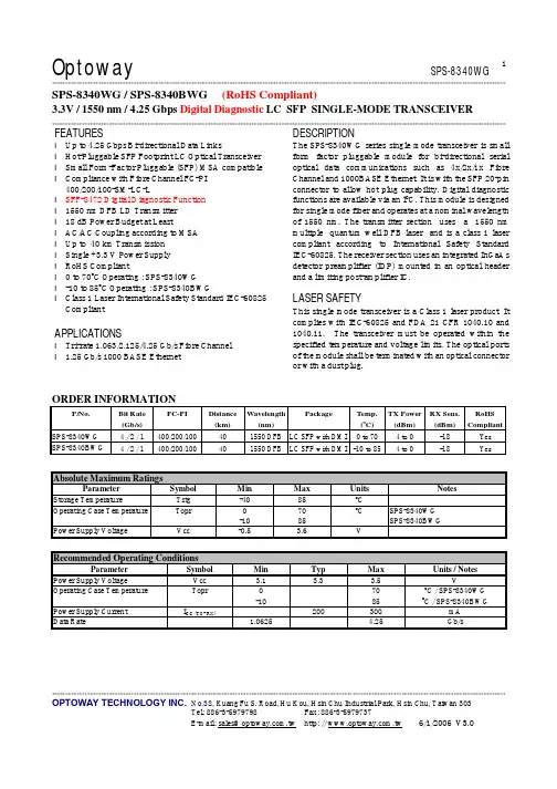
Optoway SPS-8340WG********************************************************************************************************************************************************************************************************************************************************************************************************************************************OPTOWAY TECHNOLOGY INC. No .38, Kuang Fu S. Road, Hu Kou, Hsin Chu Industrial Park, Hsin Chu, Taiwan 303Tel: 886-3-5979798 Fax: 886-3-59797371SPS-8340WG / SPS-8340BWG (RoHS Compliant)3.3V / 1550 nm /4.25 Gbps Digital Diagnostic LC SFP SINGLE-MODE TRANSCEIVER **********************************************************************************************************************************************************************FEATURESl Up to 4.25 Gbps Bi-directional Data Linksl Hot-Pluggable SFP Footprint LC Optical Transceiver l Small Form-Factor Pluggable (SFP) MSA compatible l Compliance with Fibre Channel FC-PI 400/200/100-SM-LC-Ll SFF-8472 Digital Diagnostic Function l 1550 nm DFB LD Transmitter l 18 dB Power Budget at Leastl AC/AC Coupling according to MSA l Up to 40 km Transmission l Single +3.3 V Power Supply l RoHS Compliantl 0 to 70o C Operating : SPS-8340WG l -10 to 85o C Operating : SPS-8340BWGl Class 1 Laser International Safety Standard IEC-60825 CompliantAPPLICATIONSl Tri-rate 1.063/2.125/4.25 Gb/s Fibre Channel l 1.25 Gb/s 1000 BASE EthernetDESCRIPTIONThe SPS-8340WG series single mode transceiver is small form factor pluggable module for bi-directional serial optical data communications such as 4x/2x/1x Fibre Channel and 1000BASE Ethernet. It is with the SFP 20-pin connector to allow hot plug capability. Digital diagnostic functions are available via an I 2C. This module is designed for single mode fiber and operates at a nominal wavelength of 1550 nm. The transmitter section uses a 1550 nm multiple quantum well DFB laser and is a class 1 laser compliant according to International Safety Standard IEC-60825. The receiver section uses an integrated InGaAs detector preamplifier (IDP) mounted in an optical header and a limiting post-amplifier IC.LASER SAFETYThis single mode transceiver is a Class 1 laser product. It complies with IEC-60825 and FDA 21 CFR 1040.10 and 1040.11. The transceiver must be operated within the specified temperature and voltage limits. The optical ports of the module shall be terminated with an optical connector or with a dust plug.ORDER INFORMATIONP/No.Bit Rate (Gb/s) FC-PI Distance (km) Wavelength(nm)PackageTemp. (o C) TX Power (dBm) RX Sens. (dBm) RoHS Compliant SPS-8340WG4 / 2 / 1 400/200/100 40 1550 DFB LC SFP with DMI0 to 704 to 0 -18 Yes SPS-8340BWG4 / 2 / 1400/200/100401550 DFB LC SFP with DMI -10 to 854 to 0-18YesAbsolute Maximum RatingsParameterSymbol Min Max Units NotesStorage TemperatureTstg -40 85 o COperating Case Temperature Topr 0 -10 70 85 o C SPS-8340WG SPS-8340BWG Power Supply VoltageVcc-0.53.6VRecommended Operating ConditionsParameterSymbol Min Typ Max Units / NotesPower Supply VoltageVcc 3.1 3.3 3.5 VOperating Case Temperature Topr 0 -10 70 85 oC / SPS-8340WG oC / SPS-8340BWGPower Supply Current I CC (TX+RX)200 300 mA Data Rate1.06254.25Gb/s*******************************************************************************************************************************************************************************OPTOWAY TECHNOLOGY INC. No .38, Kuang Fu S. Road, Hu Kou, Hsin Chu Industrial Park, Hsin Chu, Taiwan 303Transmitter Specifications (0o C < Topr < 70o C, 3.1V < Vcc < 3.5V)ParameterSymbolMinTypMaxUnits Notes OpticalOptical Transmit Power Po 0 --- 4 dBm 1 Optical Modulation Amplitude@4.25Gb/s OMA 1200 --- µWOutput Center Wavelength λ 1480 1580 nmOutput Spectrum Width ∆λ --- 1 nm -20 dB Width Side Mode Suppression Ratio SMSR 30 dBOptical Rise / Fall Time t r /t f 90 ps 20 % to 80%,unfiltered Relative Intensity Noise RIN -120 dB/HzElectricalData Input Current – Low I IL -350 µA Data Input Current – High I IH 350 µADifferential Input Voltage V IH - V IL 0.5 2.4 V Peak-to-PeakTX Disable Input Voltage – Low T DIS, L 0 0.5 V 2 TX Disable Input Voltage – High T DIS, H 2.0 Vcc V 2 TX Disable Assert Time T ASSERT 10 µs TX Disable Deassert Time T DEASSERT 1 ms TX Fault Output Voltage -- Low T FaultL 0 0.5 V 3 TX Fault Output Voltage -- High T FaultH 2.0 Vcc+0.3 V31. Output power is power coupled into a 9/125 µm single mode fiber.2. There is an internal 4.7K to 10K ohm pull-up resistor to VccTX.3. Open collector compatible,4.7K to 10K ohm pull-up to Vcc (Host Supply Voltage).Receiver Specifications (0o C < Topr < 70o C, 3.1V < Vcc < 3.5V)ParameterSymbol Min Typ Max Units NotesOpticalSensitivity @4.25Gb/s Sens1 29 -18 µW dBm 4 5 Sensitivity @2.125 / 1.063Gb/sSens215 -20 µW dBm 4 5 Maximum Input Power Pin 0 dBmSignal Detect -- Asserted Pa --- -18 dBm Transition: low to high Signal Detect -- Deasserted Pd -30 --- --- dBm Transition: high to low Signal detect -- Hysteresis 1.0 --- dBWavelength of Operation 1260 --- 1600nmElectricalDifferential Output Voltage V OH – V OL 0.6 2.0 V Output LOS Voltage -- Low V OL 0 0.5 V 6 Output LOS Voltage -- High V OH 2.0 Vcc+0.3 V 64. Measured at PRBS 2-1 at BER 1E-12.5. Represents sensitivity based on OMA spec, as corrected to incoming Extinction Ratio of 9 dB. For example, an OMA of 29 µW is approximately equal to an average power of -17.3 dBm, average with an Extinction ratio of 9 dB.6. Open collector compatible, 4.7K to 10K ohm pull-up to Vcc (Host Supply Voltage).*******************************************************************************************************************************************************************************OPTOWAY TECHNOLOGY INC. No .38, Kuang Fu S. Road, Hu Kou, Hsin Chu Industrial Park, Hsin Chu, Taiwan 303PINSignal NameDescriptionPINSignal Name Description1 TX GND Transmitter Ground11 RX GND Receiver Ground2 TX Fault Transmitter Fault Indication12 RX DATA OUT- Inverse Receiver Data Out 3 TX Disable Transmitter Disable (Module disables on high or open)13 RX DATA OUT+ Receiver Data Out 4 MOD-DFE2 Modulation Definition 2 – Two wires serial ID Interface14 RX GND Receiver Ground5 MOD-DEF1 Modulation Definition 1 – Two wires serial ID Interface15 Vcc RX Receiver Power – 3.3V ±5% 6 MOD-DEF0 Modulation Definition 0 – Ground in Module16 Vcc TX Transmitter Power – 3.3V ±5% 7 N/C Not Connected 17 TX GNDTransmitter Ground 8 LOS Loss of Signal 18 TX DATA IN+ Transmitter Data In9 RX GND Receiver Ground 19 TX DATA IN- Inverse Transmitter Data In 10RX GNDReceiver Ground20TX GNDTransmitter GroundModule DefinitionModule DefinitionMOD-DEF2 PIN 4 MOD-DEF1 PIN 5 MOD-DEF0 PIN 6 Interpretation by Host 4SDASCLLV-TTL LowSerial module definitionprotocolModule Definition 4 specifies a serial definition protocol. For this definition, upon power up, MOD-DEF(1:2) appear as no connector (NC) and MOD-DEF(0) is TTL LOW. When the host system detects this condition, it activates the serial protocol. The protocol uses the 2-wire serial CMOS E 2PROM protocol of the ATMEL AT24C01A/02/04 family of components.No.38, Kuang Fu S. Road, Hu Kou, Hsin Chu Industrial Park, Hsin Chu, Taiwan 303。
KSZ8993M,KSZ8993M,KS8993M,KS8993MI,KS8993ML, 规格书,Datasheet 资料
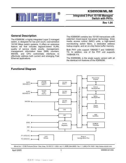
KS8993M/ML/MIIntegrated 3-Port 10/100 ManagedSwitch with PHYsRev 1.04 Micrel Inc. • 2180 Fortune Drive • San Jose, CA 95131 • USA • tel +1 (408) 944-0800 • fax + 1 (408) 474-1000 • General DescriptionThe KS8993M, a highly integrated Layer 2 managedswitch, is designed for low port count, cost-sensitive10/100 Mbps switch systems. It offers an extensivefeature set that includes tag/port-based VLAN,quality of service (QoS) priority, management,management information base (MIB) counters,MII/SNI, and CPU control/data interfaces toeffectively address both current and emerging FastEthernet applications.The KS8993M contains two 10/100 transceivers withpatented mixed-signal low-power technology, threemedia access control (MAC) units, a high-speednon-blocking switch fabric, a dedicated addresslookup engine, and an on-chip frame buffer memory.Both PHY units support 10BASE-T and 100BASE-TX. In addition, one of the PHY unit supports100BASE-FX.The KS8993ML is the single supply version with allthe identical rich features of the KS8993M.___________________________________________________________________________________________________ Functional DiagramAUT OAUT OMDI/MDI-XMII/SNISPIMIIMSMII2CP1 LED[3:0]P2 LED[3:0]Features• Proven Integrated3-Port 10/100 Ethernet Switch – 2nd generation switch with three MACs and two PHYs fully compliant to IEEE 802.3u standard– Non-blocking switch fabric assures fast packetdelivery by utilizing a 1K MAC address lookup table and a store-and-forward architecture– Full duplex IEEE 802.3x flow control (pause) with force mode option– Half-duplex back pressure flow control– Automatic MDI/MDI-X crossover with disable and enable option– 100BASE-FX support on port 1– MII interface supports both MAC mode and PHY mode– 7-wire serial network interface (SNI) support forlegacy MAC– Comprehensive LED Indicator support for link,activity, full/half duplex and 10/100 speed• Comprehensive Configuration Register Access – Serial management interface (SMI) to all internal registers– MII management (MIIM) interface to PHY registers – SPI and I2C Interface to all internal registers– I/0 Pins strapping and EEPROM to programselective registers in unmanaged switch mode– Control registers configurable on the fly (port-priority, 802.1p/d/q, AN…)• QoS/CoS Packet Prioritization Support– Per port, 802.1p and DiffServ-based– Re-mapping of 802.1p priority field per port basis • Advanced Switch Features– IEEE 802.1q VLAN support for up to 16 groups(full-range of VLAN ID)– VLAN ID tag/untag options, per port basis– IEEE 802.1p/q tag insertion or removal on a perport basis (egress)– Programmable rate limiting from 0Mbps to100Mbps at the ingress and egress port, rate options for high and low priority per port basis– Broadcast storm protection with % control (global and per port basis)– IEEE 802.1d spanning tree protocol support– Upstream special tagging mode to inform the processor which ingress port receives the packet– IGMP v1/v2 snooping support for multicast packet filtering– Double-tagging support • Switch Management Features– Port mirroring/monitoring/sniffing: ingress and/or egress traffic to any port or MII– MIB counters for fully compliant statisticsgathering, 34 MIB counters per port– Loopback modes for remote diagnostic of failure • Low Power Dissipation: <0.8 Watts (includes PHY transmit drivers)– Full-chip hardware power-down (registerconfiguration not saved)– Per port based software power-save on PHY (idle link detection, register configuration preserved)– 0.18um CMOS technology– Voltages: Core 1.8VI/O and Transceiver 3.3VUse K8993ML for 3.3V only operation • Industrial Temperature Range: –40o C to +85o C• Available in128-Pin PQFPApplications• Universal Solutions– Broadband gateway / Firewall / VPN– Integrated DSL or cable modem multi-port router – Wireless LAN access point + gateway– Residential and enterprise VoIP gateway/phone – Set-top/game box– Home networking expansion– Standalone 10/100 switch– FTTx customer premises equipment– Fiber broadband gateway• Upgradeable Solutions(1)– Unmanaged switch with future option to migrate toa managed solution– Single PHY alternative with future expansionoption for two ports• Industrial Solutions– Applications requiring port redundancy and port monitoring– Sensor devices in redundant ring topologyNote:1. The cost and time of PCB re-spin.Ordering InformationPart Number Temperature Range PackageKS8993M 0o C to 70o C128-Pin PQFPKS8993ML 0o C to 70o C128-Pin PQFPKS8993MI –40o C to +85o C128-Pin PQFPKSZ8993M 0o C to 70o C128-Pin PQFP, Lead-free KSZ8993ML 0o C to 70o C 128-Pin PQFP, Lead-freeRevision HistoryRevision Date Summary of ChangesCreated.1.00 5/14/031.01 5/28/03 Added KS8993MI availability in Q4 2003.1.02 12/8/03Changed V DDIO, V DDATX and V DDARX supply voltagesfrom 3.3V to (3.3V or 2.5V).Changed [PS1,PS0] = [1,1] setting from Reserved to SMI mode.Changed Special Tagging Mode to Upstream Special Tagging Mode(Switch port 3 to processor support only).Updated recommended magnetic manufacturer list.Added 25MHz crystal/oscillator clock’s ppm spec. in Pin Description.Updated I2C Slave Serial Bus Configuration section.Updated KS8993MI availability to from Q1 2004.1.03 9/22/04Added KS8993ML to General Description (page 1) and to the FunctionalDescription.Updated Part Ordering Information table.Updated pin description for pin 22 to the following:V DDC: For KS8993M, this is an input power pin for the 1.8V digitalV DD.coreV OUT_1V8: For KS8993ML, this is an 1.8V output power pin tosupply the KS8993ML’s input power pins: V DDAP(pin 63), V DDC (pins 91, 123), and V DDA (pins 38,43, 57).Updated pin description for P1LED3 (pin 25) to indicate that an external1K pull-down is needed if a LED is connected.Updated pin description for MDIO (pin 95) to indicate that an external4.7K pull-up is needed if this pin is in used.Changed the aging period from 300 +/–75 seconds to about 200 seconds.Updated Electrical Characteristics (V IH, V IL, V OH, V OL).Transferred to new format.1.04 4/12/05Removed references to 2.5V operationAdded reset circuit recommendationContentsList of Figures (8)List of Tables (8)Pin Description and I/O Assignment (9)Pin Configuration (19)Functional Description (20)Functional Overview: Physical Layer Transceiver (20)100BASE-TX Transmit (20)100BASE-TX Receive (20)PLL Clock Synthesizer (21)Scrambler/De-scrambler (100BASE-TX Only) (21)100BASE-FX Operation (21)100BASE-FX Signal Detection (21)100BASE-FX Far End Fault (21)10BASE-T Transmit (21)10BASE-T Receive (22)Power Management (22)MDI /MDI-X Auto Crossover (22)Straight Cable (23)Crossover Cable (24)Auto Negotiation (24)Functional Overview: MAC and Switch (26)Address Lookup (26)Learning (26)Migration (26)Aging (26)Forwarding (26)Switching Engine (29)MAC Operation (29)Inter Packet Gap (IPG) (29)Back-Off Algorithm (29)Late Collision (29)Illegal Frames (29)Flow Control (29)Half-Duplex Backpressure (29)Broadcast Storm Protection (30)MII Interface Operation (30)SNI (7-Wire) Operation (31)MII Management Interface (MIIM) (31)Serial Management Interface (SMI) (32)Advanced Switch Functions (33)Spanning Tree Support (33)Upstream Special Tagging Mode (34)IGMP Support (35)“IGMP” Snooping (35)“Multicast Address Insertion” in the Static MAC Table (35)Port Mirroring Support (35)IEEE 802.1Q VLAN Support (35)QoS Priority Support (36)Rate Limiting Support (38)Configuration Interface (38)I2C Master Serial Bus Configuration (38)I2C Slave Serial Bus Configuration (39)SPI Slave Serial Bus Configuration (39)Loopback Support (43)MII Management (MIIM) Registers (44)Register 0: MII Basic Control (45)Register 2: PHYID HIGH (45)Register 3: PHYID LOW (45)Register 4: Auto-Negotiation Advertisement Ability (46)Register 5: Auto-Negotiation Link Partner Ability (46)Register Map: Switch & PHY (8 bit registers) (47)Global Registers (47)Port Registers (47)Advanced Control Registers (47)Global Registers (47)Register 0 (0x00): Chip ID0 (47)Register 1 (0x01): Chip ID1 / Start Switch (48)Register 2 (0x02): Global Control 0 (48)Register 3 (0x03): Global Control 1 (49)Register 4 (0x04): Global Control 2 (49)Register 5 (0x05): Global Control 3 (50)Register 6 (0x06): Global Control 4 (51)Register 7 (0x07): Global Control 5 (52)Register 8 (0x08): Global Control 6 (52)Register 9 (0x09): Global Control 7 (52)Register 10 (0x0A): Global Control 8 (52)Register 11 (0x0B): Global Control 9 (52)Register 12 (0x0C): Reserved Register (53)Register 13 (0x0D): User Defined Register 1 (53)Register 14 (0x0E): User Defined Register 2 (53)Register 15 (0x0F): User Defined Register 3 (53)Port Registers (54)Register 16 (0x10): Port 1 Control 0 (54)Register 32 (0x20): Port 2 Control 0 (54)Register 48 (0x30): Port 3 Control 0 (54)Register 17 (0x11): Port 1 Control 1 (55)Register 33 (0x21): Port 2 Control 1 (55)Register 49 (0x31): Port 3 Control 1 (55)Register 18 (0x12): Port 1 Control 2 (56)Register 34 (0x22): Port 2 Control 2 (56)Register 50 (0x32): Port 3 Control 2 (56)Register 19 (0x13): Port 1 Control 3 (56)Register 35 (0x23): Port 2 Control 3 (56)Register 51 (0x33): Port 3 Control 3 (56)Register 20 (0x14): Port 1 Control 4 (57)Register 36 (0x24): Port 2 Control 4 (57)Register 52 (0x34): Port 3 Control 4 (57)Register 21 (0x15): Port 1 Control 5 (57)Register 37 (0x25): Port 2 Control 5 (57)Register 53 (0x35): Port 3 Control 5 (57)Register 22 (0x16): Port 1 Control 6 (57)Register 38 (0x26): Port 2 Control 6 (57)Register 54 (0x36): Port 3 Control 6 (57)Register 23 (0x17): Port 1 Control 7 (57)Register 39 (0x27): Port 2 Control 7 (57)Register 55 (0x37): Port 3 Control 7 (57)Register 24 (0x18): Port 1 Control 8 (57)Register 40 (0x28): Port 2 Control 8 (57)Register 56 (0x38): Port 3 Control 8 (57)Register 25 (0x19): Port 1 Control 9 (58)Register 41 (0x29): Port 2 Control 9 (58)Register 57 (0x39): Port 3 Control 9 (58)Register 26 (0x1A): Port 1 Control 10 (58)Register 42 (0x2A): Port 2 Control 10 (58)Register 58 (0x3A): Port 3 Control 10 (58)Register 27 (0x1B): Port 1 Control 11 (58)Register 43 (0x2B): Port 2 Control 11 (58)Register 28 (0x1C): Port 1 Control 12 (59)Register 44 (0x2C): Port 2 Control 12 (59)Register 60 (0x3C): Reserved, not applied to port 3 (59)Register 29 (0x1D): Port 1 Control 13 (60)Register 45 (0x2D): Port 2 Control 13 (60)Register 61 (0x3D): Reserved, not applied to port 3 (60)Register 30 (0x1E): Port 1 Status 0 (61)Register 46 (0x2E): Port 2 Status 0 (61)Register 62 (0x3E): Reserved, not applied to port 3 (61)Register 31 (0x1F): Port 1 Status 1 (62)Register 47 (0x2F): Port 2 Status 1 (62)Register 63 (0x3F): Port 3 Status 1 (62)Advanced Control Registers (63)Register 96 (0x60): TOS Priority Control Register 0 (63)Register 97 (0x61): TOS Priority Control Register 1 (63)Register 98 (0x62): TOS Priority Control Register 2 (63)Register 99 (0x63): TOS Priority Control Register 3 (63)Register 100 (0x64): TOS Priority Control Register 4 (63)Register 101 (0x65): TOS Priority Control Register 5 (63)Register 102 (0x66): TOS Priority Control Register 6 (63)Register 103 (0x67): TOS Priority Control Register 7 (63)Register 104 (0x68): MAC Address Register 0 (64)Register 105 (0x69): MAC Address Register 1 (64)Register 106 (0x6A): MAC Address Register 2 (64)Register 107 (0x6B): MAC Address Register 3 (64)Register 108 (0x6C): MAC Address Register 4 (64)Register 109 (0X6D): MAC Address Register 5 (64)Register 110 (0x6E): Indirect Access Control 0 (65)Register 111 (0x6F): Indirect Access Control 1 (65)Register 112 (0x70): Indirect Data Register 8 (65)Register 113 (0x71): Indirect Data Register 7 (65)Register 114 (0x72): Indirect Data Register 6 (65)Register 115 (0x73): Indirect Data Register 5 (65)Register 116 (0x74): Indirect Data Register 4 (65)Register 117 (0x75): Indirect Data Register 3 (66)Register 118 (0x76): Indirect Data Register 2 (66)Register 119 (0x77): Indirect Data Register 1 (66)Register 120 (0x78): Indirect Data Register 0 (66)Registers 121 to 127 (66)Static MAC Address Table (66)VLAN Table (67)Dynamic MAC Address Table (68)MIB (Management Information Base) Counters (69)Additional Information (72)Absolute Maximum Ratings (73)Operating Ratings (73)Electrical Characteristics (74)Timing Specifications (76)EEPROM Timing (76)SNI Timing (77)MII Timing (77)MAC Mode MII Timing (78)PHY-Mode MII Timing (79)SPI Timing (77)Input Timing (80)Output Timing (81)Reset Timing (82)Selection of Isolation Transformers (84)Selection of Reference Crystal (84)Package Information (85)List of FiguresFigure 1. Typical Straight Cable Connection (24)Figure 2. Typical Crossover Cable Connection (24)Figure 3. Auto Negotiation and Parallel Operation (25)Figure 4. Destination Address Lookup Flow Chart, Stage 1 (27)Figure 5. Destination Address Resolution Flow Chart, Stage 2 (28)Figure 6. 802.1p Priority Field Format (37)Figure 7. KS8993M EEPROM Configuration Timing Diagram (38)Figure 8. SPI Write Data Cycle (41)Figure 9. SPI Read Data Cycle (41)Figure 10. SPI Multiple Write (41)Figure 11. SPI Multiple Read (42)Figure 12. Loopback Path (43)Figure 13. EEPROM Interface Input Timing Diagram (76)Figure 14. EEPROM Interface Output Timing Diagram (76)Figure 15. SNI Input Timing Diagram (77)Figure 16. SNI Output Timing Diagram (77)Figure 17. MAC-Mode MII Timing – Data Received from MII (78)Figure 18. MAC-Mode MII Timing – Data Input to MII (78)Figure 19. PHY-Mode MII Timing – Data Received from MII (79)Figure 20. PHY-Mode MII Timing – Data Input to MII (79)Figure 21. SPI Input Timing (80)Figure 22. SPI Output Timing (81)Figure 23. Reset Timing (82)128-Pin PQFP Package (85)List of TablesTable 1. FX and TX Mode Selection (21)Table 2. MDI/MDI-X Pin Definitions (22)Table 3. MII Signals (30)Table 4. SNI Signals (31)Table 5. MII Management Interface Frame Format (32)Table 6. Serial Management Interface (SMI) Frame Format (32)Table 7. Upstream Special Tagging Mode Format (34)Table 8. STPID Egress Rules (Switch Port 3 to Processor) (34)Table 9. FID+DA Lookup in VLAN Mode (36)Table 10. FID+SA Lookup in VLAN Mode (36)Table 11. KS8993M SPI Connections (40)Table 12. Format of Static MAC Table (8 Entries) (66)Table 13. Format of Static VLAN Table (16 Entries) (68)Table 14. Format of Dynamic MAC Address Table (1K Entries) (68)Table 15. Format of “Per Port” MIB Counters (69)Table 16. Port 1s “Per Port” MIB Counters Indirect Memory Offsets (70)Table 17. Port 1’s “Per Port” MIB Counters Indirect Memory Offsets (71)Table 18. Format of “All Port Dropped Packet” MIB Counters (71)Table 19. “All Port Dropped Packet” MIB Counters Indirect Memory Offsets (71)Table 20. EEPROM Timing Parameters (76)Table 21. SNI Timing Parameters (77)Table 22. MAC-Mode MII Timing Parameters (78)Table 23. PHY-Mode MII Timing Parameters (79)Table 24. SPI Input Timing Parameters (80)Table 25. SPI Output Timing Parameters (81)Table 26. Reset Timing Parameters (82)Table 27. Transformer Selection Criteria (84)Table 28. Qualified Single Port Magnetics (84)Table 29. Typical Reference Crystal Characteristics (84)Pin Description and I/O AssignmentNote:1. Ipu/O = Input with internal pull-up during reset, output pin otherwise.Gnd = Ground.Pin Number Pin Name Type (1) Description 8VDDIOP3.3V digital V DD9 NC Ipd No connect 10 NC Ipd No connect 11 NC Ipu No connect12 ADVFC Ipu1 = advertise the switch’s flow control capability via auto negotiation.0 = will not advertise the switch’s flow control capability via auto negotiation.13 P2ANEN Ipu 1 = enable auto negotiation on port 2 0 = disable auto negotiation on port 2 14P2SPDIpd1 = force port2 to 100BT if P2ANEN = 0 0 = force port 2 to 10BT if P2ANEN = 015 P2DPX Ipd1 = port2 default to full duplex mode if P2ANEN = 1 and auto negotiation fails. Force port 2 in full duplex mode if P2ANEN = 0.0 = port 2 default to half duplex mode if P2ANEN = 1 and auto negotiation fails. Force port 2 in half duplex mode if P2ANEN = 0.16P2FFCIpd1 = always enable (force) port2 flow control feature 0 = port 2 flow control feature enable is determined by auto negotiation result.17 NC Opu No connect 18 NC Ipd No connect 19 NC Ipd No connect 20P2LED3OpdPort 2 LED indicatorNote: Internal pull-down is weak; it will not turn ON the LED.See description in pin 4.21 DGND Gnd Digital ground 22VDDC/VOUT_1V8PV DDC : For KS8993M, this is an input power pin for the 1.8V digital core V DD .V OUT_1V8: For KS8993ML, this is a 1.8V output power pin to supply the KS8993ML’s input power pins: V DDAP (pin 63), V DDC (pins 91 and 123), and V DDA (pins 38, 43, and 57).23LEDSEL1IpdLED display mode select See description in pins 1 and 4.24 NC O No connect 25P1LED3OpdPort 1 LED indicatorNote: An external 1K pull-down is needed on this pin if it isconnected to a LED. The 1K resistor will not turn ON the LED.See description in pin 1.Note:1. P = Power supply. Gnd = Ground. O = Output.Ipu = Input w/ internal pull-up. Ipd = Input w/ internal pull-down. Opu = Output with internal pull-up.Opd = Output internal pull-down.Pin Number Pin Name Type (1) Descriptionconnect26 NC O No27 HWPOVR Ipd Hardware pin overwrite0 = Disable. All strap-in pins configurations are overwritten bythe EEPROM configuration data1 = Enable. All strap-in pins configurations are overwritten bythe EEPROM configuration data, except for register 0x2C bits[7:5], (port 2: auto-negotiation enable, force speed, forceduplex).28 P2MDIXDIS Ipd Port 2 Auto MDI/MDI-XPD (default) = enablePU = disable29 P2MDIX Ipd Port 2 MDI/MDI-X setting when auto MDI/MDI-X is disabled.PD (default) = MDI-X (transmit on TXP2 / TXM2 pins)PU = MDI, (transmit on RXP2 / RXM2 pins)30 P1ANEN Ipu 1 = enable auto negotiation on port 10 = disable auto negotiation on port 131 P1SPD Ipd 1 = force port 1 to 100BT if P1ANEN = 00 = force port 1 to 10BT if P1ANEN = 01 = port 1 default to full duplex mode if P1ANEN = 1 and autoIpd32 P1DPXnegotiation fails. Force port 1 in full-duplex mode if P1ANEN= 0.0 = port 1 default to half duplex mode if P1ANEN = 1 and autonegotiation fails. Force port 1 in half duplex mode if P1ANEN= 0.33 P1FFC Ipd 1 = always enable (force) port 1 flow control feature0 = port 1 flow control feature enable is determined by autonegotiation result.connectNo34 NC Ipd35 NC Ipd No connect36 PWRDN Ipu Chip power-down input (active low)ground37 AGNDAnalogGnd38 VDDA P 1.8V analog V DDAnaloggroundGnd39 AGND40 MUX1 I Factory test pin - float for normal operation41 MUX2 I Factory test pin - float for normal operationgroundAnalogGnd42 AGND43 VDDA P 1.8V analog V DD44 FXSD1 I Fiber signal detect/factory test pinNote:1. P = Power supply.Gnd = Ground.I = Input.O = Output.Ipu = Input w/ internal pull-up.Ipd = Input w/ internal pull-down.Note:1. P = Power supply.Gnd = Ground.I = Input.O = Output.Ipu = Input w/ internal pull-up.Ipd = Input w/ internal pull-down.Pin Number Pin Name Type (1) Description70 LEDSEL0 Ipd LED display mode selectSee description in pins 1 and 4.71 SMTXEN Ipd Switch MII transmit enable72 SMTXD3 Ipd Switch MII transmit data bit 373 SMTXD2 Ipd Switch MII transmit data bit 274 SMTXD1 Ipd Switch MII transmit data bit 175 SMTXD0 Ipd Switch MII transmit data bit 076 SMTXER Ipd Switch MII transmit error77 SMTXC Ipd/O Switch MII transmit clockOutput in PHY MII modeInput in MAC MII modegroundDigitalGnd78 DGND79 VDDIO P 3.3V digital V DD80 SMRXC Ipd/O Switch MII receive clock.Output in PHY MII modeInput in MAC MII mode81 SMRXDV O Switch MII receive data valid82 SMRXD3 Ipd/O Switch MII receive data bit 3Strap option: switch MII full-duplex flow controlPD (default) = disablePU = enable83 SMRXD2 Ipd/O Switch MII receive bit 2Strap option: switch MII is inPD (default) = full-duplex modePU = half-duplex mode84 SMRXD1 Ipd/O Switch MII receive bit 1Strap option: Switch MII is inPD (default) = 100Mbps modePU = 10Mbps mode85 SMRXD0 Ipd/O Switch MII receive bit 0Strap option: switch will accept packet size up toPD (default) = 1536 bytes (inclusive)PU = 1522 bytes (tagged), 1518 bytes (untagged)86 SCOL Ipd/O Switch MII collision detect87 SCRS Ipd/O Switch MII carrier senseNote:1. P = Power supply.Gnd = Ground.O = Output.Ipd = Input w/ internal pull-down.Ipd/O = Input w/ internal pull-down during reset, output pin otherwise.Note:1. P = Power supply.Gnd = Ground.Ipu = Input w/ internal pull-up.Ipd = Input w/ internal pull-down.Ipu/O = Input w/ internal pull-up during reset, output pin otherwise. Opu = Output w/ internal pull-up.Note:1. I = Input. Ipu = Input w/ internal pull-up. I/O = Bi-directional. O= Output. Ipd = Input w/ internal pull-down.Note:1. P = Power supply.Gnd = Ground.Ipu = Input w/ internal pull-up. Ipd = Input w/ internal pull-down.Pin Number Pin Name Type (1) DescriptionIpd Select transmit queue split on port 2114 P2_TXQ21 = split0 = no splitThe split sets up high and low priority queues. Packet priorityclassification is done on ingress ports, via port-based, 802.1por TOS based scheme. The priority enabled queuing on port 2is set by P2_TXQ2.Ipd Select transmit queue split on port 1115 P1_TXQ21 = split0 = no splitThe split sets up high and low priority queues. Packet priorityclassification is done on ingress ports, via port-based, 802.1por TOS based scheme. The priority enabled queuing on port 1is set by P1_TXQ2.Ipd Select port-based priority on port 3 ingress116 P3_PP1 = high0 = low <default>802.1p and DiffServ, if applicable, takes precedence.Ipd Select port-based priority on port 2 ingress117 P2_PP1 = high0 = low <default>802.1p and DiffServ, if applicable, takes precedence.Ipd Select port-based priority on port 1 ingress118 P1_PP1 = high0 = low <default>802.1p and DiffServ, if applicable, takes precedence.Ipd Enable tag insertion on port 3 egress119 P3_TAGINS1 = enable0 = disableAll packets transmitted from port 3 will have 802.1Q tag.Packets received with tag will be sent out intact. Packetsreceived without tag will be tagged with ingress port’s defaulttag.Ipd Enable tag insertion on port 2 egress120 P2_TAGINS1 = enable0 = disableAll packets transmitted from port 2 will have 802.1Q tag.Packets received with tag will be sent out intact. Packetsreceived without tag will be tagged with ingress port’s defaulttag.Note:1. Ipd = Input w/ internal pull-down.Pin Number Pin Name Type (1) DescriptionIpd Enable tag insertion on port 1 egress121 P1_TAGINS1 = enable0 = disableAll packets transmitted from port 1 will have 802.1Q tag.Packets received with tag will be sent out intact. Packetsreceived without tag will be tagged with ingress port’s defaulttag.groundDigitalGnd122 DGND123 VDDC P 1.8V digital V DDIpd Enable tag removal on port 3 egress124 P3_TAGRM1 = enable0 = disableAll packets transmitted from port 3 will not have 802.1Q tag.Packets received with tag will be modified by removing802.1Q tag. Packets received without tag will be sent outintact.Ipd Enable tag removal on port 2 egress125 P2_TAGRM1 = enable0 = disableAll packets transmitted from port 2 will not have 802.1Q tag.Packets received with tag will be modified by removing802.1Q tag. Packets received without tag will be sent outintact.Ipd Enable tag removal on port 1 egress126 P1_TAGRM1 = enable0 = disableAll packets transmitted from port 1 will not have 802.1Q tag.Packets received with tag will be modified by removing802.1Q tag. Packets received without tag will be sent outintact.127 TESTEN Ipd Scan Test EnableFor normal operation, pull-down this pin to ground.128 SCANEN Ipd Scan Test Scan Mux EnableFor normal operation, pull-down this pin to ground.Note:1. P = Power supply.Gnd = Ground.Ipd = Input w/ internal pull-down.Pin ConfigurationP V 31P S 0P S 1S P I S _N S D A S C L S P I Q M D I O M D C P R S E L 0P R S E L 1V D D C D G N D S C O N F 0S C O N F 1S C R S S C O L S M R X D 0S M R X D 1S M R X D 2S M R X D 3S M R X D V S M R X C V D D I O D G N D S M T X C S M T X E R S M T X D 0S M T X D 1S M T X D 2S M T X D 3S M T X E N L E D S E L 0S M A C B P E N R S T _N X 2X 1P 1L E D 2P 1L E D 1P 1L E D 0P 2L E D 2P 2L E D 1P 2L E D 0D G N D V D D I O N C N C N C A D V F C P 2A N E N P 2S P D P 2D P X P 3F F C N C N C N C P 2L E D 3D G N D V D D C L E D S E L 1N C P 1L E D 3N C H W P O V R P 2M D I X D I S P 2M D I X P 1A N E N P 1S P D P 1D P X P 1F F C N C N C P W R D N A G N D V D D AAGND VDDAP AGND ISET TEST2TEST1AGND VDDA TXP2TXM2AGND RXP2RXM2VDDARX VDDATX TXM1TXP1AGND RXM1RXP1FXSD1VDDA AGND MUX2MUX1AGNDPV32PV21PV23DGND VDDIO PV12PV13P3_1PEN P2_1PEN P1_1PEN P3_TXQ2P2_TXQ2P1_TXQ2P3_PP P2_PP P1_PP P3_TAGINS P2_TAGINS P1_TAGINSDGND VDDC P3_TAGRM P2_TAGRM P1_TAGRM TESTEN SCANEN128-Pin PQFP (Top View)Functional DescriptionThe KS8993M contains two 10/100 physical layer transceivers and three MAC units with an integrated Layer 2 managed switch.The KS8993M has the flexibility to reside in either a managed or unmanaged design. In a managed design, the host processor has complete control of the KS8993M via the SMI interface, MIIM interface, SPI bus, or I2C bus. An unmanaged design is achieved through I/O strapping and/or EEPROM programming at system reset time.On the media side, the KS8993M supports IEEE 802.3 10BASE-T and 100BASE-TX on both PHY ports, and 100BASE-FX on PHY port 1. The KS8993M can be used as a media converter.The KS8993ML is the single supply version with all the identical rich features of the KS8993M. In the KS8993ML version, pin number 22 provides 1.8V output power to the KS8993ML’s V DDC, V DDA, and V DDAP power pins. Refer to the Pin Description table for information about pin 22 (Pin Description and I/0 Assignment).Physical signal transmission and reception are enhanced through the use of patented analog circuitries that make the design more efficient and allow for lower power consumption and smaller chip die size.Functional Overview: Physical Layer Transceiver100BASE-TX TransmitThe 100BASE-TX transmit function performs parallel to serial conversion, 4B/5B coding, scrambling, NRZ to NRZI conversion, MLT3 encoding and transmission. The circuit starts with a parallel-to-serial conversion, which converts the MII data from the MAC into a 125MHz serial bit stream. The data and control stream is then converted into 4B/5B coding and followed by a scrambler. The serialized data is further converted from NRZ to NRZI format, and then transmitted in MLT3 current output. The output current is set by an external 1% 3.01 KΩresistor for the 1:1 transformer ratio. It has a typical rise/fall time of 4ns and complies with the ANSI TP-PMD standard regarding amplitude balance, overshoot, and timing jitter. The wave-shaped 10BASE-T output is also incorporated into the 100BASE-TX transmitter.100BASE-TX ReceiveThe 100BASE-TX receiver function performs adaptive equalization, DC restoration, MLT3 to NRZI conversion, data and clock recovery, NRZI to NRZ conversion, de-scrambling, 4B/5B decoding and serial-to-parallel conversion. The receiving side starts with the equalization filter to compensate for inter-symbol interference (ISI) over the twisted pair cable. Since the amplitude loss and phase distortion is a function of the length of the cable, the equalizer has to adjust its characteristics to optimize the performance. In this design, the variable equalizer will make an initial estimation based on comparisons of incoming signal strength against some known cable characteristics, then it tunes itself for optimization. This is an ongoing process and can self adjust against environmental changes such as temperature variations.The equalized signal then goes through a DC restoration and data conversion block. The DC restoration circuit is used to compensate for the effect of base line wander and improve the dynamic range. The differential data conversion circuit converts the MLT3 format back to NRZI. The slicing threshold is also adaptive.The clock recovery circuit extracts the 125MHz clock from the edges of the NRZI signal. This recovered clock is then used to convert the NRZI signal into the NRZ format. The signal is then sent through the de-scrambler followed by the 4B/5B decoder. Finally, the NRZ serial data is converted to the MII format and provided as the input data to the MAC.。
KSZ8995M中文资料
General DescriptionThe KS8995M is a highly integrated Layer-2 managed switchwith optimized BOM (Bill of Materials) cost for low port count,cost-sensitive 10/100Mbps switch systems. It also provides an extensive feature set such as tag/port-based VLAN, QoS (Quality of Service) priority, management, MIB counters, dual MII interfaces and CPU control/data interfaces to effectively address both current and emerging Fast Ethernet applica-tions.The KS8995M contains five 10/100 transceivers with pat-ented mixed-signal low-power technology, five MAC (Media Access Control) units, a high-speed non-blocking switch fabric, a dedicated address look-up engine, and an on-chip frame buffer memory.All PHY units support 10BaseT and 100BaseTX. In addition,two of the PHY units support 100BaseFX (Ports 4 and 5).All support documentation can be found on Micrel’s web site at .Features•Integrated switch with five MACs and five Fast Ethernet transceivers fully compliant to IEEE 802.3u standard •Shared memory based switch fabric with fully non-blocking configuration• 1.4Gbps high-performance memory bandwidth•10BaseT, 100BaseTX and 100BaseFX modes (FX in Ports 4 and 5)•Dual MII configuration: MII-Switch (MAC or PHY mode MII) and MII-P5 (PHY mode MII)•IEEE 802.1q tag-based VLAN (16 VLANs, full-range VID) for DMZ port, WAN/LAN separation or inter-VLAN switch links•VLAN ID tag/untag options, per-port basis•Programmable rate limiting 0Mbps to 100Mbps, ingress and egress port, rate options for high and low priority,per-port-basis•Flow control or drop packet rate limiting (ingress port)•Integrated MIB counters for fully compliant statistics gathering, 34 MIB counters per portMicrel, Inc. • 1849 Fortune Drive • San Jose, CA 95131 • USA • tel + 1 (408) 944-0800 • fax + 1 (408) 944-0970 • Functional DiagramAuto Auto Auto Auto Auto KS8995MFeatures (continued)•Enable/Disable option for huge frame size up to 1916 bytes per frame•IGMP v1/v2 snooping for multicast packet filtering •Special tagging mode to send CPU info on ingress packet’s port value•SPI slave (complete) and MDIO (MII PHY only) serial management interface for control of register configura-tion•MAC-id based security lock option•Control registers configurable on-the-fly (port-priority, 802.1p/d/q, AN...)•CPU read access to MAC forwarding table entries •802.1d Spanning Tree Protocol•Port mirroring/monitoring/sniffing:ingress and/or egress traffic to any port or MII•Broadcast storm protection with percent control–global and per-port basis•Optimization for fiber-to-copper media conversion •Full-chip hardware power-down support (register configuration not saved)•Per-port based software power-save on PHY (idle link detection, register configuration preserved)•QoS/CoS packets prioritization supports: per port, 802.1p and DiffServ based•802.1p/q tag insertion or removal on a per port basis (egress)•MDC and MDI/O interface support to access the MII PHY control registers (not all control registers)•MII local loopback support•On-chip 64Kbyte memory for frame buffering (not shared with 1K unicast address table)•Wire-speed reception and transmission•Integrated look-up engine with dedicated 1K MAC addresses•Full duplex IEEE 802.3x and half-duplex back pressure flow control•Comprehensive LED support•7-wire SNI support for legacy MAC interface •Automatic MDI/MDI-X crossover for plug-and-play •Disable Automatic MDI/MDI-X option•Low power:Core:1.8VI/O:2.5V or 3.3V•0.18µm CMOS technology•Commercial temperature range:0°C to +70°C •Industrial temperature range:–40°C to +85°C •Available in 128-pin PQFP package Applications•Broadband gateway/firewall/VPN•Integrated DSL or cable modem multi-port router •Wireless LAN access point plus gateway•Home networking expansion•Standalone 10/100 switch•Hotel/campus/MxU gateway•Enterprise VoIP gateway/phone•FTTx customer premise equipment•Managed media converterOrdering InformationPart Number Temperature Range PackageKS8995M0°C to +70°C128-Pin PQFPKSZ8995M0°C to +70°C128-Pin PQFP Lead Free KS8995MI–40°C to +85°C128-Pin PQFPRevision HistoryRevision Date Summary of Changes1.0011/05/01Created1.0111/09/01Pinout Mux1/2, DVCC-IO2.5/3.3V, feature list, register spec 11-091.0212/03/01Editorial changes, added new register and MIB descriptions. Added paragraph describing TOS registers.Imported functional descriptions. Formatting.1.0312/12/01Incorporate changes per engineering feedback as well as updating functional descriptions and addingnew timing information.1.0412/13/01Changed Rev. and For. Modes to PHY and MAC modes respectively. Added MIIM clarification in “MIIManagement Interface” section. Reformatted section sequence. Added hex register addresses. Addedadvertisement ability descriptions.1.0512/18/01Inserted switch forwarding flow charts.1.0612/20/01Added new KS8995M block diagram, editorial changes, register descriptions changes and cross-references from functional descriptions to register and strap in options.1.071/22/01Changed FXSD pins to inputs, added new descriptions to “Configuration Interfaces” section.Edited pin descriptions.1.083/1/02Editorial changes in “Dynamic MAC Address table and “MIB Counters.” Updated figure 2 flowchart.Updated table 2 for MAC mode connections. Separate static MAC bit assignments for read and write.Edited read and write examples to MAC tables and MIB counters. Changed Table 3 KS8995M signals to“S” suffix. Changed aging description in Register 2, bit 0. Changed “Port Registers” section and listed allport register addresses. Changed port control 11 description for bits [7:5]. Changed MIB counterdescriptions.1.095/17/02Changed MII setting in “Pin Descriptions.” Changed pu/pd descriptions for SMRXD2. “Register 18,”changed pu/pd description for forced flow control. “Illegal Frames. ” Edited large packet sizes back in.“Elecrical Characteristics,” Added in typical supply current numbers for 100 BaseTX and 10 BaseTXoperation. “Register 18,” Added in note for illegal half-duplex, force flow control. “Pin Description,” Addedextra X1 clock input description. “Elecrical Characteristics,” Updated to chip only current numbers.Added SPI Timing. Feature Highlights.1.107/29/02“Pin Description,” changed SMRXC and SMTXC to I/O. Input in MAC mode, output in PHY mode MII.“Elecrical Characteristics,” modified current consumption to chip only numbers. “Half-Duplex BackPressure,” added description for no dropped packets in half-duplex mode. Added recommendedoperating conditions. Added Idle mode current consumption in “Elecrical Characteristics,” added“Selection of Isolation Transformers,” Added 3.01kΩ resistor instructions for ISET “Pin Description”section. Changed Polarity of transmit pairs in “Pin Description.” Changed description for Register 2, bit 1,in “Register Description” section. Added “Reset Timing” section.1.1112/17/02“Register 3” changed 802.1x to 802.3x. “Register 6,” changed default column to disable flow control forpull-down, and enable flow control for pull-up. “Register 29” and “Register 0” indicate loop back is at thePHY. Added description to register 4 bit 2 to indicate that STPID packets from CPU to normal ports arenot allowed as 1522 byte tag packets. Fixed dynamic MAC address example errors in “Dynamic MACAddress Table.” Changed definition of forced MDI, MDIX in section “Register 29,”“Register 30” and“Register 0.” Added “Part Ordering Information.” Added Ambient operating temperature for KS8995MI 1.123/10/03Changed pin 120 description to NC. Changed SPIQ pin description to Otri. Changed logo. Changedcontact information.Table of ContentsSystem Level Applications (7)Pin Description (by Number) (9)Pin Description (by Name) (15)Pin Configuration (21)Introduction (22)Functional Overview:Physical Layer Transceiver (22)100BaseTX Transmit (22)100BaseTX Receive (22)PLL Clock Synthesizer (22)Scrambler/De-scrambler (100BaseTX only) (22)100BaseFX Operation (22)100BaseFX Signal Detection (22)100BaseFX Far End Fault (23)10BaseT Transmit (23)10BaseT Receive (23)Power Management (23)MDI/MDI-X Auto Crossover (23)Auto-Negotiation (23)Functional Overview:Switch Core (24)Address Look-Up (24)Learning (24)Migration (24)Aging (24)Forwarding (24)Switching Engine (24)MAC Operation (24)Inter-Packet Gap (IPG) (24)Backoff Algorithm (24)Late Collision (26)Illegal Frames (26)Flow Control (26)Half-Duplex Back Pressure (26)Broadcast Storm Protection (26)MII Interface Operation (26)SNI Interface Operation (28)Advanced Functionality (28)Spanning Tree Support (28)Special Tagging Mode (29)IGMP Support (30)Port Mirroring Support (31)VLAN Support (31)Rate Limit Support (32)Configuration Interface (33)I2C Master Serial Bus Configuration (35)SPI Slave Serial Bus Configuration (35)MII Management Interface (MIIM) (38)Register Description (39)Global Registers (39)Register 0 (0x00): Chip ID0 (39)Register 1 (0x01): Chip ID1/Start Switch (39)Register 2 (0x02): Global Control 0 (40)Register 3 (0x03): Global Control 1 (40)Register 4 (0x04): Global Control 2 (41)Register 5 (0x05): Global Control 3 (42)Register 6 (0x06): Global Control 4 (42)Register 7 (0x07): Global Control 5 (43)Register 8 (0x08): Global Control 6 (43)Register 9 (0x09): Global Control 7 (43)Register 10 (0x0A): Global Control 8 (43)Register 11 (0x0B): Global Control 9 (43)Port Registers (44)Register 16 (0x10):Port 1 Control 0 (44)Register 17 (0x11):Port 1 Control 1 (44)Register 18 (0x12):Port 1 Control 2 (45)Register 19 (0x13):Port 1 Control 3 (46)Register 20 (0x14):Port 1 Control 4 (46)Register 21 (0x15):Port 1 Control 5 (46)Register 22 (0x16):Port 1 Control 6 (46)Register 23 (0x17):Port 1 Control 7 (46)Register 24 (0x18):Port 1 Control 8 (47)Register 25 (0x19):Port 1 Control 9 (47)Register 26 (0x1A):Port 1 Control 10 (47)Register 27 (0x1B):Port 1 Control 11 (47)Register 28 (0x1C):Port 1 Control 12 (48)Register 29 (0x1D):Port 1 Control 13 (49)Register 30 (0x1E):Port 1 Status 0 (49)Register 31 (0x1F):Port 1 Status 1 (50)Advanced Control Registers (50)Register 96 (0x60):TOS Priority Control Register 0 (50)Register 97 (0x61):TOS Priority Control Register 1 (50)Register 98 (0x62):TOS Priority Control Register 2 (50)Register 99 (0x63):TOS Priority Control Register 3 (50)Register 100 (0x64):TOS Priority Control Register 4 (50)Register 101 (0x65):TOS Priority Control Register 5 (50)Register 102 (0x66):TOS Priority Control Register 6 (50)Register 103 (0x67):TOS Priority Control Register 7 (50)Register 104 (0x68):MAC Address Register 0 (50)Register 105 (0x69):MAC Address Register 1 (50)Register 106 (0x6A):MAC Address Register 2 (50)Register 107 (0x6B):MAC Address Register 3 (50)Register 108 (0x6C):MAC Address Register 4 (50)Register 109 (0X6D):MAC Address Register 5 (50)Register 110 (0x6E):Indirect Access Control 0 (51)Register 111 (0x6F):Indirect Access Control 1 (51)Register 112 (0x70):Indirect Data Register 8 (51)Register 113 (0x71):Indirect Data Register 7 (51)Register 114 (0x72):Indirect Data Register 6 (51)Register 115 (0x73):Indirect Data Register 5 (51)Register 116 (0x74):Indirect Data Register 4 (51)Register 117 (0x75):Indirect Data Register 3 (51)Register 118 (0x76):Indirect Data Register 2 (51)Register 119 (0x77):Indirect Data Register 1 (51)Register 120 (0x78):Indirect Data Register 0 (51)Register 121 (0x79):Digital Testing Status 0 (51)Register 122 (0x7A):Digital Testing Status 1 (51)Register 123 (0x7B):Digital Testing Control 0 (51)Register 124 (0x7C):Digital Testing Control 1 (51)Register 125 (0x7D):Analog Testing Control 0 (51)Register 126 (0x7E):Analog Testing Control 1 (52)Register 127 (0x7F):Analog Testing Status (52)Static MAC Address (53)VLAN Address (55)Dynamic MAC Address (56)MIB Counters (57)MIIM Registers (60)Register 0: MII Control (60)Register 1: MII Status (61)Register 2: PHYID HIGH (61)Register 3: PHYID LOW (61)Register 4: Advertisement Ability (61)Register 5: Link Partner Ability (62)Absolute Maximum Ratings (63)Operating Ratings (63)Electrical Characteristics (63)Timing Diagrams (65)Selection of Isolation Transformers (72)Qualified Magnetic Lists (72)Package Information (73)System Level Applications4-port LAN1-portWAN I/FFigure 1.Broadband Gateway4-port LANFigure 2.Integrated Broadband Router5-port LANFigure 3.Standalone SwitchPin Description (by Number)Pin Number Pin Name Type(1)Port Pin Function1TEST1NC NC for normal operation. Factory test pin.2GNDA Gnd Analog ground3VDDAR P 1.8V analog V DD4RXP1I1Physical receive signal + (differential)5RXM1I1Physical receive signal - (differential)6GNDA Gnd Analog ground7TXM1O1Physical transmit signal - (differential)8TXP1O1Physical transmit signal + (differential)9VDDAT P 2.5V analog V DD10RXP2I2Physical receive signal + (differential)11RXM2I2Physical receive signal - (differential)12GNDA Gnd Analog ground13TXM2O2Physical transmit signal - (differential)14TXP2O2Physical transmit signal + (differential)15VDDAR P 1.8V analog V DD16GNDA Gnd Analog ground17ISET Set physical transmit output current. Pull-down with a 3.01kΩ 1%resistor.18VDDAT P 2.5V analog V DD19RXP3I3Physical receive signal + (differential)20RXM3I3Physical receive signal - (differential)21GNDA Gnd Analog ground22TXM3O3Physical transmit signal - (differential)23TXP3O3Physical transmit signal + (differential)24VDDAT P 2.5V analog V DD25RXP4I4Physical receive signal + (differential)26RXM4I4Physical receive signal - (differential)27GNDA Gnd Analog ground28TXM4O4Physical transmit signal - (differential)29TXP4O4Physical transmit signal + (differential)30GNDA Gnd Analog ground31VDDAR P 1.8V analog V DDNote:1.P = Power supplyI = InputO = OutputI/O = Bi-directionalGnd = GroundIpu = Input w/ internal pull-upIpd = Input w/ internal pull-downIpd/O = Input w/ internal pull-down during reset, output pin otherwiseIpu/O = Input w/ internal pull-up during reset, output pin otherwisePU = Strap pin pull-upPD = Strap pin pull-downOtri = Output tristatedNC = No ConnectPin Number Pin Name Type(1)Port Pin Function32RXP5I5Physical receive signal + (differential)33RXM5I5Physical receive signal - (differential)34GNDA Gnd Analog ground35TXM5O5Physical transmit signal - (differential)36TXP5O5Physical transmit signal + (differential)37VDDAT P 2.5V analog V DD38FXSD5I5Fiber signal detect/factory test pin39FXSD4I4Fiber signal detect/factory test pin40GNDA Gnd Analog ground41VDDAR P 1.8V analog V DD42GNDA Gnd Analog ground43VDDAR P 1.8V analog V DD44GNDA Gnd Analog ground45MUX1NC MUX1 and MUX2 should be left unconnected for normal operation.46MUX2NC They are factory test pins.Mode Mux1Mux2Normal Operation NC NCRemote Analog Loopback Mode for Testing only01Reserved10Power Save Mode for Testing only11 47PWRDN_N Ipu Full-chip power down. Active low.48RESERVE NC Reserved pin. No connect.49GNDD Gnd Digital ground50VDDC P 1.8V digital core V DD51PMTXEN Ipd5PHY[5] MII transmit enable52PMTXD3Ipd5PHY[5] MII transmit bit 353PMTXD2Ipd5PHY[5] MII transmit bit 254PMTXD1Ipd5PHY[5] MII transmit bit 155PMTXD0Ipd5PHY[5] MII transmit bit 056PMTXER Ipd5PHY[5] MII transmit error57PMTXC O5PHY[5] MII transmit clock. PHY mode MII.58GNDD Gnd Digital groundNote:1.P = Power supplyI = InputO = OutputI/O = Bi-directionalGnd = GroundIpu = Input w/ internal pull-upIpd = Input w/ internal pull-downIpd/O = Input w/ internal pull-down during reset, output pin otherwiseIpu/O = Input w/ internal pull-up during reset, output pin otherwisePU = Strap pin pull-upPD = Strap pin pull-downOtri = Output tristatedNC = No ConnectPin Number Pin Name Type(1)Port Pin Function59VDDIO P 3.3/2.5V digital V DD for digital I/O circuitry60PMRXC O5PHY[5] MII receive clock. PHY mode MII61PMRXDV Ipd/O5PHY[5] MII receive data valid62PMRXD3Ipd/O5PHY[5] MII receive bit 3. Strap option:PD (default) = enable flowcontrol; PU = disable flow control.63PMRXD2Ipd/O5PHY[5] MII receive bit 2. Strap option:PD (default) = disable backpressure; PU = enable back pressure.64PMRXD1Ipd/O5PHY[5] MII receive bit 1. Strap option:PD (default) = drop excessivecollision packets; PU = does not drop excessive collision packets.65PMRXD0Ipd/O5PHY[5] MII receive bit 0. Strap option: PD (default) = disableaggressive back-off algorithm in half-duplex mode; PU = enable forperformance enhancement.66PMRXER Ipd/O5PHY[5] MII receive error. Strap option:PD (default) = 1522/1518 bytes;PU = packet size up to 1536 bytes.67PCRS Ipd/O5PHY[5] MII carrier sense/Force duplex mode. See “Register 76” forport 4 only. PD (default) = Force half-duplex if auto-negotiation isdisabled or fails. PU = Force full-duplex if auto-negotiation is disabledor fails.68PCOL Ipd/O5PHY[5] MII collision detect/ Force flow control. See “Register 66” forport 4 only. PD (default) = No force flow control. PU = Force flowcontrol.69SMTXEN Ipd Switch MII transmit enable70SMTXD3Ipd Switch MII transmit bit 371SMTXD2Ipd Switch MII transmit bit 272SMTXD1Ipd Switch MII transmit bit 173SMTXD0Ipd Switch MII transmit bit 074SMTXER Ipd Switch MII transmit error75SMTXC I/O Switch MII transmit clock. Input in MAC mode, output in PHY mode MII.76GNDD Gnd Digital ground77VDDIO P 3.3/2.5V digital V DD for digital I/O circuitry78SMRXC I/O Switch MII receive clock. Input in MAC mode, output in PHY mode MII.79SMRXDV Ipd/O Switch MII receive data valid80SMRXD3Ipd/O Switch MII receive bit 3. Strap option: PD (default) = Disable Switch MIIfull-duplex flow control; PU = Enable Switch MII full-duplex flow control.81SMRXD2Ipd/O Switch MII receive bit 2. Strap option: PD (default) = Switch MII in full-duplex mode; PU = Switch MII in half-duplex mode.Note:1.P = Power supplyI = InputO = OutputI/O = Bi-directionalGnd = GroundIpu = Input w/ internal pull-upIpd = Input w/ internal pull-downIpd/O = Input w/ internal pull-down during reset, output pin otherwiseIpu/O = Input w/ internal pull-up during reset, output pin otherwisePU = Strap pin pull-upPD = Strap pin pull-downOtri = Output tristatedNC = No ConnectPin Number Pin Name Type(1)Port Pin Function82SMRXD1Ipd/O Switch MII receive bit 1. Strap option: PD (default) = Switch MII in100Mbps mode; PU = Switch MII in 10Mbps mode.83SMRXD0Ipd/O Switch MII receive bit 0; Strap option: LED ModePD (default) = Mode 0; PU = Mode 1. See “Register 11.”Mode 0Mode 1LEDX_2Lnk/Act100Lnk/ActLEDX_1Fulld/Col10Lnk/ActLEDX_0Speed Fulld 84SCOL Ipd/O Switch MII collision detect85SCRS Ipd/O Switch MII carrier sense86SCONF1Ipd Dual MII configuration pinPin# (91, 86, 87):Switch MII PHY [5] MII000Disable, Otri Disable, Otri001PHY Mode MII Disable, Otri010MAC Mode MII Disable, Otri011PHY Mode SNI Disable, Otri100Disable Disable101PHY Mode MII PHY Mode MII110MAC Mode MII PHY Mode MII111PHY Mode SNI PHY Mode MII 87SCONF0Ipd Dual MII configuration pin88GNDD Gnd Digital ground89VDDC P 1.8V digital core V DD90LED5-2Ipu/O5LED indicator 2. Strap option: Aging setup. See “Aging” sectionPU (default) = Aging Enable; PD = Aging disable.91LED5-1Ipu/O5LED indicator 1. Strap option: PU (default): enable PHY MII I/FPD:tristate all PHY MII output. See “pin# 86 SCONF1.”92LED5-0Ipu/O5LED indicator 093LED4-2Ipu/O4LED indicator 294LED4-1Ipu/O4LED indicator 195LED4-0Ipu/O4LED indicator 096LED3-2Ipu/O3LED indicator 297LED3-1Ipu/O3LED indicator 1Note:1.P = Power supplyI = InputO = OutputI/O = Bi-directionalGnd = GroundIpu = Input w/ internal pull-upIpd = Input w/ internal pull-downIpd/O = Input w/ internal pull-down during reset, output pin otherwiseIpu/O = Input w/ internal pull-up during reset, output pin otherwisePU = Strap pin pull-upPD = Strap pin pull-downOtri = Output tristatedNC = No ConnectPin Number Pin Name Type(1)Port Pin Function98LED3-0Ipu/O3LED indicator 099GNDD Gnd Digital ground100VDDIO P 3.3/2.5V digital V DD for digital I/O101LED2-2Ipu/O2LED indicator 2102LED2-1Ipu/O2LED indicator 1103LED2-0Ipu/O2LED indicator 0104LED1-2Ipu/O1LED indicator 2105LED1-1Ipu/O1LED indicator 1106LED1-0Ipu/O1LED indicator 0107MDC Ipu All Switch or PHY[5] MII management data clock108MDIO I/O All Switch or PHY[5] MII management data I/O.Features internal pull down to define pin state when not driven.109SPIQ Otri All(1) SPI serial data output in SPI slave mode; (2) Not used in I2C mastermode. See “pin# 113.”110SPIC/SCL I/O All(1) Input clock up to 5MHz in SPI slave mode; (2) Output clock at81KHz in I2C master mode. See “pin# 113.”111SPID/SDA I/O All(1) Serial data input in SPI slave mode; (2) Serial data input/output inI2C master mode See “pin# 113.”112SPIS_N Ipu All Active low. (1) SPI data transfer start in SPI slave mode. When SPIS_Nis high, the KS8995M is deselected and SPIQ is held in high impedancestate, a high-to-low transition to initiate the SPI data transfer; (2) Notused in I2C master mode.113PS1Ipd Serial bus configuration pinIf EEPROM is not present, the KS8995M will start itself with chipdefault (00)...Pin Config.Serial Bus ConfigurationPS[1:0]=00I2C Master Mode for EEPROMPS[1:0]=01ReservedPS[1:0]=10SPI Slave Mode for CPU InterfacePS[1:0]=11Factory Test Mode (BIST) 114PS0Ipd Serial bus configuration pin. See “pin# 113.”115RST_N Ipu Reset the KS8995M. Active low.116GNDD Gnd Digital ground117VDDC P 1.8V digital core V DD118TESTEN Ipd NC for normal operation. Factory test pin.Note:1.P = Power supplyI = InputO = OutputI/O = Bi-directionalGnd = GroundIpu = Input w/ internal pull-upIpd = Input w/ internal pull-downIpd/O = Input w/ internal pull-down during reset, output pin otherwiseIpu/O = Input w/ internal pull-up during reset, output pin otherwisePU = Strap pin pull-upPD = Strap pin pull-downOtri = Output tristatedNC = No ConnectPin Number Pin Name Type(1)Port Pin Function119SCANEN Ipd NC for normal operation. Factory test pin.120NC NC No Connect121X1I25MHz crystal clock connection/or 3.3V tolerant oscillator input.Oscillator should be ±100ppm.122X2O25MHz crystal clock connection123VDDAP P 1.8V analog V DD for PLL124GNDA Gnd Analog ground125VDDAR P 1.8V analog V DD126GNDA Gnd Analog ground127GNDA Gnd Analog ground128TEST2NC NC for normal operation. Factory test pin.Note:1.P = Power supplyI = InputO = OutputI/O = Bi-directionalGnd = GroundIpu = Input w/ internal pull-upIpd = Input w/ internal pull-downIpd/O = Input w/ internal pull-down during reset, output pin otherwiseIpu/O = Input w/ internal pull-up during reset, output pin otherwisePU = Strap pin pull-upPD = Strap pin pull-downOtri = Output tristatedNC = No ConnectPin Description (by Name)Pin Number Pin Name Type(1)Port Pin Function39FXSD4I4Fiber signal detect/factory test pin.38FXSD5I5Fiber signal detect/factory test pin.124GNDA Gnd Analog ground42GNDA Gnd Analog ground44GNDA Gnd Analog ground2GNDA Gnd Analog ground16GNDA Gnd Analog ground30GNDA Gnd Analog ground6GNDA Gnd Analog ground12GNDA Gnd Analog ground21GNDA Gnd Analog ground27GNDA Gnd Analog ground34GNDA Gnd Analog ground40GNDA Gnd Analog ground120NC NC No connect127GNDA Gnd Analog ground126GNDA Gnd Analog ground49GNDD Gnd Digital ground88GNDD Gnd Digital ground116GNDD Gnd Digital ground58GNDD Gnd Digital ground76GNDD Gnd Digital ground99GNDD Gnd Digital ground17ISET Set physical transmit output current. Pull-down with a 3.01kΩ 1%resistor.106LED1-0Ipu/O1LED indicator 0105LED1-1Ipu/O1LED indicator 1104LED1-2Ipu/O1LED indicator 2103LED2-0Ipu/O2LED indicator 0102LED2-1Ipu/O2LED indicator 1101LED2-2Ipu/O2LED indicator 298LED3-0Ipu/O3LED indicator 0Note:1.P = Power supplyI = InputO = OutputI/O = Bi-directionalGnd = GroundIpu = Input w/ internal pull-upIpd = Input w/ internal pull-downIpd/O = Input w/ internal pull-down during reset, output pin otherwiseIpu/O = Input w/ internal pull-up during reset, output pin otherwisePU = Strap pin pull-upPD = Strap pin pull-downOtri = Output tristatedNC = No ConnectPin Number Pin Name Type(1)Port Pin Function97LED3-1Ipu/O3LED indicator 196LED3-2Ipu/O3LED indicator 295LED4-0Ipu/O4LED indicator 094LED4-1Ipu/O4LED indicator 193LED4-2Ipu/O4LED indicator 292LED5-0Ipu/O5LED indicator 091LED5-1Ipu/O5LED indicator 1. Strap option:PU (default): enable PHY MII I/F.PD:tristate all PHY MII output. See “pin# 86 SCONF1.”90LED5-2Ipu/O5LED indicator 2. Strap option: Aging setup. See “Aging” section.(default) = Aging Enable;PD = Aging disable 107MDC Ipu All Switch or PHY[5] MII management data clock.108MDIO I/O All Switch or PHY[5] MII management data I/O.1TEST1NC NC for normal operation. Factory test pin.45MUX1NC MUX1 and MUX2 should be left unconnected for normal operation.46MUX2NC They are factory test pins.Mode Mux1Mux2Normal Operation NC NCRemote Analog Loopback Mode for Testing only01Reserved10Power Save Mode for Testing only11 68PCOL Ipd/O5PHY[5] MII collision detect/Force flow control. See “Register 18.”For port 4 only. PD (default) = No force flow control. PU = Force flowcontrol.67PCRS Ipd/O5PHY[5] MII carrier sense/Force duplex mode See “Register 28.”For port 4 only. PD (default) = Force half-duplex if auto-negotiation isdisabled or fails. PU = Force full-duplex if auto-negotiation is disabledor fails.60PMRXC O5PHY[5] MII receive clock. PHY mode MII.65PMRXD0Ipd/O5PHY[5] MII receive bit 0. Strap option: PD (default) = disableaggressive back-off algorithm in half-duplex mode; PU = enable forperformance enhancement.64PMRXD1Ipd/O5PHY[5] MII receive bit 1. Strap option: PD (default) = drop excessivecollision packets; PU = does not drop excessive collision packets.63PMRXD2Ipd/O5PHY[5] MII receive bit 2. Strap option: PD (default) = disable backpressure; PU = enable back pressure.62PMRXD3Ipd/O5PHY[5] MII receive bit 3. Strap option: PD (default) = enable flowcontrol; PU = disable flow control.Note:1.P = Power supplyI = InputO = OutputI/O = Bi-directionalGnd = GroundIpu = Input w/ internal pull-upIpd = Input w/ internal pull-downIpd/O = Input w/ internal pull-down during reset, output pin otherwiseIpu/O = Input w/ internal pull-up during reset, output pin otherwisePU = Strap pin pull-upPD = Strap pin pull-downOtri = Output tristatedNC = No Connect。
KSJK数采仪说明书

K S J K-803型污染源在线自动监控(监测)数据采集传输仪安装使用说明书CCAEPI-EP-2013-021北京利达科信环境安全技术有限公司BeijingLeaderKingsEnvironmentSafetyTechnologyCo.,Ltd.安全指示、保证和责任本仪器必须接地!为维护人身及设备安全请您务必遵守下列造作规程◇维护或修理前务必断开电源;◇按照地方或国家规范进行电力连接;◇尽可能使用接地故障断路器;◇在连接操作条件下将操作单元接地。
本仪器自发货之日起保修12个月。
1.如果零件损坏或仪器失灵,请不要擅自维修、拆装仪器上任意组件,请联系我公司售后进行处理。
2.所有因撞击、浸水、冻坏或雷电击中、使用或操作不当等事故以及非人为而不可避免的情况导致的损坏或故障均不在本保证的范围内。
3.非专业人员及非法操作造成机器任何损坏或失灵导致的直接或间接的后果不在本保证的范围内。
4.禁止使用各种尖锐利器点击液晶屏幕,由于操作不当导致机器损坏及故障均不在保修范围之内。
责任制造商和/或其代理对因本仪器损坏、采集传输数据不准确或不精确所造成的直接或间接的后果不承担任何责任。
制造商和/或其代理商对因不当使用或维护本仪器所造成的直接或间接后果不承担任何责任。
序言感谢您选择使用本公司生产的KSJK-803型污染源在线自动监控(监测)数据采集传输仪。
本说明书中的所有信息都是经过认真核对且被视为准确的。
考虑到产品的不断完善,公司保留在不预先通知的情况下,对该说明书以及说明书描述的产品随时进行修改的权利。
为确保正确安全和使用本仪器,在拆箱、安装、操作该仪器之前请务必认真阅读整篇说明书。
目录二、产品特点 ......................................................................................三、功能简介 ......................................................................................四、技术参数 ......................................................................................五、使用说明 ......................................................................................六、维护和故障处理 (9)七、定货须知 (10)八、售后须知 (11)一、产品介绍KSJK-803污染源在线自动监控(监测)数据采集传输仪是我公司专门针对中华人民共和国环境保护部门发布的HJ477-2009《污染源在线自动监控(监测)数据采集传输仪技术要求》开发的新一代无线数据采集通讯终端。
8349TFM Thermal Adhesive说明书

Features and Benefits• High thermal conductivity• Flame retardant – meet UL 94V-0 • 1:1 mix ratio• Provides strong electrical insulation• Excellent compressive and tensile strength • Bonds well to a wide variety of substances • Strong resistance to humidity, salt water, mild bases, and aliphatic hydrocarbons • SVHC-freeAvailable PackagingCat. No. Packaging Net Wt.8349TFM-25ML Dual Syringe 25 mL 44.6 g 8349TFM-50MLDual Cartridge46 mL82.0 gContact InformationMG Chemicals, 1210 Corporate DriveBurlington, Ontario, Canada L7L 5R6Phone: North America: +(1)800-340-0772 International: +(1) 905-331-1396 Europe: +(44)1663 362888Thermal Adhesive8349TFM is a 2-part, flame retardant, thermally conductive epoxy adhesives. It is a dark grey, smooth, thixotropic paste that cures to form a hard, durable polymer that is thermally conductive, yet electrically insulating.This thermal adhesive is most often used to bond heatsinks to CPUs, LEDs and other electronics components.For a shorter working time, use 8329TFF. For a longer working time, use 8329TFS.Cured PropertiesResistivity 1.2 x 10¹² Ω·cm Hardness 88 D Tensile Strength 29 N/mm 2Compressive Strength 125 N/mm 2Lap Shear (stainless steel)(aluminum) 6.4 N/mm 24.0 N/mm 2Glass Transition Temperature (T g ) 39 ˚C CTE Prior T g 32 ppm/˚C CTE After T g 155 ppm/˚C Thermal Conductivity @ 25 ˚C 1.1 W/(m·K)Service Temperature Range -50–165 ˚CUsage ParametersWorking Time 20 min Service Cure90 min @ 22 ˚C Mix Ratio by Volume 1:1Mix Ratio by Weight1:1Uncured PropertiesMixed Density1.74 g/mL Shelf Life3 y Viscosity @ 25 ˚C(A) 1 400 Pa·s (B) 143Pa·sApplication InstructionsRead the product SDS and Application Guide for more detailed instructions before using this product (downloadable at ). Recommended PreparationClean the substrate with Isopropyl Alcohol, MG #824, so the surface is free of oils, dust, and other residues. Syringe or Cartridge1.Twist and remove the cap from the syringe orcartridge. Do not discard cap.2. Dispense a small amount to ensure even flow ofboth parts. A manual or pneumatic dispensing gun is required for a 50 mL cartridge.3. (Optional) Attach a static mixer.a. Dispense and discard 3 to 5 mL of the product toensure a homogeneous mixture.b. After use, dispose of static mixer.4.Without a static mixer, dispense material on amixing surface or container, and thoroughly mix parts A and B together.5. To stop the flow, pull back on the plunger.6. Clean nozzle to prevent contamination and materialbuildup.7. Re-place the cap on the syringe or cartridge.Dispensing AccessoriesConsult the table below for accessory selection. See the Dispensing Accessories Application Guide for usage instructions.Cat. No. Dispensing Gun Static Mixer8349TFM-25ML N/A N/A8349TFM-50ML8DG-50-1-18MT-50Cure InstructionsAllow to cure at room temperature for 16 hours, or cure the adhesive in an oven at one of these time/temperature options:Temperature65 °C80 °CTime20 minutes10 minutesStorage and HandlingStore between 16 and 27 ˚C in a dry area, away from sunlight (see SDS). To maximize shelf life, recap product firmly when not in use.DisclaimerThis information is believed to be accurate. It is intended for professional end-users who have the skills required to evaluate and use the data properly. M.G. Chemicals Ltd. does not guarantee the accuracy of the data and assumes no liability in connection with damages incurred while using it.。
834B中文资料
ZC829, ZDC833, ZMV829, ZMDC830, ZV831 Series Device DescriptionA range of silicon varactor diodes for use in frequency control and filtering.Featuring closely controlled CV characteristics and high Q.Low reverse current ensures very low phase noise performance.Available in single or dual common cathode format in a wide rage of miniature surface mount packages.Features·Close tolerance C-V characteristics ·High tuning ratio ·Low I R (typically 200pA)·Excellent phase noise performance ·High Q·Range of miniature surface mount packagesApplications·VCXO and TCXO·Wireless communications ·Pagers ·Mobile radio*Where steeper CV slopes are required there is the 12V hyperabrupt range.ZC930, ZMV930, ZV930, ZV931 Series 830 seriesISSUE 6 - JANUARY 20021SILICON 28V HYPERABRUPT VARACTOR DIODES830 seriesISSUE 6 - JANUARY 20022PARTCapacitance (pF)V R =2V,f=1MHzMin Q V R =3V f=50MHzCapacitance RatioC 2/C 20at f=1MHzMIN.NOM.MAX.MIN.MAX.829A 7.388.29.02250 4.3 5.8829B 7.798.28.61250 4.3 5.8830A 9.010.011.0300 4.5 6.0830B 9.510.010.5300 4.5 6.0831A 13.515.016.5300 4.5 6.0831B 14.2515.015.75300 4.5 6.0832A 19.822.024.2200 5.0 6.5832B 20.922.023.1200 5.0 6.5833A 29.733.036.3200 5.0 6.5833B 31.3533.034.65200 5.0 6.5834A 42.347.051.7200 5.0 6.5834B 44.6547.049.35200 5.0 6.5835A 61.268.074.8100 5.0 6.5835B 64.668.071.4100 5.0 6.5836A 90.0100.0110.0100 5.0 6.5836B95.0100.0105.0100 5.06.5TUNING CHARACTERISTICS at Tamb = 25°CPARAMETER SYMBOLMAX UNIT Forward currentI F 200mA Power dissipation at T amb =25ЊC SOT23P tot 330mW Power dissipation at T amb =25ЊC SOD323P tot 330mW Power dissipation at T amb =25ЊC SOD523P tot250mW Operating and storage temperature range-55to +150ЊCABSOLUTE MAXIMUM RATINGSPARAMETERCONDITIONS MIN.TYP.MAX.UNIT Reverse breakdown voltage I R =10uA 25V Reverse voltage leakageV R =20V 0.220nA Temperature coefficient of capacitanceV R =3V,f =1MHz300400ppCm/ЊCELECTRICAL CHARACTERISTICS at Tamb = 25°C830 seriesTYPICAL CHARACTERISTICSISSUE 6 - JANUARY 20023830 seriesISSUE 6 - JANUARY 20024O R D E R C O D E S A N D P A R T M A R K I N GR E E L C O D ER E E L S I Z ET A P E W I D T HQ U A N T I T Y P E R R E E LT A7i n c h (180m m )8m m3000T C13i n c h (330m m )8m m 10000T A P E A N D R E E L I N F O R M A T I O NT h e o r d e r c o d e s a r e s h o w n a s T A w h i c h i s f o r 7i n c h r e e l s .F o r 13i n c h r e e l s s u b s t i t u t e T C i n p l a c e o f T A i n t h e o r d e r c o d e .ISSUE 6 - JANUARY 20025830 seriesSOT23 PACKAGE DIMENSIONSSOD323 PACKAGE DIMENSIONSZetex plcFields New Road ChaddertonOldham, OL9 8NP United KingdomTelephone (44) 161 622 4422Fax: (44) 161 622 4420Zetex GmbHStreitfeldstraße 19D-81673 München GermanyTelefon: (49) 89 45 49 49 0Fax: (49) 89 45 49 49 49Zetex Inc700 Veterans Memorial Hwy Hauppauge, NY11788USATelephone: (631) 360 2222Fax: (631) 360 8222Zetex (Asia) Ltd3701-04Metroplaza, Tower 1Hing Fong Road Kwai Fong Hong KongTelephone: (852) 26100 611Fax: (852) 24250 494These offices are supported by agents and distributors in major countries world-wide.This publication is issued to provide outline information only which (unless agreed by the Company in writing)may not be used,applied or reproduced for any purpose or form part of any order or contract or be regarded as a representation relating to the products or services concerned.The Company reserves the right to alter without notice the specification,design,price or conditions of supply of any product or service.For the latest product information,log on to©Zetex plc 2001830 series6ISSUE 6 - JANUARY 2002DIM MILLIMETRES MIN.MAX A ᎏ0.800A10.0000.100A20.6000.800b10.1600.300c 0.0800.220D 0.7000.900E 1.500 1.700E1 1.100 1.300L 0.2000.400L10.1700.230⍜1Њ4Њ10ЊSOD523 PACKAGE DIMENSIONSSOD323 PACKAGE DIMENSIONS。
胜利仪器 VICTOR 4500智能型三钳数字相位伏安表说明书
目录安全须知 (2)一.简介 (3)二.技术规格 (3)1.基准条件和工作条件 (3)2.一般规格 (4)三.结构 (6)四.操作 (7)1.基本操作 (7)2.测试 (8)五.电池管理 (11)六.装箱单 (12)安全须知●有电!危险!操作者须经严格培训并获得国家相关电工操作认证才能使用本仪表进行现场测试。
注意本仪表面板及背板的标贴文字及符号。
●操作者必须完全理解手册说明并能熟练操作本仪表后才能进行现场测试。
●使用前应确认仪表及附件完好,仪表、测试线绝缘层无破损、无裸露及断线才能使用。
●注意本仪表所规定的测量范围及使用环境。
●不要同时操作2个或2个以上的按键,操作会无效。
●测试时,用不到的电流钳或电压输入线不要与仪表连接,以免引起干扰。
●为保证测量精度,I1、I2、I3电流钳不能混用,需对应接口连接。
●不能用于测试高于600V的电压,不能测试超过30A的电流。
●仪表后盖及电池盖板没有盖好禁止使用。
●确定导线的连接插头已紧密地插入接口内。
●仪表于潮湿状态下,请勿使用,或更换电池。
●禁止在易燃性及危险场所测试。
●测试线须撤离被测导线后才能从仪表上拔出,不能触摸输入插孔,以免触电。
●请勿在强电磁场环境下使用,以免影响仪器正常工作。
●仪表在使用中,机壳或测试线发生断裂而造成金属外露时,请停止使用。
●请勿于高温潮湿,有结露的场所及日光直射下长时间放置和存放仪表。
●仪表及电流钳口必须定期保养,保持清洁,不能用腐蚀剂和粗糙物擦拭钳口。
●避免电流钳受冲击,尤其是钳口接合面。
●仪表具有自动关机功能。
●长时间不用仪表,请定期给电池充电或取出电池。
●更换电池,注意极性,若无法更换,请联系厂家。
●使用、拆卸、校准、维修本仪表,必须由有授权资格的人员操作。
●由于本仪表原因,继续使用会带来危险时,应立即停止使用,并马上封存,由有授权资格的机构处理。
一.简介VICTOR4500三相智能相位伏安表是一款专为现场测试的多功能智能仪表,由主机、电流钳(3把)、测试线(4条)等组成。
GL823K Datasheet
GL823KUSB 2.0 SD Card Reader ControllerDatasheetRevision HistoryTable of ContentsCHAPTER 1GENERAL DESCRIPTION (6)CHAPTER 2FEATURES (7)CHAPTER 3PIN ASSIGMENT (8)3.1SSOP16 Pinout (8)3.2Pin Description (9)CHAPTER 4BLOCK DIAGRAM (10)4.1OCCS USB PHY (10)4.2SIE (10)4.3EPFIFO (10)4.4MCU (10)4.5MHE (11)4.6Regulator (11)4.7PMOS (11)CHAPTER 5ELECTRICAL CHARACTERISTICS (12)5.1Temperature Conditions (12)5.2Operating Conditions (12)5.3DC Characteristics (12)5.4Memory Card Clock Frequency (12)5.5Maximum Ratings (13)CHAPTER 6PACKAGE DIMENSION (14)CHAPTER 7ORDERING INFORMATION (15)List of FiguresFigure 3.1 – SSOP 16 Pinout Diagram (8)Figure 6.1 – SSOP 16 Pin Package (150 mil) (14)List of TablesTable 3.1 – Pin Description (9)Table 4.1 – Functional Block Diagram (10)Table 5.1 – Temperature Conditions (12)Table 5.2 – Operating Conditions (12)Table 5.3 – DC Characteristics (12)Table 5.4 – SD/MMC Card Clock Frequency (12)Table 5.5 – Maximum Ratings (13)Table 7.1 – Ordering Information (15)CHAPTER 1GENERAL DESCRIPTIONThe GL823K is a USB 2.0 Single-LUN card reader controller which can support SD/MMC Flash Memory Cards. It supports USB 2.0 high-speed transmission to Secure Digital TM(SD), SDHC, SDXC, miniSD TM, microSD TM(T-Flash), MultiMediaCard TM (MMC), RS MultiMediaCard TM (RS MMC), MMCmicro , HS-MMC and MMCmobile. As a single chip solution for USB 2.0 flash card reader, the GL823K complies with Universal Serial Bus specification rev. 2.0, USB Storage Class Specification ver.1.0, and each flash card interface specification.The GL823K integrates a high speed 8051 microprocessor and a high efficiency hardware engine for the best data transfer performance between USB and flash card interfaces. Its pin assignment design fits to card sockets to provide easier PCB layout. Inside the chip, it integrates 5V to 3.3V regulator, 3.3V to 1.8V regulator and power MOSFETs and it enables the function of on-chip clock source (OCCS) which means no external 12MHz XTAL is needed and that effectively reduces the total BOM cost.The GL823K implements USB disconnect function; it can be used for Mobile cable/ OTG reader/ PC card reader application.CHAPTER 2FEATURES●USB specification compliance-Comply with 480Mbps Universal Serial Bus specification rev. 2.0-Comply with USB Storage Class specification rev. 1.0-Support one device address and up to four endpoints: Control (0)/Bulk Read (1)/Bulk Write (2)/Interrupt (3) ●Integrated USB building blocks-USB2.0 transceiver macro (UTM), Serial Interface Engine (SIE), Build-in power-on reset (POR) and low-voltage detector (LVD)●Embedded 8051 micro-controller-Operate @ 60 MHz clock, 12 clocks per instruction cycle-Embedded mask ROM and internal SRAM●Secure Digital TM (SD) and MultiMediaCard TM (MMC)-Supports SD specification v1.0 / v1.1 / v2.0 / SDHC (Up to 32GB)-Compatible with SDXC (Up to 2TB)-Supports MMC specification v3.x / v4.0 / v4.1 / v4.2-Supports 1 / 4 bit data bus-Compliant with Secure Digital TM v5.0●Support boost mode for SD3.0 for better performance●Support non-SD Card Detect pin, non-MS Insertion/Removal pin design to save BOM cost●Support non-SD Write Protection pin design to save BOM cost●Support LED function to indicate power and access status●On chip clock source and no need of 12MHz Crystal Clock input●On-Chip 5V to 3.3V and 3.3V to 1.8V regulators●On-Chip power MOSFET for supplying flash media card power●Support USB disconnection by memory card unplug or manual switch for Mobile cable/ OTG reader/ PCcard reader application●Available in SSOP16 package (150 mil)CHAPTER 3 PIN ASSIGMENT3.1 SSOP16 Pinout38765214D 0D 2P M O S C M D V S S D 1D 3C L KFigure 3.1 – SSOP 16 Pinout Diagram3.2Pin DescriptionTable 3.1 – Pin DescriptionNotation:Type O OutputI InputB Bi-directionalpu internal pull-up when inputpd internal pull-down when inputP Power / GroundA AnalogCHAPTER 4BLOCK DIAGRAMTable 4.1 – Functional Block Diagram4.1OCCS USB PHYThe USB 2.0 Transceiver Macrocell is the analog circuitry that handles the low level USB protocol and signaling, and shifts the clock domain of the data from the USB 2.0 rate to one that is compatible with the general logic. On chip clock source and no need of 12MHz Crystal Clock input.4.2SIEThe Serial Interface Engine, which contains the USB PID and address recognition logic, and other sequencing and state machine logic to handle USB packets and transactions.4.3EPFIFOEndpoint FIFO includes Control FIFO (FIFO0) and Bulk In/Out FIFO●EP0 FIFO FIFO of control endpoint 0. It is 64-byte FIFO and used for endpoint 0 data transfer.●Interrupt FIFO 64-byte depth FIFO of endpoint 3 for status interrupt●Bulk FIFO It can be in the TX mode or RX mode:1. It contains ping-pong FIFO (512 bytes each bank) for transmit/receive data continuously.2. It can be directly accessed by micro-controller4.4MCU8051 micro-controller inside.●8051 Core Compliant with Intel 8051 high speed micro-controller●ROM FW code on ROM●SRAM Internal RAM area for MCU access4.5MHE●MIF Media Interface: SD/MMC●MCFIFO It can access by MCU for memory card short data packet.4.6Regulator●5V to 3.3V Band Gap Regulator for stable voltage supply for USB PHY, PMOS●3.3V to 1.8V For core logic and internal memory.4.7PMOSOn-Chip power MOSFETs for memory card powerCHAPTER 5ELECTRICAL CHARACTERISTICS 5.1Temperature ConditionsTable 5.1 – Temperature Conditions5.2Operating ConditionsTable 5.2 – Operating Conditions5.3DC CharacteristicsTable 5.3 – DC Characteristics5.4Memory Card Clock FrequencyTable 5.4 – SD/MMC Card Clock Frequency5.5Maximum RatingsTable 5.5 – Maximum RatingsCHAPTER 6PACKAGE DIMENSIONInternalNo.Lot CodeDateGL823KAAAAAAAAAAYWWXXXXVersionNo.Figure 6.1 – SSOP 16 Pin Package (150 mil)CHAPTER 7ORDERING INFORMATIONTable 7.1 – Ordering Information。
S-8341资料
Features:
Oscillation frequency: Output voltage:
600 kHz (A & B Series), 300 kHz (C & D Series).
Internally selectable in the range 2.5 V and 6.0 V in steps of 0.1 V (Output voltage fixed output type) Output voltage precision: 2.0% Output voltage external setting (FB) type available. FB terminal voltage (VFB) 1.0 V The only peripheral components that can be used with this IC are a transistor, a coil, a diode, capacitors (3), and a resistor. Duty ratio: 0% to 82% typ. PWM control (S-8340) 27% to 82% typ. PWM/PFM-switched control (S-8341) Low-voltage operation: Oscillation can start when VDD=0.9 V. Built-in current limiting circuit: Can be set with an external resistor (RSENSE). Soft-start function: Can be set with an external capacitor (CSS). With a power-off function.
- 1、下载文档前请自行甄别文档内容的完整性,平台不提供额外的编辑、内容补充、找答案等附加服务。
- 2、"仅部分预览"的文档,不可在线预览部分如存在完整性等问题,可反馈申请退款(可完整预览的文档不适用该条件!)。
- 3、如文档侵犯您的权益,请联系客服反馈,我们会尽快为您处理(人工客服工作时间:9:00-18:30)。
KSB834W
KSB834W
DISCLAIMER
FAIRCHILD SEMICONDUCTOR RESERVES THE RIGHT TO MAKE CHANGES WITHOUT FURTHER NOTICE TO ANY PRODUCTS HEREIN TO IMPROVE RELIABILITY, FUNCTION OR DESIGN. FAIRCHILD DOES NOT ASSUME ANY LIABILITY ARISING OUT OF THE APPLICATION OR USE OF ANY PRODUCT OR CIRCUIT DESCRIBED HEREIN;NEITHER DOES IT CONVEY ANY LICENSE UNDER ITS PATENT RIGHTS, NOR THE RIGHTS OF OTHERS.
LIFE SUPPORT POLICY
FAIRCHILD’S PRODUCTS ARE NOT AUTHORIZED FOR USE AS CRITICAL COMPONENTS IN LIFE SUPPORT DEVICES OR SYSTEMS WITHOUT THE EXPRESS WRITTEN APPROVAL OF FAIRCHILD SEMICONDUCTOR CORPORATION.As used herein:
TRADEMARKS
The following are registered and unregistered trademarks Fairchild Semiconductor owns or is authorized to use and is not intended to be an exhaustive list of all such trademarks.
1. Life support devices or systems are devices or systems which, (a) are intended for surgical implant into the body,or (b) support or sustain life, or (c) whose failure to perform
when properly used in accordance with instructions for use
provided in the labeling, can be reasonably expected to result in significant injury to the user.
2. A critical component is any component of a life support device or system whose failure to perform can be
reasonably expected to cause the failure of the life support device or system, or to affect its safety or effectiveness.PRODUCT STATUS DEFINITIONS Definition of Terms
Datasheet Identification Product Status Definition
Advance Information
Formative or In Design This datasheet contains the design specifications for product development. Specifications may change in any manner without notice.
Preliminary
First Production
This datasheet contains preliminary data, and
supplementary data will be published at a later date.Fairchild Semiconductor reserves the right to make changes at any time without notice in order to improve design.
No Identification Needed Full Production
This datasheet contains final specifications. Fairchild Semiconductor reserves the right to make changes at any time without notice in order to improve design.Obsolete Not In Production
This datasheet contains specifications on a product that has been discontinued by Fairchild semiconductor.The datasheet is printed for reference information only.
A CEx™
Bottomless™CoolFET™
CROSSVOLT ™DenseTrench™DOME™
EcoSPARK™E 2CMOS™EnSigna™FACT™
FACT Quiet Series™
FAST ®FASTr™FRFET™
GlobalOptoisolator™GTO™HiSeC™
ISOPLANAR™LittleFET™MicroFET™MICROWIRE™OPTOLOGIC™OPTOPLANAR™
PACMAN™POP™
Power247™PowerTrench ®QFET™QS™
QT Optoelectronics™Quiet Series™
SLIENT SWITCHER ®SMART START™STAR*POWER™Stealth™
SuperSOT™-3SuperSOT™-6SuperSOT™-8SyncFET™
TruTranslation™TinyLogic™UHC™UltraFET ®VCX™
STAR*POWER is used under license
分销商库存信息: FAIRCHILD
KSB834WYTM。