SABIC向国际太阳能十项全能赛赞助LEXAN^(TM) BIPV板
26362191_朗盛

第47卷 第20期·60·CHINA RUBBER/PLASTICS TECHNOLOGY AND EQUIPMENT (PLASTICS )橡塑技术与装备(塑料)持其环保高质再生塑料产品的生产、实现低碳转型的目标。
”TUV 莱茵大中华区管理体系服务副总裁方为民在交流分享中,李建军表示:“金发科技是一家聚焦高性能化工新材料的研发、生产、销售和服务,为创造更加安全、舒适、便捷的人类生活提供全新的材料解决方案的新材料企业。
通过大胆创新与绿色低碳循环转型,我们对趋海塑料进行研发使用,致力于解决海洋塑料垃圾问题。
通过向品牌商客户提供含有趋海塑料含量认证的系列产品,金发科技正一步步的践行消除海洋塑料污染,保护海洋生物多样性的社会责任。
基于TUV 莱茵严苛的审核标准以及丰富的专业知识,此次金发科技成为全球首家获得TUV 莱茵趋海再生塑料含量验证的化工新材料企业,这张证书增强了我们含有趋海再生塑料产品的可信度与可持续性,期待双方在未来可持续领域方面达成全球化、全链条的深度战略合作。
”当前全球环境问题日益严峻,越来越多的客户将材料对环境的影响纳入采购决策考量中,趋海废旧塑料添加应用于环保高质再生塑料产品已成为新的趋势。
趋海再生塑料含量证书有助于提高市场与客户对使用再生塑料产品的信心,也让产品更具市场竞争力。
海洋在固碳方面扮演着重要的角色,有报告显示海洋吸收了全球四分之一的人造二氧化碳以及90%以上温室气体的热量,而地球上55%的生物碳或绿色碳捕获是由海洋生物完成的。
防治海洋塑料垃圾污染,保护海洋生物多样性,使用趋海塑料将其变废为宝,这对实现碳达峰,碳中和都将具有深远的意义。
在大力构建循环经济的趋势下,环保再生材料的市场潜力不容小觑。
TUV 莱茵在认证领域拥有丰富的经验和技术积累,致力于帮助企业了解国际最新标准要求,为绿色低碳再生产品提供专业的一站式认证服务,助力企业实现可持续发展目标。
摘编自“德国莱茵TUV 大中华区”朗盛:高水解稳定且激光透明的PBT 材料,让汽车发动机正常呼吸Lanxess: PBT material with high hydrolysis stability and lasertransparency helps car engines breathing normally聚对苯二甲酸丁二醇酯(PBT )基化合物不仅在高温和潮湿条件下具有高水解稳定性,而且在激光透射焊接中具有良好的激光透明性,这一种情况很特殊。
第三版 IO-Link 手册说明书
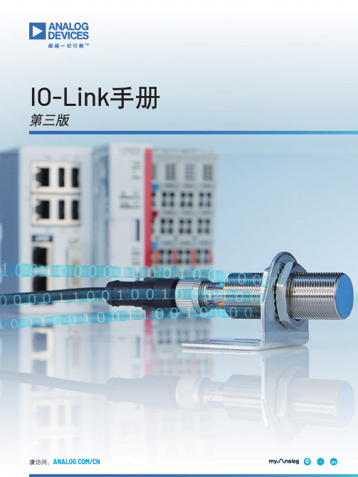
IO-Link手册第三版请访问:/CN目录引言第4页第1部分:IO-Link简介第5页◆老派传感器第5页◆微型开关量传感器驱动第5页◆I O-Link:开放式低成本传感器接口第5页◆I O-Link节点第5页◆I O-Link系统第6页◆I O-Link接口在IEC 61131-9中被标准化为SDCI第6页◆物理层IO-Link标准化接口第6页◆物理层电气规范第7页◆自动化体系中的IO-Link第7页◆I O-Link:实现智能传感器第7页◆工业传感器生态系统第8页第6部分:提高系统性能第24页◆散热第24页◆测试A第24页◆测试B第24页◆测试C第24页◆热性能第24页◆分立解决方案第25页◆集成解决方案第25页◆选择TVS二极管第25页◆I O-Link保护电路第25页◆65 V(绝对最大值)如何帮助提供保护(对比40 V)第25页◆65 V绝对最大值的保护优势第25页◆小结第26页◆I O-Link信号摆率如何影响IO-Link电缆辐射?第26页引言当今的无风扇可编程逻辑控制器(PLC)和IO-Link®网关系统须消耗大量功率,具体取决于I/O配置(IO-Link、数字输入/输出、模拟输入/输出)。
随着这些PLC演变成新的工业4.0智能工厂,我们必须深谋远虑,实现更智能、更快速、更低功耗的解决方案。
这场革命的核心是一项名为“IO-Link”的新技术,能帮助实现灵活制造,从而改善工厂吞吐量,提高运营效率。
这项激动人心的新技术正使传统传感器转变为智能传感器。
ADI公司提供一系列先进的工厂自动化解决方案,并通过我们的IO-Link技术产品系列进一步改进性能,为实现工业4.0铺路架桥。
MAX22513是该产品系列的最新成员,这是一款微型双通道IO-Link收发器,集成了浪涌保护和DC-DC转换器,可减少热耗散并提高工厂车间传感器的稳定性。
为了帮助我们的客户缩短上市时间,我们与来自IO-Link联盟的软件协议栈供应商合作开发了一系列经过全面验证和测试的参考设计,本手册对此进行了详细说明。
信息与动态

̖ڍӐૈԺय़
华为公布的《环烯烃聚合物、环烯烃聚合物单体和 光学制品的制作方法》专利技术可实现对刚性环状结构 和柔性脂肪烃基链段在聚合物中的序列分布和相对含量 的同时控制,使环烯烃聚合物兼具优异的力学性能和光 学性能。
该专利技术可以根据实际功能需要,通过在单体降 冰片烯不同位置引入烷基、芳香基、烷氧基、烃基、酯基、 氰基、氨基、硫醇基等不同的基团,获得具有不同性能 的环烯烃聚合物。长链烷基可以增加链段柔性,调节聚 合物力学性能,降低内应力;酯基、氨基等极性基团, 能增加环烯烃聚合物与其他聚合物的相容性,提高环烯 烃聚合物的可粘接性能 ; 含有环状结构和芳香基团的取 代基团,可提高材料刚性和耐热性。
发电的需求。 S&P Global Commodity Insights 的《化学经济学手
册》(CEH) 称,乐天英力士是韩国唯一的 VAM 生产商。 该公司通过在 2020 年底投产第二条生产线,将其
VAM 产能扩大了 20 万吨 / 年。 该公司于 2021 年更名为乐天英力士,当时 BP 同意
PbI2

Remnant PbI2, an unforeseen necessity in high-efficiency hybrid perovskite-based solar cells?a)Duyen H. Cao, Constantinos C. Stoumpos, Christos D. Malliakas, Michael J. Katz, Omar K. Farha, Joseph T. Hupp, and Mercouri G. KanatzidisCitation: APL Materials 2, 091101 (2014); doi: 10.1063/1.4895038View online: /10.1063/1.4895038View Table of Contents: /content/aip/journal/aplmater/2/9?ver=pdfcovPublished by the AIP PublishingArticles you may be interested inParameters influencing the deposition of methylammonium lead halide iodide in hole conductor free perovskite-based solar cellsAPL Mat. 2, 081502 (2014); 10.1063/1.4885548Air stability of TiO2/PbS colloidal nanoparticle solar cells and its impact on power efficiencyAppl. Phys. Lett. 99, 063512 (2011); 10.1063/1.3617469High efficiency mesoporous titanium oxide PbS quantum dot solar cells at low temperatureAppl. Phys. Lett. 97, 043106 (2010); 10.1063/1.3459146Near-IR activity of hybrid solar cells: Enhancement of efficiency by dissociating excitons generated in PbS nanoparticlesAppl. Phys. Lett. 96, 073505 (2010); 10.1063/1.3292183Effects of molecular interface modification in hybrid organic-inorganic photovoltaic cellsJ. Appl. Phys. 101, 114503 (2007); 10.1063/1.2737977APL MATERIALS2,091101(2014)Remnant PbI2,an unforeseen necessity in high-efficiency hybrid perovskite-based solar cells?aDuyen H.Cao,1Constantinos C.Stoumpos,1Christos D.Malliakas,1Michael J.Katz,1Omar K.Farha,1,2Joseph T.Hupp,1,band Mercouri G.Kanatzidis1,b1Department of Chemistry,and Argonne-Northwestern Solar Energy Research(ANSER)Center,Northwestern University,2145Sheridan Road,Evanston,Illinois60208,USA2Department of Chemistry,Faculty of Science,King Abdulaziz University,Jeddah,Saudi Arabia(Received2May2014;accepted26August2014;published online18September2014)Perovskite-containing solar cells were fabricated in a two-step procedure in whichPbI2is deposited via spin-coating and subsequently converted to the CH3NH3PbI3perovskite by dipping in a solution of CH3NH3I.By varying the dipping time from5s to2h,we observe that the device performance shows an unexpectedly remark-able trend.At dipping times below15min the current density and voltage of thedevice are enhanced from10.1mA/cm2and933mV(5s)to15.1mA/cm2and1036mV(15min).However,upon further conversion,the current density decreases to9.7mA/cm2and846mV after2h.Based on X-ray diffraction data,we determinedthat remnant PbI2is always present in these devices.Work function and dark currentmeasurements showed that the remnant PbI2has a beneficial effect and acts as ablocking layer between the TiO2semiconductor and the perovskite itself reducingthe probability of back electron transfer(charge recombination).Furthermore,wefind that increased dipping time leads to an increase in the size of perovskite crys-tals at the perovskite-hole-transporting material interface.Overall,approximately15min dipping time(∼2%unconverted PbI2)is necessary for achieving optimaldevice efficiency.©2014Author(s).All article content,except where otherwisenoted,is licensed under a Creative Commons Attribution3.0Unported License.[/10.1063/1.4895038]With the global growth in energy demand and with compelling climate-related environmental concerns,alternatives to the use of non-renewable and noxious fossil fuels are needed.1One such alternative energy resource,and arguably the only legitimate long-term solution,is solar energy. Photovoltaic devices which are capable of converting the photonflux to electricity are one such device.2Over the last2years,halide hybrid perovskite-based solar cells with high efficiency have engendered enormous interest in the photovoltaic community.3,4Among the perovskite choices, methylammonium lead iodide(MAPbI3)has become the archetypal light absorber.Recently,how-ever,Sn-based perovskites have been successfully implemented in functional solar cells.5,6MAPbI3 is an attractive light absorber due to its extraordinary absorption coefficient of1.5×104cm−1 at550nm;7it would take roughly1μm of material to absorb99%of theflux at550nm.Further-more,with a band gap of1.55eV(800nm),assuming an external quantum efficiency of90%,a maximum current density of ca.23mA/cm2is attainable with MAPbI3.Recent reports have commented on the variability in device performance as a function of perovskite layer fabrication.8In our laboratory,we too have observed that seemingly identicalfilmsa Invited for the Perovskite Solar Cells special topic.b Authors to whom correspondence should be addressed.Electronic addresses:j-hupp@ and m-kanatzidis@2,091101-12166-532X/2014/2(9)/091101/7©Author(s)2014FIG.1.X-ray diffraction patterns of CH3NH3PbI3films with increasing dipping time(%composition of PbI2was determined by Rietveld analysis(see Sec.S3of the supplementary material for the Rietveld analysis details).have markedly different device performance.For example,when ourfilms of PbI2are exposed to MAI for several seconds(ca.60s),then a light brown coloredfilm is obtained rather than the black color commonly observed for bulk MAPbI3(see Sec.S2of the supplementary material for the optical band gap of bulk MAPbI3).23This brown color suggests only partial conversion to MAPbI3and yields solar cells exhibiting a J sc of13.4mA/cm2and a V oc of960mV;these values are significantly below the21.3mA/cm2and1000mV obtained by others.4Under the hypothesis that fully converted films will achieve optimal light harvesting efficiency,we increased the conversion time from seconds to2h.Unexpectedly,the2-h dipping device did not show an improved photovoltaic response(J sc =9.7mA/cm2,V oc=846mV)even though conversion to MAPbI3appeared to be complete.With the only obvious difference between these two devices being the dipping time,we hypothesized that the degree of conversion of PbI2to the MAPbI3perovskite is an important parameter in obtaining optimal device performance.We thus set out to understand the correlation between the method of fabrication of the MAPbI3layer,the precise chemical compositions,and both the physical and photo-physical properties of thefilm.We report here that remnant PbI2is crucial in forming a barrier layer to electron interception/recombination leading to optimized J sc and V oc in these hybrid perovskite-based solar cells.We constructed perovskite-containing devices using a two-step deposition method according to a reported procedure with some modifications.4(see Sec.S1of the supplementary material for the experimental details).23MAPbI3-containing photo-anodes were made by varying the dipping time of the PbI2-coated photo-anode in MAI solution.In order to minimize the effects from unforeseen variables,care was taken to ensure that allfilms were prepared in an identical manner.The composi-tions offinal MAPbI3-containingfilms were monitored by X-ray diffraction(XRD).Independently of the dipping times,only theβ-phase of the MAPbI3is formed(Figure1).9However,in addition to theβ-phase,allfilms also showed the presence of unconverted PbI2(Figure1,marked with*) which can be most easily observed via the(001)and(003)reflections at2θ=12.56◦and38.54◦respectively.As the dipping time is increased,the intensities of PbI2reflections decrease with a concomitant increase in the MAPbI3intensities.In addition to the decrease in peak intensities of PbI2,the peak width increases as the dipping time increases indicating that the size of the PbI2 crystallites is decreasing,as expected,and the converse is observed for the MAPbI3reflections.This observation suggests that the conversion process begins from the surface of the PbI2crystallites and proceeds toward the center where the crystallite domain size of the MAPbI3phase increases and that of PbI2diminishes.Interestingly,the remnant PbI2phase can be seen in the data of other reports, but has not been identified as a primary source of variability in cell performance.8,10 Considering that the perovskite is the primary light absorber within the device,we wantedto further investigate how the optical absorption of thefilm changes with increasing dipping timeFIG.2.Absorption spectra of CH3NH3PbI3films as a function of unconverted PbI2phase fraction.FIG.3.(a)J-V curves and(b)EQE of CH3NH3PbI3-based devices as a function of unconverted PbI2phase fraction.(Figure2).11,12The pure PbI2film shows a band gap of2.40eV,consistent with the yellow color of PbI2.As the PbI2film is gradually converted to the perovskite,the band gap is progressively shifted toward1.60eV.The deviation of MAPbI3’s band gap(1.60eV)from that of the bulk MAPbI3 material(1.55eV)could be explained by quantum confinement effects related with the sizes of TiO2and MAPbI3crystallites and their interfacial interaction.13,14Interestingly,we also noticed the presence of a second absorption in the light absorber layer,in which the gap gradually red shifts from1.90eV to1.50eV as the PbI2concentration is decreased from9.5%to0.3%(Figure2—blue arrow).Having established the chemical compositions and optical properties of the light absorberfilms, we proceeded to examine the photo-physical responses of the corresponding functional devices in order to determine how the remnant PbI2affects device performance.The pure PbI2based device remarkably achieved a0.4%efficiency with a J sc of2.1mA/cm2and a V oc of564mV (Figure3(a)).Upon progressive conversion of the PbI2layer to MAPbI3,we observe two different regions(Figure4,Table I).In thefirst region,the expected behavior is observed;as more PbI2is converted to MAPbI3,the trend is toward higher photovoltaic efficiency,due both to J sc and V oc, until1.7%PbI2is reached.The increase in J sc is attributable,at least in part,to increasing absorption of light by the perovskite.We speculate that progressive elimination of PbI2,present as a layer between TiO2and the perovskite,also leads to higher net yields for electron injection into TiO2and therefore,higher J values.For a sufficiently thick PbI2spacer layer,electron injection would occur instepwise fashion,i.e.,perovskite→PbI2→TiO2.Finally,the photovoltage increase is attributable toFIG.4.Summary of J-V data vs.PbI2concentration of CH3NH3PbI3-based devices(Region1:0to15min dipping time, Region2:15min to2h dipping time).TABLE I.Photovoltaic performance of CH3NH3PbI3-based devices as a function of unconverted PbI2fraction.Dipping time PbI2concentration a J sc(mA/cm2)V oc(V)Fill factor(%)Efficiency(%) 0s100% 2.10.564320.45s9.5%10.10.93352 4.960s7.2%13.40.96052 6.72min 5.3%14.00.964557.45min 3.7%14.70.995578.315min 1.7%15.1 1.036629.730min0.8%13.60.968648.51h0.4%12.40.938657.62h0.3%9.70.84668 5.5a Determined from the Rietveld analysis of X-ray diffraction data.the positive shift in TiO2’s quasi-Fermi level as the population of photo-injected electrons is higher with increased concentration of MAPbI3.The second region yields a notably different trend;surprisingly,below a concentration of2% PbI2,J sc,V oc,and ultimatelyηdecrease.Considering that the light-harvesting efficiency would increase when the remaining2%PbI2is converted to MAPbI3(albeit to only a small degree),then the remnant PbI2must have some other role.We posit that remnant PbI2serves to inhibit detrimental electron-transfer processes(Figure5).Two such processes are back electron transfer from TiO2to holes in the valence band of the perovskite(charge-recombination)or to the holes in the HOMO of the HTM(charge-interception).This retardation of electron interception/recombination observation is reminiscent of the behavior of atomic layer deposited Al2O3/ZrO2layers that have been employed in dye-sensitized solar cells.15–18It is conceivable that the conversion of PbI2to MAPbI3occurs from the solution interface toward the TiO2/PbI2interface and thus would leave sandwiched between TiO2and MAPbI3a blocking layer of PbI2that inhibits charge-interception/recombination.For this hypothesis to be correct,it is crucial that the conduction-band-edge energy(E cb)of the PbI2be higher than the E cb of the TiO2.19–21 The work function of PbI2was measured by ultraviolet photoelectron spectroscopy(UPS)and was observed to be at6.35eV vs.vacuum level,which is0.9eV lower than the valence-band-edge energy(E vb)of MAPbI3(see Sec.S7of the supplementary material23for the work function of PbI2);the E cb(4.05eV)was calculated by subtracting the work function from the band gap(2.30eV).solar cell.FIG.6.Dark current of CH3NH3PbI3-based devices as a function of unconverted PbI2phase fraction.The E cb of PbI2is0.26eV higher than the E cb of TiO2and thus PbI2satisfies the conditions of a charge-recombination/interception barrier layer.In order to probe the hypothesis that PbI2acts as a charge-interception barrier,dark current measurements,in which electronsflow from TiO2to the HOMO of the HTM,were made.Consistent with our hypothesis,Figure6illustrates that the onset of the dark current occurs at lower potentials as the PbI2concentration decreases.In the absence of other effects,the increasing dark current with increasing fraction of perovskite(and decreasing fraction of PbI2)should result in progressively lower open-circuit photovoltages.Instead,the photocurrent density and the open-circuit photovoltage bothincrease,at least until to PbI2fraction reaches1.7%.As discussed above,thinning of a PbI2-basedFIG.7.Cross-sectional SEM images of CH3NH3PbI3film with different dipping time.sandwich layer should lead to higher net injection yields,but excessive thinning would diminish the effectiveness of PbI2as a barrier layer for back electron transfer reactions.Given the surprising role of remnant PbI2in these devices,we further probed the two-step conversion process by using scanning-electron microscopy(SEM)(Figure7).Two domains of lead-containing materials(PbI2and MAPbI3)are present.Thefirst domain is sited within the mesoporous TiO2network(area1)while the second grows on top of the network(area2).Area2initially contains 200nm crystals.As the dipping time is increased,the crystals show marked changes in size and morphology.The formation of bigger perovskite crystals is likely the result of the thermodynamically driven Ostwald ripening process,i.e.,smaller perovskite crystals dissolves and re-deposits onto larger perovskite crystals.22The rate of charge-interception,as measured via dark current,is proportional to the contact area between the perovskite and the HTM.Thus,the eventual formation of large, high-aspect-ratio crystals,as shown in Figure7,may well lead to increases in contact area and thereby contributes to the dark-current in Figure6.Regardless,we found that the formation of large perovskite crystals greatly decreased our success rate in constructing high-functioning,non-shorting solar cells.In summary,residual PbI2appears to play an important role in boosting overall efficiencies for CH3NH3PbI3-containing photovoltaics.PbI2’s role appears to be that of a TiO2-supported blocking layer,thereby slowing rates of electron(TiO2)/hole(perovskite)recombination,as well as decreasing rates of electron interception by the hole-transporting material.Optimal performance for energy conversion is observed when ca.98%of the initially present PbI2has been converted to the perovskite. Conversion to this extent requires about15min.Pushing beyond98%(and beyond15min of reaction time)diminishes cell performance and diminishes the success rate in constructing non-shorting cells.The latter problem is evidently a consequence of conversion of small and more-or-less uniformly packed perovskite crystallites to larger,poorly packed crystallites of varying shape and size.Finally,the essential,but previously unrecognized,role played by remnant PbI2 provides an additional explanation for why cells prepared dissolving and then depositing pre-formed CH3NH3PbI3generally under-perform those prepared via the intermediacy of PbI2.We thank Prof.Tobin Marks for use of the solar simulator and EQE measurement system. Electron microscopy was done at the Electron Probe Instrumentation Center(EPIC)at Northwestern University.Ultraviolet Photoemission Spectroscopy was done at the Keck Interdisciplinary SurfaceScience facility(Keck-II)at Northwestern University.This research was supported as part of theANSER Center,an Energy Frontier Research Center funded by the U.S Department of Energy, Office of Science,Office of Basic Energy Sciences,under Award No.DE-SC0001059.1R.Monastersky,Nature(London)497(7447),13(2013).2H.J.Snaith,J.Phys.Chem.Lett.4(21),3623(2013).3M.M.Lee,J.Teuscher,T.Miyasaka,T.N.Murakami,and H.J.Snaith,Science338(6107),643(2012).4J.Burschka,N.Pellet,S.J.Moon,R.Humphry-Baker,P.Gao,M.K.Nazeeruddin,and M.Gratzel,Nature(London) 499(7458),316(2013).5F.Hao,C.C.Stoumpos,D.H.Cao,R.P.H.Chang,and M.G.Kanatzidis,Nat.Photonics8(6),489(2014);F.Hao,C.C. Stoumpos,R.P.H.Chang,and M.G.Kanatzidis,J.Am.Chem.Soc.136,8094–8099(2014).6N.K.Noel,S.D.Stranks,A.Abate,C.Wehrenfennig,S.Guarnera,A.Haghighirad,A.Sadhanala,G.E.Eperon,M.B. Johnston,A.M.Petrozza,L.M.Herz,and H.J.Snaith,Energy Environ.Sci.7,3061(2014).7H.S.Kim,C.R.Lee,J.H.Im,K.B.Lee,T.Moehl,A.Marchioro,S.J.Moon,R.Humphry-Baker,J.H.Yum,J.E.Moser, M.Gratzel,and N.G.Park,Sci.Rep.2,591(2012).8D.Y.Liu and T.L.Kelly,Nat.Photonics8(2),133(2014).9C.C.Stoumpos,C.D.Malliakas,and M.G.Kanatzidis,Inorg.Chem.52(15),9019(2013).10J.H.Noh,S.H.Im,J.H.Heo,T.N.Mandal,and S.I.Seok,Nano Lett.13(4),1764(2013).11Diffuse reflectance measurements of MAPbI3films were converted to absorption spectra using the Kubelka-Munk equation,α/S=(1-R)2/2R,where R is the percentage of reflected light,andαand S are the absorption and scattering coefficients, respectively.The band gap values are the energy value at the intersection point of the absorption spectrum’s tangent line and the energy axis.12L.F.Gate,Appl.Opt.13(2),236(1974).13O.V oskoboynikov,C.P.Lee,and I.Tretyak,Phys.Rev.B63(16),165306(2001).14X.X.Xue,W.Ji,Z.Mao,H.J.Mao,Y.Wang,X.Wang,W.D.Ruan,B.Zhao,and J.R.Lombardi,J.Phys.Chem.C 116(15),8792(2012).15E.Palomares,J.N.Clifford,S.A.Haque,T.Lutz,and J.R.Durrant,J.Am.Chem.Soc.125(2),475(2003).16C.Prasittichai,J.R.Avila,O.K.Farha,and J.T.Hupp,J.Am.Chem.Soc.135(44),16328(2013).17A.K.Chandiran,M.K.Nazeeruddin,and M.Gratzel,Adv.Funct.Mater.24(11),1615(2014).18M.J.Katz,M.J.D.Vermeer,O.K.Farha,M.J.Pellin,and J.T.Hupp,Langmuir29(2),806(2013).19M.J.DeVries,M.J.Pellin,and J.T.Hupp,Langmuir26(11),9082(2010).20C.Prasittichai and J.T.Hupp,J.Phys.Chem.Lett.1(10),1611(2010).21F.Fabregat-Santiago,J.Garcia-Canadas,E.Palomares,J.N.Clifford,S.A.Haque,J.R.Durrant,G.Garcia-Belmonte, and J.Bisquert,J.Appl.Phys.96(11),6903(2004).22Alan D.McNaught and Andrew Wilkinson,IUPAC Compendium of Chemical Terminology(Blackwell Scientific Publica-tions,Oxford,1997).23See supplementary material at /10.1063/1.4895038for experimental details,absorption spectrum of bulk CH3NH3PbI3,fraction,size,absorption spectrum,work function of unconverted PbI2,and average photovoltaic perfor-mance.。
自考国际经济法简单题论述案例分析答案
三、简答题(本大题共3小题,每小题5分,共15分)31.简述双边投资保护协定的主要内容。
32.简述GATS法律体系的构成。
33.简述东道国对跨国银行准入的法律管制。
四、论述题(本大题共2小题,每小题15分,共30分)34.如何理解国际技术许可合同中的限制性条款?35.试述协调跨国营业所得征税权冲突的“常设机构原则”。
五、案例分析题(本大题共15分)36.2004年5月8日,一中国公司与一韩国公司签订合同订购电子部件5万套,FCA(韩国某港口)价格条件,2004年11月7日~9日交货,合同适用《联合国国际货物销售合同公约》,若发生合同争议,由中国国际经济贸易仲裁委员会仲裁解决。
后由于此类电子产品价格下跌,同年6月20日,中国公司与韩国公司将订货变更为4万套,产品价格不变。
2004年11月8日,韩国公司将货物交给中国公司指定的承运人。
11月25日,中国公司收到货物,发现韩国公司所交货物仍然是5万套。
问:(1)FCA的中文名称是什么?本案中,货物风险何时由韩国公司转移给中国公司?为什么?(2)中国公司11月25日才收到货物,能否以韩国公司未按期交货为由追究其违约责任?为什么?(3)中国公司能否按市场价收取多交的1万套电子部件?为什么?(4)若其中有万套产品不合格,中国公司想向韩国公司退换不合格产品,则在实际退回韩国公司前,中国公司应该对该部分产品采取何种措施?有关费用应由谁承担?为什么?(5)若双方纠纷经仲裁后,韩国公司拒不执行已生效的仲裁裁决,中国公司如何使裁决在韩国得到执行?法律依据是什么?一、简答题 (本大题共3小题,每小题5分,共15分)1.简述双边投资保护协定的主要内容。
答:(1)外国投资范围(或答“投资”定义也对); (2)外资准入; (3)外资待遇; (4)外资利润汇出;(5)缔约方的代位权(或答“代位”也对); (6)征收的条件及补偿标准; (7)投资争端的解决。
2.简述GATS法律体系的构成。
2012年国外有机硅进展_周勤

。
世界经济的走势也明显反映在有机硅行业。 表 1 、 表 2 分别是 2012 年几大公司有机硅业务 的销售额和利润
[2 - 9 ]
。
2012 年几大公司有机硅业务的销售额 同比增减率 / % - 4. 8 - 7. 5 3 - 4. 8 - 36. 1 15. 1 - 12. 2 26. 7 所占比例 / % 41. 5 14. 5 14. 8 9. 3 6. 5 2. 9 0. 9 1. 5 8. 1 100
表1 公司名称 道康宁
1)
界经济增长 3. 2% , 较 2011 年下降 0. 7 个百分 点。其中,美国增长 2. 3% 、欧元区降低 0. 4% 、 日本经济增长 2. 0% 、 中国增长 7. 8% , 分别较 上年 同 期 增 减 0. 5 、 - 1. 8 、 2. 6 、 - 1. 5 个 百 分点
1
市场动向
2012 年世界经济复苏道路坎坷。 欧债危机 恶化使本已脆弱的经济复苏态势再陷困境 ,发达 经济体经济增长率持续下滑,新兴市场和发展中 经济体增速放缓,财政紧缩、金融动荡、市场脆 弱令投资、就业、制造等很多经济指标无好转迹 象。根据国际货币基金组织 ( IMF) 2013 年 1 月 发布的 《世界经济展望 》 报告显示 ,2012 年世
有机硅的季度销售额和利润走势经历了年初的低 开高走到年底的以抛物线式的下滑结束的态势 ; 迈图的季度销售额和利润走势是低开高走下滑 , 到年底略有回升; 信越的季度销售额和利润走势 是高开低走。 道康宁公司 2012 年第 1 季度的销售额同比 下降 4% ,净收入同比降低 61% 。第 2 季度销售 额同比下降 6% ,净收入同比下降 36% 。第 3 季 度销售额同比下降 7% , 净收入同比下降 45% 。 第 4 季度销售额同比降低 3% ; 净收入为亏 损 1. 01 亿美元, 较上年同期 ( 2. 6 亿美元 ) 减少
美国邦纳选型指南(2012-2013)说明书

2012 - 2013 Specifier's Guide美国邦纳选型指南|PLC&HMI |光电传感器|工业安全产品|机器视觉|测量检测传感器||工业无线网络产品|工业智能指示灯|旋转编码器|激光读码器|年风雨历练 版图跨越全球美国邦纳工程国际有限公司,始建于1966年,历经近45年的风雨历练,已成为当今世界最大的工业控制器( PLC & HMI )、变频器、光电传感器、测量检测、安全产品、工业无线网络产品、机器视觉、工业智能指示灯和旋转编码器的专业制造商之一,在世界主要地区均设有世界一流的生产、销售及服务机构。
丰富的产品选择、迅速的交货期、强大的技术支持、同行业最强大的研发能力,所有这一切都确保了美国邦纳在光电领域中领先者的地位。
美国邦纳致力于为客户提供以传感为核心的综合自动化解决方案,以“创新和服务”为企业使命的美国邦纳工程公司,正凭借着世界一流的精英团队、贴心服务、优质产品、先进技术及战略性的眼光,为邦纳的新世纪版图拓展写就华彩篇章,为更多企业的发展壮大提供领先、可靠的控制和检测解决方案。
46传感器市场领导者为您的企业保驾护航过去的15年,在由第三方组织的工程师购买意向调查中,邦纳公司连续50次位于第一位。
而且“财富500强”的大多数公司的传感器也是选用的邦纳公司的产品,他们依靠着邦纳的产品顺利实现了可靠的自动化解决方案。
汽车、家电药品、食品……无论您的企业属于哪个行业,邦纳都有先进的技术、可靠的产品,帮助您实现企业生产的自动化,提高产品的生产效率和质量,为您的企业发展保驾护航。
丰富的产品线,值得您应需选择邦纳拥有超过15,000多种产品,拥有同行业内最完整的产品线,生产包括光电及超声波传感器,视觉传感器、机床安全产品、测量与检测传感器,并且可以为客户各种应用提供解决方案。
我们每天发运数千件产品,平均每3.5秒就有一个邦纳的产品被安装使用!无论您想检测或测量何种部件或材料,邦纳都可以为您提供合适的产品和解决方案。
The thermal stability of molten nitrite-nitrates salt for solar thermal energy storage_Olivares_2012

R.I. Olivares / Solar Energy 86 (2012) 2576–2583
2577
of nitrous fumes observed by Gordon and Campbell (1955), occurred at temperatures ranging from about 200–350 °C above the initial bubbling reaction. This claimed as a result of the decomposition of the nitrate and/or nitrite to oxide. The later stage of the decomposition of these nitrates was still occurring at temperatures as high as 900 °C which was the upper limit of the apparatus employed in the investigation of Gordon and Campbell (1955). Kust and Burke (1970), conducted experiments at 300 °C with a pure equimolar sodium–potassium nitrate melt in an oxygen rich atmosphere (pO2 at 0.85 atm) and measured an oxide ion ðOÀ 2 Þ concentration in the molten salt of 2 Â 10À7 molal. This was calculated by Kust to correspond to a nitrite ion ðNOÀ 2 Þ concentration of the order of 10À5 molal and demonstrated that nitrate ion ðNOÀ 3Þ could decompose to a measurable extent at temperatures as low as 295 °C. In the present work thermal decomposition was studied from at least three different points of view as follows: The temperature at which rapid weight loss is observed in a thermo-gravimetric (TG) curve. The temperature after melting at which an endothermic peak of decomposition is detected by differential scanning calorimetry in a DSC curve. The temperature at which the rapid evolution of gases, NO and/or O2, are detected by means of mass spectrometric (MS) analysis. In all these cases small to large differences are found and a judicious combination of criteria is required for practical selection of the critical salt temperature for operation in a TES field. 1.1. Theoretical considerations One of the primary concerns in the study of molten salts is the chemistry and equilibrium reactions by which the molten salt interacts with the atmosphere. 1.2. Nitrate/nitrite systems and equilibrium In nitrate based salts, the main decomposition reaction could be said to be the partial dissociation of nitrate ion À ðNOÀ 3 Þ to nitrite ion ðNO2 Þ and oxygen (O2) according to Eq. (1): Nitrate ion dissociation:
- 1、下载文档前请自行甄别文档内容的完整性,平台不提供额外的编辑、内容补充、找答案等附加服务。
- 2、"仅部分预览"的文档,不可在线预览部分如存在完整性等问题,可反馈申请退款(可完整预览的文档不适用该条件!)。
- 3、如文档侵犯您的权益,请联系客服反馈,我们会尽快为您处理(人工客服工作时间:9:00-18:30)。
SABIC向国际太阳能十项全能赛赞助LEXAN^(TM) BIPV
板
SABIC
【期刊名称】《塑料制造》
【年(卷),期】2013()11
【摘要】瑞典查尔姆斯理工大学研究生参赛队代表瑞典参加了2013中国国际太阳能十项全能竞赛,他们利用SABIC提供的轻巧而柔性的LEXAN^TM BIPV(光伏建筑一体化)板,制造了一个完全依靠太阳能运行的结构,最终在比赛中获得了奖项。
【总页数】1页(P52-52)
【关键词】BIPV;太阳能;全能;国际;光伏建筑一体化;板;研究生;瑞典
【作者】SABIC
【作者单位】
【正文语种】中文
【中图分类】TU18
【相关文献】
1.施耐德电气赞助2012年国际太阳能十项全能竞赛 [J], 无
2.ABB赞助清华大学参加“2013国际太阳能十项全能竞赛” [J],
3.打造创新型能源解决方案施耐德电气“节能梦想照进现实”——施耐德电气赞助太阳能房屋项目荣膺2012年国际太阳能十项全能竞赛欧洲赛榜首 [J], 无
4.SABIC向国际太阳能十项全能赛赞助LEXANTM BIPV板 [J], 无
5.SABIC创新LEXAN^(TM)树脂和EXATEC^(TM)涂层系统助力菲亚特全新道路版Abarth汽车点燃赛车激情 [J], Grace
因版权原因,仅展示原文概要,查看原文内容请购买。