A 1-V, 16.9 ppm C, 250 nA Switched-Capacitor CMOS Voltage Reference
LTC1606中文资料

Ext. Reference = 2.5V (Notes 12, 13) q
± 0.50
± 0.25
%
Full-Scale Error Drift
Ext. Reference = 2.5V
±2
±2
ppm/°C
Power Supply Sensitivity VANA = VDIG = VDD
VDD = 5V ±5% (Note 9)
The 90dB signal-to-noise ratio offers an improvement of 3dB over competing devices, and the RMS transition noise is reduced (0.65LSB vs 1LSB) relative to competitive parts.
CONTROL LOGIC AND
TIMING
AGND1 AGND2 DGND
2
5
14
BUSY 26 CS 25 R/C 24
BYTE 23
DIGITAL CONTROL SIGNALS
1606 TA01
Information furnished by Linear Technology Corporation is believed to be accurate and reliable. However, no responsibility is assumed for its use. Linear Technology Corporation makes no representation that the interconnection of its circuits as described herein will not infringe on existing patent rights.
电流采样运放参数

参考价/PCS 应用 1.05元/片 正泰变频器 4元/片 测试样片
8.8元/片 正泰光伏逆变器 1.5~2元/片 阿尔法英威腾、变频器 3.9元/片 LS产电
电流采样运放
品牌 型号 ST LM348 ST TL084BI 封装 S014-D S014-D TSSOP14P 输入电压 输入失调电压VIO ±15V 标准值1mV,最大5mV ±15V 标准值1mV,最大3mV ±15V ±15V ±15V ±15V 输入失调电流IiO 标准值2nA,最大25nA 标准值5pA,最大100pA
Байду номын сангаас
TI TLE2142C S014-D TI LF347N S014-D 松下 NJM3403A S014-D
标准值0.22mV,最大1.9mV 标准值8nA,最大100nA 标准值5mV,最大10mV 标准值5pA,最大100pA 标准值2mV,最大5mV 标准值5nA,最大50nA 上海洽德电子,南总监 TI代理商
电流采样运放选型参数比较品牌型号封装输入电压应用stlm348s014d15v正泰变频器sttl084bis014d15v测试样片tssop14p15vtitle2142cs014d15v正泰光伏逆变器tilf347ns014d15v阿尔法英威腾变频器松下njm3403as014d15v02166059369上海洽德电子南总监输入失调电压vio输入失调电流iio共模抑制比cmr转换速率sr增益带宽gbp参考价pcs标准值1mv最大5mv标准值2na最大25na标准值70db最大110db标准值025vus最大05vus标准值07mhz最大13mhz105元片标准值1mv最大3mv标准值5pa最大100pa最小值80db标准值86db最小值8vus标准值16vus最小值25mhz标准值4mhz标准值022mv最大19mv标准值8na最大100na最小值85db标准值118db标准值45vus标准值59mhz88元片标准值5mv最大10mv标准值5pa最大100pa最小值70db标准值100db最小值8vus标准值13vus标准值3mhz152元片标准值2mv最大5mv标准值5na最大50na最小值88db标准值100db标准值12vus标准值12mhz39元片ls产电st代理商ti代理商057188077625杭州
ADN8830中文资料
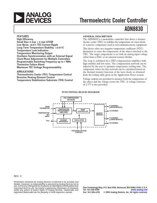
The ADN8830 is a monolithic controller that drives a thermoelectric cooler (TEC) to stabilize the temperature of a laser diode or a passive component used in telecommunications equipment. This device relies re coefficient (NTC) thermistor to sense the temperature of the object attached to the TEC. The target temperature is set with an analog input voltage either from a DAC or an external resistor divider. The loop is stabilized by a PID compensation amplifier with high stability and low noise. The compensation network can be adjusted by the user to optimize temperature settling time. The component values for this network can be calculated based on the thermal transfer function of the laser diode or obtained from the lookup table given in the Application Notes section. Voltage outputs are provided to monitor both the temperature of the object and the voltage across the TEC. A voltage reference of 2.5 V is also provided.
TDA1547中文资料
PIN 28 29 30 31 32
DESCRIPTION clock input for the left channel pin not connected; should preferably be connected to digital ground serial one-bit data input for the left channel −5 V digital supply for both channels −5 V substrate voltage
• High crosstalk immunity • Bitstream concept
– high over-sampling rate up to 192 fs – pulse-density modulation – inherently monotonic – no zero-crossing distortion
third-order noise shaper. The excellent performance of the SAA7350 and TDA1547 bitstream conversion system is obtained by separating the noise shaping circuit and the one-bit conversion circuit over two IC's, thereby reducing the crosstalk between the digital and analog parts. The TDA1547 one-bit converter is processed in BIMOS. In the digital logic and drivers bipolar transistors are used to optimize speed and to reduce digital noise generation. In the analog part the bipolar transistors are used to obtain high performance of the operational amplifiers. Special layout precautions have been taken to achieve a high crosstalk immunity. The layout of the TDA1547 has fully separated left and right channels and supply voltage lines between the digital and analog sections.
SPX3940U-3.3中文资料
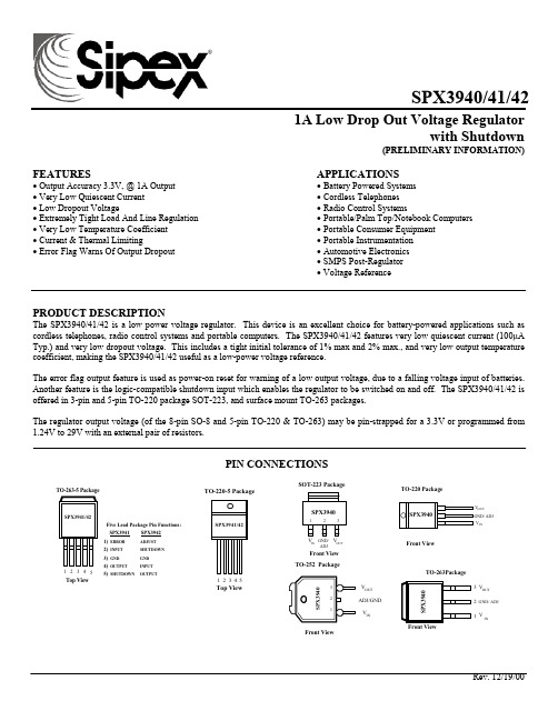
1A Low Drop Out Voltage Regulatorwith Shutdown(PRELIMINARY INFORMATION)FEATURESAPPLICATIONS• Output Accuracy 3.3V, @ 1A Output • Battery Powered Systems • Very Low Quiescent Current • Cordless Telephones • Low Dropout Voltage• Radio Control Systems• Extremely Tight Load And Line Regulation • Portable/Palm Top/Notebook Computers • Very Low Temperature Coefficient • Portable Consumer Equipment • Current & Thermal Limiting• Portable Instrumentation • Error Flag Warns Of Output Dropout • Automotive Electronics • SMPS Post-Regulator • Voltage ReferencePRODUCT DESCRIPTIONThe SPX3940/41/42 is a low power voltage regulator. This device is an excellent choice for battery-powered applications such as cordless telephones, radio control systems and portable computers. The SPX3940/41/42 features very low quiescent current (100µA Typ.) and very low dropout voltage. This includes a tight initial tolerance of 1% max and 2% max., and very low output temperature coefficient, making the SPX3940/41/42 useful as a low-power voltage reference.The error flag output feature is used as power-on reset for warning of a low output voltage, due to a falling voltage input of batteries. Another feature is the logic-compatible shutdown input which enables the regulator to be switched on and off. The SPX3940/41/42 is offered in 3-pin and 5-pin TO-220 package SOT-223, and surface mount TO-263 packages.The regulator output voltage (of the 8-pin SO-8 and 5-pin TO-220 & TO-263) may be pin-strapped for a 3.3V or programmed from 1.24V to 29V with an external pair of resistors.321V OUT GND/ ADJ V INTop View54321TO-220 PackageFront ViewV OUTINFront ViewADJ/GND V INV OUTPIN CONNECTIONSSPX3940/41/42SPX3940/41/42ABSOLUTE MAXIMUM RATINGSPower Dissipation..........................................Internally Limited Input Supply Voltage...................................................+7.5V Lead Temp. (Soldering, 5 Seconds)................................260°C Feedback Input Voltage..................................-1.5V to +30V Storage Temperature Range..............................-65° to +150°C Shutdown Input Voltage..................................-0.3V to +30V Operating Junction Temperature Range (Note 9) Error Comparator Output................................-0.3V to +30V SPX3940/41/42......................................-40C° to +125°CESD Rating ............................................................2KV MinELECTRICAL CHARACTERISTICS at V S =±15V,T A =25°C, unless otherwise specified. Boldface applies over the fulloperating temperature range.PARAMETER CONDITIONS(Note 2)Typ.SPX3940A Min Max SPX3940/41 Min Max UNITS3.3V Version Output Voltage-40°C ≤T J ≤+125°C1mA ≤I L ≤ 1A3.3 3.33.267 3.2173.333 3.3823.234 3.1853.366 3.415VAll Voltage Options Output VoltageTemperature Coefficient(Note 1)20 100 150 ppm/°CLine Regulation ( Note 3) 6V ≤ V IN ≤30V (Note 4) 20 40 60 mV Load Regulation ( Note 3 ) I L = 50mA to 1mA 35 50 80 50 80mVOutput Noise Voltage BV = 10Hz – 100kHzI L = 5mA150µV(rms)Ground Current4.5V<Vin<5.5V I L = 5mAVin=5V I L = 1A 10110 15 20200 250 15 20 200 250 mA Current LimitV OUT = 01.7 1.2 1.2 AThermal Regulation 0.05 0.2 0.2 %/wDropout Voltage (Note 5) I L = 1AI L = 100mA0.51100.8 1.0150 2000.8 1.0 150 200 V Adjustable Versions onlyTyp SPX3940/42Reference Voltage1.235 1.200 1.98 1.270 1.272VReference Voltage Over Temperature (Note 6)1.185 1.285 V Feedback Pin Bias Current20 60 80nAReference VoltageTemperature Coefficient (Note 7)50 ppm/°C Feedback Pin Bias Current Temperature Coefficient0.1nA/°CSPX3940/41/42 (Continued)PARAMETER CONDITIONS(Note 2)Typ. SPX3940/42Min MaxUNITSOutput Leakage Current V0H= 30V 0.01 1.002.00µAOutput Low Voltage V IN = 4.5VI0L = 400µA 150 250400mVUpper Threshold Voltage (Note 8) 60 4025mVLower Threshold Voltage (Note 8) 75 95140mVHysteresis (Note8) 15 mV Input logic Voltage Low (Regulator ON)High (Regulator OFF) 1.3 2.0 0.7VShut down Pin Input Current V S = 2.4VV S = 30V 30450901508001000µARegulator Output Current in Shutdown 31525µANote 1: Output or reference voltage temperature coefficients defined as the worst case voltage change divided by the total temperature range.Note 2: Unless otherwise specified all limits are guaranteed for T j = 25°C, V IN = 6V, I L = 100µA and C L = 1µF. Additional conditions for the 8-pin versions are feedback tied to 5V tap and output tied to output sense (V OUT = 5V) and V SHUTDOWN≤ 0.8V.Note 3: Regulation is measured at constant junction temperature, using pulse testing with a low duty cycle. Changes in output voltage due to heating effects are covered under the specification for thermal regulation.Note 4: Line regulation for the SPX3940/41/42 is tested at 150°C for I L = 1 mA. For I L = 100µA and T J = 125°C, line regulation is guaranteed by design to 0.2%. See typical performance characteristics for line regulation versus temperature and load current.Note 5: Dropout voltage is defined as the input to output differential at which the output voltage drops 100 mV below its nominal value measured at 1V differential at very low values of programmed output voltage, the minimum input supply voltage of 2V ( 2.3V over temperature) must be taken into account.Note 6: V REF ≤V OUT≤ (Vin - 1V), 2.3 ≤Vin≤30V, 100µA≤I L≤ 250 mA, T J ≤ T JMAX.Note 7: Comparator thresholds are expressed in terms of a voltage differential at the feedback terminal below the nominal reference voltage measured at 6V input. To express these thresholds in terms of output voltage change, multiply by the error amplifier gain = V OUT/V REF = (R1 + R2)/R2. For example, at a programmed output voltage of 5V, the Error output is guaranteed to go low when the output drops by 95 mV x 5V/1.235 = 384 mV. Thresholds remain constant as a percent of V OUT as V OUT is varied, with the dropout warning occurring at typically 5% below nominal, 7.5% guaranteed.Note 8: V SHUTDOWN≥ 2V, V IN≤ 30V, V OUT =0, Feedback pin tied to 5V Tap.Note 9: The junction -to-ambient thermal resistance of the TO-92 package is 180°C/ W with 0.4” leads and 160°C/ W with 0.25” leads to a PC board.The thermal resistance of the 8-Pin DIP package is 105°C/W junction-to-ambient when soldered directly to a PC board. Junction-to-ambient thermal resistance for the SOIC (S) package is 160°C/W.APPLICATION HINTSEXTERNAL CAPACITORSThe stability of the SPX3940/41/42 requires a 2.2µF or greater capacitor between output and ground. Oscillation could occur without this capacitor. Most types of tantalum or aluminum electrolytic works fine here. For operations of below -25°C solid tantalum is recommended since the many aluminum types have electrolytes the freeze at about -30°C. The ESR of about 5Ω or less and resonant frequency above 500kHz are the most important parameters in the value of the capacitor. The capacitor value can be increased without limit.At lower values of output current, less output capacitance is required for stability. For the currents below 10mA the value of the capacitor can be reduced to 0.5µF and 0.15µF for 1A. More output capacitance needed for the 8-pin version at voltages below 5V since it runs the error amplifier at lower gain. At worst case 5µF or greater must be used for the condition of 250mA load at 1.23V output.The SPX3940/41/42, unlike other low dropout regulators will remain stable and in regulation with no load in addition to the internal voltage divider. This feature is especially important in application like CMOS RAM keep-alive. When setting the output voltage of the SPX3940/41/42, a minimum load of 10mA is recommended.If there is more than 10 inches of wire between the input and the AC filter capacitor or if a battery is used as the input then a 0.1µF tantalum or aluminum electrolytic capacitor should be placed from the input to the ground.Instability can occur if there is stray capacitance to the SPX3940/41/42 feedback terminal (pin 7). This could cause more problems when using a higher value of external resistors to set the output voltage.This problem can be fixed by adding a 100pF capacitor between output and feedback and increasing the output capacitor to at least 3.3µF.ERROR DETECTION COMPARATOR OUTPUTThe Comparator produces a logic low output whenever the SPX3940/41/42 output falls out of regulation by more than around 5%. This is around 60mV offset divided by the 1.235 reference voltage. This trip level remains 5% below normal regardless of the programmed output voltage of the regulator. Figure 1 shows the timing diagram depicting the ERROR signal and the regulator output voltage as the SPX3940/41/42 input is ramped up and down. The ERROR signal becomes low at around 1.3V input, and goes high around 5V input (input voltage at which Vout = 4.75). Since the SPX3940/41/42’s dropout voltage is load dependent, the input voltage trip point (around 5V) will vary with the load current. The output voltage trip point (approx. 4.75V) does not vary with load.The error comparator has an open-collector output, which requires an external pull-up resistor. Depending on the system requirements the resistor may be returned to 5V output or other supply voltage. In determining the value of this resistor, note that the output is rated to sink 400µA, this value adds to battery drain in a low battery condition. Suggested values range from 100K to 1M Ω. If the output is unused this resistor is not required.PROGRAMMING THE OUTPUT VOLTAGE OF SPX3940/41/42The SPX3940/41/42 may be pin-strapped for 5V using its internal voltage divider by tying Pin 1 (output) to Pin 2 (sense) and Pin 7 (feedback) to Pin 6 (5V Tap).++++4.75VO U T PU T V O L T A G E E R R O R *_______IN P U T V O L T A G E1.3V5.0VF ig u r e 1. E R R O R O u tp u t T im in g_______* S ee A p p licatio n In fo.Also, it may be programmed for any output voltage between its 1.235V reference and its 30V maximum rating. As seen in Figure 2, an external pair of resistors is required.Refer to the below equation for the programming of the output voltage::V OUT = V REF× ( 1 + R1\ R2 )+ I FB R1The V REF is 1.235 and I FB is the feedback bias current, nominally -20nA. The minimum recommended load current of 1 µA forces an upper limit of 1.2 MΩ on value of R2.If no load is presented the I FB produces an error of typically 2% in V OUT, which may be eliminated at room temperature by trimming R1. To improve the accuracy choose the value of R2 = 100k this reduces the error by 0.17% and increases the resistor program current by 12µA. Since the LP2951 typically draws 60 µA at no load with Pin 2 open-circuited this is a small price to pay REDUCING OUTPUT NOISEIt may be an advantage to reduce the AC noise present at the output. One way is to reduce the regulator bandwidth by increasing the size of the output capacitor. This is the only way that noise can be reduced on the 3 lead SPX3940/41/42 but is relatively inefficient, as increasing the capacitor from 1µF to 220µF only decreases the noise from 430µV to 160µV Vrms for a 100kHz bandwidth at 5V output. Noise could also be reduced fourfold by a bypass capacitor across R1, since it reduces the high frequency gain from 4 to unity. PickC BYPASS ≅ 1 / 2πR1× 200 Hzor choose 0.01µF. When doing this, the output capacitor must be increased to 3.3µF to maintain stability. These changes reduce the output noise from 430µV to 100µV Vrms for a 100kHz bandwidth at 5V output. With the bypass capacitor added, noise no longer scales with output voltage so that improvements are more dramatic at higher output voltages.HEAT SINK REQUIREMENTSDepending on the maximum ambient temperature and maximum power dissipation a heat sink may be required with the SPX3940/41/42. The junction temperature range has to be within the range specified under Absolute Maximum Ratings under all possible operating conditions. To find out if a heat sink is required, the maximum power dissipation of the device needs to be calculated. This is the maximum specific AC voltage that must be taken into consideration at input. Figure 3 shows thecondition and power dissipation which should be calculated with the following formula:P TOTAL = (V IN - 5) I L + (V IN)I GNext step is to calculate the temperature rise T R (max). T J (max) maximum allowable junction temperature, T A (max) maximum ambient temperature :T R (max) = T J (max) - T A (max)Junction to ambient thermal resistance θ(j-A) can be calculated after determining of P TOTAL & T R (max):θ(J-A) = T R (max)/P(max)If the θ(J-A) is 60°C/W or higher, the device could be operated without a heat sink. If the value is below 60°C/W then the heat sink is required and the thermal resistance of the heat sink can be calculated by the following formula, θ(J-C) junction to case, θ(C-H) case to heat sink, θ(H-A) heat sink to ambient:θ(J-A) = θ(J-C) + θ(C-H) + θ(H-A)Figure 3. 3.3V Regulator CircuitTYPICAL APPLICATIONSORDERING INFORMATIONOrdering No. Precision Output Voltage PackagesSPX3940AM3 1% Adj 3 Lead SOT-223SPX3940AM3-3.3 1% 3.3V 3 Lead SOT-223SPX3940AM3-5.0 1% 5.0V 3 Lead SOT-223SPX3940M3 2% Adj 3 Lead SOT-223SPX3940M3-3.3 2% 3.3V 3 Lead SOT-223SPX3940M3-5.0 2% 5.0V 3 Lead SOT-223SPX3940AR 1% Adj 5 Lead TO-252SPX3940AR-3.3 1% 3.3V 3 Lead TO-252SPX3940AR-5.0 1% 5.0V 3 Lead TO-252SPX3940R 2% Adj 5 Lead TO-252SPX3940R-3.3 2% 3.3V 3 Lead TO-252SPX3940R-5.0 2% 5.0V 3 Lead TO-252SPX3940AU 1% Adj 5 Lead TO-220SPX3940AU-3.3 1% 3.3V 3 Lead TO-220SPX3940AU-5.0 1% 5.0V 3 Lead TO-220SPX3940U 2% Adj 5 Lead TO-220SPX3940U-3.3 2% 3.3V 3 Lead TO-220SPX3940U-5.0 2% 5.0V 3 Lead TO-220SPX3940AT 1% Adj 5 Lead TO-263SPX5940AT-3.3 1% 3.3V 3 Lead TO-263SPX3940AT-5.0 1% 5.0V 3 Lead TO-263SPX3940T 2% Adj 5 Lead TO-263SPX3940T-3.3 2% 3.3V 3 Lead TO-263SPX3940T-5.0 2% 5.0V 3 Lead TO-263SPX3941R-3.3 2% 3.3V 3 Lead TO-252SPX3941R-5.0 2% 5.0V 3 Lead TO-252SPX3941U-3.3 2% 3.3V 3 Lead TO-220SPX3941U-5.0 2% 5.0V 3 Lead TO-220SPX3941T-3.3 2% 3.3V 3 Lead TO-263SPX3941T-5.0 2% 5.0V 3 Lead TO-263SPX3942R 2% Adj 5 Lead TO-252SPX3942U 2% Adj 3 Lead TO-220SPX3942T 2% Adj 3 Lead TO-263CorporationSIGNAL PROCESSING EXCELLENCESipex CorporationHeadquarters and Main Offices:22 Linnell CircleBillerica, MA 01821TEL: (978) 667-8700FAX: (978) 670-9001e-mail: sales@233 South Hillview DriveMilpitas, CA 95035TEL: (408) 935-7600FAX: (408) 934-7500Sipex Corporation reserves the right to make changes to any products described herein. Sipex does not assume any liability arising out of the application or use of any product or circuit described hereing; neither does it convey any license under its patent rights nor the rights of others.。
6N135中文资料
Single Channel, High Speed Optocouplers Technical DataFeatures• 15 kV/µs Minimum Common Mode Transient Immunity at V CM = 1500 V (4503/0453)• High Speed: 1 Mb/s • TTL Compatible• Available in 8-Pin DIP, SO-8,Widebody Packages • Open Collector Output • Guaranteed Performance from Temperature: 0°C to 70°C• Safety ApprovalUL Recognized – 3750 V rms for 1 minute (5000 V rms for 1 minute for HCNW and Option 020 devices) per UL1577CSA ApprovedIEC/EN/DIN EN 60747-5-2Approved–V IORM = 630 V peak for HCPL-4503#060–V IORM = 1414 V peak for HCNW devices• Dual Channel VersionAvailable (253X/4534/053X/0534)• MIL-PRF-38534 Hermetic Version Available (55XX/65XX/4N55)Applications• High Voltage Insulation • Video Signal Isolation• Power Transistor Isolation in Motor Drives • Line Receivers• Feedback Element in Switched Mode Power Supplies• High Speed Logic Ground Isolation – TTL/TTL, TTL/CMOS, TTL/LSTTL• Replaces Pulse Transformers • Replaces SlowPhototransistor Isolators • Analog Signal Ground IsolationDescriptionThese diode-transistor optocoup-lers use an insulating layerbetween a LED and an integrated photodetector to provide elec-trical insulation between input and output. Separate connections for the photodiode bias and output-transistor collector increase the speed up to ahundred times that of a conven-tional phototransistor coupler by reducing the base-collector capacitance.Functional Diagram6N135/6HCNW135/6HCNW4502/3HCPL-2502HCPL-0452/3HCPL-0500/1HCPL-4502/3CAUTION: It is advised that normal static precautions be taken in handling and assembly of this component to prevent damage and/or degradation which may be induced by ESD.A 0.1 µF bypass capacitor must be connected between pins 5 and 8.V CC V B V O GND** NOTE: FOR 4502/3, 0452/3,PIN 7 IS NOT CONNECTED.TRUTH TABLE (POSITIVE LOGIC)LEDONOFFV O LOW HIGHGNDV CCOANODECATHODEB* NOTE: FOR HCPL-4502/-3, HCPL-0452/3, HCNW4502/3, PIN 7 IS NOT CONNECTED.Ordering InformationSpecify Part Number followed by Option Number (if desired).Example:HCPL-4503#XXXX020 =UL 5000 V rms/1 Minute Option*060 =IEC/EN/DIN EN 60747-5-2 V IORM = 630 V peak Option**300 =Gull Wing Surface Mount Option†500 =Tape and Reel Packaging Option XXXE = Lead Free OptionOption data sheets available. Contact your Agilent sales representative or authorized distributor for information.*For 6N135/6 and HCPL-4502/3 only.**For HCPL-4503 only. Combination of Option 020 and Option 060 is not available.†Gull wing surface mount option applies to through hole parts only.*Technical data for these products are on separate Agilent publications.†Pin 7, transistor base, is not connected.output current for 1 TTL load and a 5.6 k Ω pull-up resistor. CTR for these devices is 19% minimum at I F =16mA.The HCPL-4502, HCPL-0452,and HCNW4502 provide the electrical and switching performance of the 6N136,HCPL-0501, and HCNW136 with increased ESD protection.The HCPL-4503, HCPL-0453,and HCNW4503 are similar to the HCPL-4502, HCPL-0452, and HCNW4502 optocouplers but have increased common mode transient immunity of 15 kV/µs minimum at V CM =1500V guaranteed.These single channel optocoup-lers are available in 8-Pin DIP,SO-8 and Widebody package configurations.The 6N135, HCPL-0500, and HCNW135 are for use in TTL/CMOS, TTL/LSTTL or wide bandwidth analog applications.Current transfer ratio (CTR) for these devices is 7% minimum at I F =16mA.The 6N136, HCPL-2502,HCPL-0501, and HCNW136 are designed for high speed TTL/TTL applications. A standard 16 mA TTL sink current through the input LED will provide enoughRemarks: The notation “#” is used for existing products, while (new) products launched since 15th July 2001 and lead free option will use “-”Package Outline Drawings8-Pin DIP Package (6N135/6, HCPL-4502/3, HCPL-2502)8-Pin DIP Package with Gull Wing Surface Mount Option 300 (6N135/6, HCPL-4502/3)0.254+ 0.076- 0.051(0.010+ 0.003)- 0.002)DIMENSIONS IN MILLIMETERS AND (INCHES).*MARKING CODE LETTER FOR OPTION NUMBERS "L" = OPTION 020"V" = OPTION 060OPTION NUMBERS 300 AND 500 NOT MARKED.NOTE: FLOATING LEAD PROTRUSION IS 0.25 mm (10 mils) MAX.(0.025 ± 0.005)(0.100)BSCDIMENSIONS IN MILLIMETERS (INCHES).LEAD COPLANARITY = 0.10 mm (0.004 INCHES).NOTE: FLOATING LEAD PROTRUSION IS 0.25 mm (10 mils) MAX.+ 0.076- 0.051+ 0.003)- 0.002)Small Outline SO-8 Package (HCPL-0500/1, HCPL-0452/3)8-Pin Widebody DIP Package (HCNW135/6, HCNW4502/3)(0.012)MIN.5.207 ± 0.254 (0.205 ± 0.010)DIMENSIONS IN MILLIMETERS (INCHES).LEAD COPLANARITY = 0.10 mm (0.004 INCHES) MAX.*1.78 ± 0.15NOTE: FLOATING LEAD PROTRUSION IS 0.25 mm (10 mils) MAX.0.254+ 0.076- 0.0051+ 0.003)- 0.002)8-Pin Widebody DIP Package with Gull Wing Surface Mount Option 300 (HCNW135/6,HCNW4502/3)Solder Reflow Temperature ProfileTIME (SECONDS)T E M P E R A T U R E (°C )ROOM1.78 ± 0.15MAX.BSCDIMENSIONS IN MILLIMETERS (INCHES).LEAD COPLANARITY = 0.10 mm (0.004 INCHES).NOTE: FLOATING LEAD PROTRUSION IS 0.25 mm (10 mils) MAX.Regulatory InformationThe devices contained in this data sheet have been approved by the following organizations:ULRecognized under UL 1577,Component Recognition Program, File E55361.CSAApproved under CSA Component Acceptance Notice #5, File CA 88324.Insulation and Safety Related Specifications8-Pin DIP Widebody (300 Mil)SO-8(400 Mil)Parameter Symbol Value Value Value Units ConditionsMinimum External L(101)7.14.99.6mmMeasured from input terminals Air Gap (External to output terminals, shortest Clearance)distance through air.Minimum External L(102)7.4 4.810.0mmMeasured from input terminals Tracking (External to output terminals, shortest Creepage)distance path along body.Minimum Internal 0.080.08 1.0mmThrough insulation distance,Plastic Gapconductor to conductor, usually (Internal Clearance)the direct distance between the photoemitter and photodetector inside the optocoupler cavity.Minimum Internal NA NA 4.0mmMeasured from input terminals Tracking (Internal to output terminals, along Creepage)internal cavity.Tracking Resistance CTI 200200200VoltsDIN IEC 112/VDE 0303 Part 1(Comparative Tracking Index)Isolation GroupIIIa IIIa IIIaMaterial Group(DIN VDE 0110, 1/89, Table 1)Option 300 - surface mount classification is Class A in accordance with CECC 00802.IEC/EN/DIN EN 60747-5-2Approved underIEC 60747-5-2:1997 + A1:2002EN 60747-5-2:2001 + A1:2002DIN EN 60747-5-2 (VDE 0884 Teil 2):2003-01(HCNW and Option 060 only)Recommended Pb-Free IR Profile°C of ACTUAL NOTES:THE TIME FROM 25 °C to PEAK TEMPERATURE = 8 MINUTES MAX.T smax = 200 °C, T smin = 150 °CIEC/EN/DIN EN 60747-5-2 Insulation Related Characteristics(HCPL-4503 OPTION 060 ONLY)IEC/EN/DIN EN 60747-5-2 Insulation Related Characteristics (HCNW135/6, HCNW4502/3 ONLY)*Refer to the front of the optocoupler section of the current catalog, under Product Safety Regulations section IEC/EN/DIN EN60747-5-2, for a detailed description.Note: Isolation characteristics are guaranteed only within the safety maximum ratings which must be ensured by protective circuits in application.*Data has been registered with JEDEC for the 6N135/6N136.Electrical Specifications (DC)Over recommended temperature (T A = 0°C to 70°C) unless otherwise specified. See note 13.Parameter Symbol Device Min.Typ.**Max.Units Test Conditions Fig.Note Current CTR*6N13571850%T A = 25°C V O = 0.4 V I F = 16 mA,1, 2,5, 11 Transfer Ratio HCPL-0500V CC = 4.5 V4HCNW135519V O = 0.5 VHCPL-25021522T A = 25°C V O = 0.4 V1525V O = 0.5 V6N136192450T A = 25°C V O = 0.4 VHCPL-4502/3HCPL-05011525V O = 0.5 VHCPL-0452/3HCNW136HCNW4502/3Logic Low V OL6N1350.10.4V T A = 25°C I O = 1.1 mA I F = 16 mA,Output Voltage HCPL-0500V CC = 4.5 VHCNW1350.10.5I O = 0.8 mA6N1360.10.4T A = 25°C I O = 3.0 mAHCPL-2502HCPL-4502/30.10.5I O = 2.4 mAHCPL-0501HCPL-0452/3HCNW136HCNW4502/3Logic High I OH*0.0030.5µA T A = 25°C V O = V CC = 5.5 V I F = 0 mA7Output Current0.011T A = 25°C V O = V CC = 15 V50V O = V CC = 15 VLogic Low I CCL50200µA I F = 16 mA, V O = Open, V CC = 15 V13 Supply CurrentLogic High I CCH*0.021µA T A = 25°C I F = 16 mA, V O = Open,13 Supply Current2V CC = 15 VInput Forward V F*8-Pin DIP 1.5 1.7V T A = 25°C I F = 16 mA3Voltage SO-8 1.8Widebody 1.45 1.68 1.85T A = 25°C I F = 16 mA1.35 1.95Input Reverse BV R*8-Pin DIP5V I R = 10 µABreakdown SO-8Voltage Widebody3I R = 100 µATemperature∆V F/8-Pin DIP-1.6mV/°C I F = 16 mACoefficient of∆T A SO-8Forward Voltage Widebody-1.9Input C IN8-Pin DIP60pF f = 1 MHz, V F = 0 VCapacitance SO-8Widebody90Transistor DC h FE8-Pin DIP150V O = 5 V, I O = 3 mACurrent Gain SO-8130V O = 0.4 V, I B = 20 µAWidebody180V O = 5 V, I O = 3 mA160V O = 0.4 V, I B = 20 µA*For JEDEC registered parts.**All typicals at T A = 25°C.Parameter Sym.Device Min.Typ.**Max.Units Test ConditionsFig.Note Propagation t PHL *6N1350.2 1.5µs T A = 25°C R L = 4.1 k Ω5, 6,8, 9HCPL-0500 2.011HCNW1356N1360.20.8T A = 25°C R L = 1.9 k ΩHCPL-2502HCPL-4502/3HCPL-0501HCPL-0452/3 1.0HCNW136HCNW4502/3Propagation t PLH *6N135 1.3 1.5µsT A = 25°C R L = 4.1 k Ω5, 6,8, 9HCPL-0500 2.011HCNW1356N1360.60.8T A = 25°C R L = 1.9 k ΩHCPL-2502HCPL-4502/3HCPL-0501HCPL-0452/3 1.0HCNW136HCNW4502/3Common Mode |CM H |6N1351kV/µs R L = 4.1 k ΩI F = 0 mA, T A = 25°C,127, 8,HCPL-0500V CM = 10 V p-p 9HCNW135C L = 15 pF6N1361R L = 1.9 k ΩHCPL-2502HCPL-4502HCPL-0501HCPL-0452HCNW4502HCPL-45031530R L = 1.9 k ΩI F = 0 mA, T A = 25°C,HCPL-0453V CM = 1500 V p-p ,HCNW4503C L = 15 pFCommon Mode |CM L |6N1351kV/µs R L = 4.1 k ΩI F = 16 mA, T A = 25°C,127, 8,HCPL-0500V CM = 10 V p-p 9HCNW135C L = 15 pF6N1361R L = 1.9 k ΩHCPL-2502HCPL-4502HCPL-0501HCPL-0452HCNW4502HCPL-45031530R L = 1.9 k ΩI F = 16 mA, T A = 25°C,HCPL-0453V CM = 1500 V p-p ,HCNW4503C L = 15 pFBandwidth BW 6N135/69MHzSee Test Circuit8, 1010HCPL-2502HCPL-0500/1HCNW135/611*For JEDEC registered parts.**All typicals at T A = 25°C.Switching Specifications (AC)Over recommended temperature (T A = 0°C to 70°C), V CC = 5 V, I F = 16 mA unless otherwise specified.Delay Time to Logic Low at OutputDelay Time to Logic High at OutputTransient Immunity at Logic High Level OutputTransient Immunity at Logic Low Level OutputPackage CharacteristicsOver recommended temperature (T A = 0°C to 70°C) unless otherwise specified.*All typicals at T A = 25°C.**The Input-Output Momentary Withstand Voltage is a dielectric voltage rating that should not be interpreted as an input-output continuous voltage rating. For the continuous voltage rating refer to the IEC/EN/DIN EN 60747-5-2 Insulation Related Characteristics Table (if applicable), your equipment level safety specification or Agilent Application Note 1074 entitled “Optocoupler Input-Output Endurance Voltage,” publication number 5963-2203E.Notes:1.Derate linearly above 70°C free-air temperature at a rate of 0.8 mA/°C (8-Pin DIP).Derate linearly above 85°C free-air temperature at a rate of 0.5 mA/°C (SO-8).2.Derate linearly above 70°C free-air temperature at a rate of 1.6 mA/°C (8-Pin DIP).Derate linearly above 85°C free-air temperature at a rate of 1.0 mA/°C (SO-8).3.Derate linearly above 70°C free-air temperature at a rate of 0.9 mW/°C (8-Pin DIP).Derate linearly above 85°C free-air temperature at a rate of 1.1 mW/°C (SO-8).4.Derate linearly above 70°C free-air temperature at a rate of 2.0 mW/°C (8-Pin DIP).Derate linearly above 85°C free-air temperature at a rate of 2.3 mW/°C (SO-8).5.CURRENT TRANSFER RATIO in percent is defined as the ratio of output collector current, I O, to the forward LED input current, I F,times 100.6.Device considered a two-terminal device: Pins 1, 2, 3, and 4 shorted together and Pins 5, 6, 7, and 8 shorted together.mon mode transient immunity in a Logic High level is the maximum tolerable (positive) dV CM/dt on the leading edge of thecommon mode pulse signal, V CM, to assure that the output will remain in a Logic High state (i.e., V O > 2.0 V). Common mode transient immunity in a Logic Low level is the maximum tolerable (negative) dV CM/dt on the trailing edge of the common mode pulse signal, V CM, to assure that the output will remain in a Logic Low state (i.e., V O < 0.8 V).8.The 1.9 kΩ load represents 1 TTL unit load of 1.6 mA and the 5.6 kΩ pull-up resistor.9.The 4.1 kΩ load represents 1 LSTTL unit load of 0.36 mA and 6.1 kΩ pull-up resistor.10.The frequency at which the ac output voltage is 3 dB below its mid-frequency value.11.The JEDEC registration for the 6N136 specifies a minimum CTR of 15%. Agilent guarantees a minimum CTR of 19%.12.See Option 020 data sheet for more information.e of a 0.1 µf bypass capacitor connected between pins 5 and 8 is recommended.14.In accordance with UL 1577, each optocoupler is proof tested by applying an insulation test voltage ≥ 4500 V rms for 1 second(leakage detection current limit, I I-O≤ 5 µA). This test is performed before the 100% Production test shown in the IEC/EN/DIN EN 60747-5-2 Insulation Related Characteristics Table if applicable.15.In accordance with UL 1577, each optocoupler is proof tested by applying an insulation test voltage ≥ 6000 V rms for 1 second(leakage detection current limit, I I-O≤ 5 µA). This test is performed before the 100% Production test shown in the IEC/EN/DIN EN 60747-5-2 Insulation Related Characteristics Table if applicable.16.This rating is equally validated by an equivalent ac proof test.Figure 2. Current Transfer Ratio vs. Input Current.Figure 3. Input Current vs. Forward Voltage.Figure 1. DC and Pulsed Transfer Characteristics.105V O – OUTPUT VOLTAGE – VI O – O U T P U T C U R R E N T – m A8 PIN DIP, SO-8128V O – OUTPUT VOLTAGE – VI O – O U T P U T C U R R E N T – m A416WIDEBODY1.51.00.5N O R M A L I Z E D C U R R E N T T R A N S F E R R A T I OI F – INPUT CURRENT – mA8 PIN DIP, SO-80N O R M A L I Z E D C U R R E N T T R A N S F E R R A T I OI F – INPUT CURRENT – mA1.50.51.0WIDEBODYV F – FORWARD VOLTAGE –VOLTS I F – F O R W A R D C U R R E N T – m A8 PIN DIP, SO-8V F –FORWARD VOLTAGE – VOLTS1000100101.00.10.001I F – F O R W A R D C U R R E N T – m AWIDEBODYFigure 6. Propagation Delay Time vs. Load Resistance.Figure 5. Propagation Delay vs. Temperature.Figure 4. Current Transfer Ratio vs. Temperature.1.00.90.80.70.6N O R M A L I Z E D C U R R E N T T R A N S F E R R A T I OT A – TEMPERATURE – °C 8 PIN DIP, SO-81.11.00.90.80.70.660N O R M A L I Z E D C U R R E N T T R A N S F E R R A T I OT A – TEMPERATURE – °C0.50.4WIDEBODY1.0R L – LOAD RESISTANCE – (k Ω)t P – P R O P A G A T I O N D E L A Y – µs8 PIN DIP, SO-8R L – LOAD RESISTANCE – (k Ω)t P – P R O P A G A T I O N D E L A Y – µs6.04.01.00.60.40.2WIDEBODY150010005000t p – P R O P A G A T I O N D E L A Y – n sT A – TEMPERATURE – °C 8 PIN DIP, SO-81000800600400200T A – TEMPERATURE – °CWIDEBODYt p – P R O P A G A T I O N D E L A Y – n sFigure 9. Thermal Derating Curve, Dependence of Safety Limiting Value with Case Temperature per IEC/EN/DIN EN 60747-5-2.Figure 8. Small-Signal Current Transfer Ratio vs. Quiescent Input Current.Figure 7. Logic High Output Current vs. Temperature.T A – TEMPERATURE – °C10+410101001010+210+3I O H – L O G I C H I G H O U T P U T C U R R E N T – n A8 PIN DIP, SO-8I O H– L O G I C H I G H O U T P U T C U R R E N T – n AT A – TEMPERATURE – °C10101010WIDEBODY∆ I F∆I O – S M A L L S I G N A L C U R R E N T T R A N S F E R R A T I O I F – QUIESCENT INPUT CURRENT – mA 8 PIN DIP, SO-80.30∆ I F ∆ I O– S M A L L S I G N A L C U R R E N T T R A N S F E R R A T I OI F – QUIESCENT INPUT CURRENT – mAWIDEBODYO U T P U TP O W E R – P S , I N P U T C U R R E N T – I ST S – CASE TEMPERATURE – °C O U T P U T P OW E R – P S , I N P U T C U R R E N T – I S0T S – CASE TEMPERATURE – °C1000400600800200100300500700900Figure 10. Frequency Response.HCNW135/6HCNW135/60.11.010100-20-15-10-5+5T A = 25 °Cf - FREQUENCY - MHzN O R M A L I Z E D R E S P O N S E - d B6N135/6, HCPL-0500/1, HCPL-2502V TYPICAL I = 9 mA FO6N135/6, HCPL-0500/1, HCPL-2502Figure 12. Test Circuit for Transient Immunity and Typical Waveforms.Figure 11. Switching Test Circuit.OF= 1.5 µFt V I F OVOV O/semiconductorsFor product information and a complete list ofdistributors, please go to our web site.For technical assistance call:Americas/Canada: +1 (800) 235-0312 or (916) 788-6763Europe: +49 (0) 6441 92460China: 10800 650 0017Hong Kong: (+65) 6756 2394India, Australia, New Zealand: (+65) 6755 1939Japan: (+81 3) 3335-8152 (Domestic/Interna-tional), or 0120-61-1280 (Domestic Only)Korea: (+65) 6755 1989Singapore, Malaysia, Vietnam, Thailand,Philippines, Indonesia: (+65) 6755 2044Taiwan: (+65) 6755 1843Data subject to change.Copyright © 2004 Agilent Technologies, Inc.Obsoletes 5989-0305EN December 20, 20045989-2112EN。
TPS61170资料
FEATURESDESCRIPTIONAPPLICATIONSL1L1:TOKO#A915_Y-100MC1: Murata GRM188R61A475K C2: Murata GRM21BR61E475K D1:ONsemi MBR0540T1*R3, C3: Compensation RC networkTPS61170SLVS789–NOVEMBER 20071.2A High Voltage Boost Converter in 2x2mm 2QFN Package•3-V to 18-V Input Voltage Range •High Output Voltage:Up to 38V The TPS61170is a monolithic high voltage switching regulator with integrated 1.2-A,40-V power MOSFET.• 1.2-A integrated SwitchIt can be configured in several standard • 1.2-MHz Fixed Switching Frequencyswitching-regulator topologies,including boost and •12V at 300mA and 24V at 150mA from 5-V SEPIC.The device has a wide input-voltage range to Input (Typical)support applications with input voltage from multi-cell batteries or regulated 5-V,12-V power rails.•Up to 93%EfficiencyThe TPS61170uses a 1.2-MHz switching frequency,•On-The-Fly Output Voltage Reprogramming allowing the use low-profile inductors and low-value •Skip-Switching Cycle for Output Regulation at ceramic input and output capacitors.The external Light Loadloop compensation gives the user flexibility to •Built-in Soft Startoptimize loop compensation and transient response.The device has built-in protection features,such as •6-Pin,2mm ×2mm QFN Packagepulse-by-pulse overcurrent limit,soft start and thermal shutdown.•5-V to 12-V and 24-V,12-V to 24-V Boost The feedback reference voltage of the FB pin is Converter1.229V.It can be lowered using a 1-wire digital interface (Easyscale™protocol)through the CTRL •Buck Boost Regulation Using SEPIC Topology pin.Alternatively,a pulsewidth-modulation (PWM)•ADSL Modemssignal can be applied to the CTRL pin.The duty cycle of the signal reduces the feedback reference voltage proportionally.The TPS61170is available in a 6-pin 2mm ×2mm QFN package,allowing a compact power-supply solution.Figure 1.Typical ApplicationPlease be aware that an important notice concerning availability,standard warranty,and use in critical applications of Texas Instruments semiconductor products and disclaimers thereto appears at the end of this data sheet.PRODUCTION DATA information is current as of publication date.Copyright ©2007,Texas Instruments IncorporatedProducts conform to specifications per the terms of the Texas Instruments standard warranty.Production processing does not necessarily include testing of all parameters.ABSOLUTE MAXIMUM RATINGSDISSIPATION RATINGSRECOMMENDED OPERATING CONDITIONSTPS61170SLVS789–NOVEMBER 2007These devices have limited built-in ESD protection.The leads should be shorted together or the device placed in conductive foam during storage or handling to prevent electrostatic damage to the MOS gates.ORDERING INFORMATION (1)T APACKAGE (2)PACKAGE MARKING–40°C to 85°CTPS61170DRVBZS(1)For the most current package and ordering information,see the TI Web site at .(2)The DRV package is available in tape and reel.Add R suffix (TPS61170DRVR)to order quantities of 3000parts per reel or add T suffix (TPS61170DRVT)to order 250parts per reel.over operating free-air temperature range (unless otherwise noted)(1)VALUE UNIT Supply Voltages on VIN(2)–0.3to 20V Voltages on CTRL (2)–0.3to 20V V IVoltage on FB and COMP(2)–0.3to 3V Voltage on SW (2)–0.3to 40V P D Continuous Power DissipationSee Dissipation Rating TableT J Operating Junction Temperature Range –40to 150°C T STG Storage Temperature Range–65to 150°C(1)Stresses beyond those listed under absolute maximum ratings may cause permanent damage to the device.These are stress ratings only,and functional operation of the device at these or any other conditions beyond those indicated under recommended operating conditions is not implied.Exposure to absolute-maximum-rated conditions for extended periods may affect device reliability.(2)All voltage values are with respect to network ground terminal.DERATING FACTOR BOARD PACKAGER θJC R θJA T A <25°C T A =70°C T A =85°C ABOVE T A =25°CLow-K (1)DRV 20°C/W 140°C/W 7.1mW/°C 715mW 395mW 285mW High-K (2)DRV20°C/W65°C/W15.4mW/°C1540mW845mW615mW(1)The JEDEC low-K (1s)board used to derive this data was a 3in ×3in,two-layer board with 2-ounce copper traces on top of the board.(2)The JEDEC high-K (2s2p)board used to derive this data was a 3in ×3in,multilayer board with 1-ounce internal power and ground planes and 2-ounce copper traces on top and bottom of the board.MINTYP MAX UNIT V I Input voltage range,VIN 318V V O Output voltage range VIN 38V L Inductor(1)1022µH C I Input capacitor 1µF C O Output capacitor110µF T A Operating ambient temperature –4085°C T J Operating junction temperature–40125°C(1)These values are recommended values that have been successfully tested in several applications.Other values may be acceptable in other applications but should be fully tested by the user.2Submit Documentation FeedbackCopyright ©2007,Texas Instruments IncorporatedProduct Folder Link(s):TPS61170ELECTRICAL CHARACTERISTICSTPS61170 SLVS789–NOVEMBER2007VIN=3.6V,CTRL=VIN,T A=–40°C to85°C,typical values are at T A=25°C(unless otherwise noted)PARAMETER TEST CONDITIONS MIN TYP MAX UNITSUPPLY CURRENTV I Input voltage range,VIN 3.018VI Q Operating quiescent current into VIN Device PWM switching no load 2.3mAI SD Shutdown current CRTL=GND,VIN=4.2V1µAUVLO Under-voltage lockout threshold VIN falling 2.2 2.5VV hys Under-voltage lockout hysterisis70mVENABLE AND REFERENCE CONTROLV(CTRLh)CTRL logic high voltage VIN=3V to18V 1.2VV(CTRL)CTRL logic low voltage VIN=3V to18V0.4VR(CTRL)CTRL pull down resistor4008001600kΩt off CTRL pulse width to shutdown CTRL high to low 2.5mst es_det Easy Scale detection time(1)CTRL pin low260µst es_delay Easy Scale detection delay100µst es_win Easy Scale detection window time1msVOLTAGE AND CURRENT CONTROLV REF Voltage feedback regulation voltage 1.204 1.229 1.254VVoltage feedback regulation voltage underV(REF_PWM)V FB=492mV477492507mV reprogramI FB Voltage feedback input bias current V FB=1.229V200nAf S Oscillator frequency 1.0 1.2 1.5MHzD max Maximum duty cycle V FB=100mV90%93%t min_on Minimum on pulse width40nsI sink Comp pin sink current100µAI source Comp pin source current100µAG ea Error amplifier transconductance240320400umhoR ea Error amplifier output resistance5pF connected to COMP6MΩf ea Error amplifier crossover frequency5pF connected to COMP500kHzPOWER SWITCHVIN=3.6V0.30.6R DS(on)N-channel MOSFET on-resistanceΩVIN=3.0V0.7I LN_NFET N-channel leakage current V SW=35V,T A=25°C1µAOC and SSI LIM N-Channel MOSFET current limit D=D max0.96 1.2 1.44AI LIM_Start Start up current limit D=D max0.7At Half_LIM Time step for half current limit5mst REF Vref filter time constant180µst step V REF ramp up time213µs (1)EasyScale communication is allowed immediately after the CTRL pin has been low for more than t es_det.To select EasyScale™mode,the CTRL pin must be low for more than t es_det the end of t es_win.Copyright©2007,Texas Instruments Incorporated Submit Documentation Feedback3Product Folder Link(s):TPS61170PIN ASSIGNMENTSVIN CTRLSWFBCOMPGND TOPVIEW6-PIN 2mm x 2mm x 0.8mm QFNTPS61170SLVS789–NOVEMBER 2007ELECTRICAL CHARACTERISTICS (continued)VIN =3.6V,CTRL =VIN,T A =–40°C to 85°C,typical values are at T A =25°C (unless otherwise noted)PARAMETERTEST CONDITIONS MIN TYP MAX UNIT EasyScale TIMING t start Start time of program stream 2µst EOS End time of program stream 2360µs t H_LB High time low bit Logic 02180µs t L_LB Low time low bit Logic 02×t H_LB 360µs t H_HB High time high bit Logic 12×t L_HB360µs t L_HB Low time high bitLogic 12180µs V ACKNL Acknowledge output voltage low Open drain,R pullup =15k Ωto Vin 0.4V t valACKN Acknowledge valid timeSee (2)2µs t ACKN Duration of acknowledge condition See(2)512µs THERMAL SHUTDOWNT shutdown Thermal shutdown threshold160°C T hysteresis Thermal shutdown threshold hysteresis15°C(2)Acknowledge condition active 0,this condition will only be applied if the RFA bit is set.Open drain output,line needs to be pulled high by the host with resistor load.TERMINAL FUNCTIONSTERMINAL I/O DESCRIPTIONNAME NO.VIN 6I The input supply pin for the IC.Connect VIN to a supply voltage between 3V and 18V.SW 4I This is the switching node of the IC.Connect SW to the switched side of the inductor.GND 3O GroundFB 1I Feedback pin for current.Connect to the center tap of a resistor divider to program the output voltage.Output of the transconductance error amplifier.Connect an external RC network to this pin to compensate COMP 2O the regulator.Control pin of the boost regulator.CTRL is a multi-functional pin which can be used for enable the device CTRL 5Iand control the feedback voltage with a PWM signal and digital communications.The thermal pad should be soldered to the analog ground plane to avoid thermal issue.If possible,use Thermal Padthermal via to connect to ground plane for ideal power dissipation.4Submit Documentation FeedbackCopyright ©2007,Texas Instruments IncorporatedProduct Folder Link(s):TPS61170FUNCTIONAL BLOCK DIAGRAMTYPICAL CHARACTERISTICS TABLE OF GRAPHSTPS61170 SLVS789–NOVEMBER2007Circuit of Figure1,L=TOKO A915_Y-100M,D1=ONsemi MBR0540T1,unless otherwise noted.FIGURE Efficiency VIN=5V;VOUT=12V,18V,24V,30V;Figure2 Efficiency VIN=5V,8.5V,12V;VOUT=24V;Figure3 Output voltage accuracy I LOAD=100mA Figure4 Switch current limit T A=25°C Figure5 Switch current limit Figure6Error amplifier transconductance Figure7 Easyscale step Figure8PWM switching operation VIN=5V;VOUT=12V;I LOAD=250mA;Figure9Load transient response VIN=5V;VOUT=12V;I LOAD=50mA to150mA;Figure10Start-up VIN=5V;VOUT=12V;I LOAD=250mA;Figure11Skip-cycle switching VIN=9V;VOUT=12V,I LOAD=100µA;Figure12Copyright©2007,Texas Instruments Incorporated Submit Documentation Feedback5Product Folder Link(s):TPS61170405060708090100E f f i c i e n c y - %Output Current - mA507080050100150200250300E f f i c i e n c y - %Output Current - mA11.90V - Input Voltage - VI V - O u t p u t V o l t a g e - VO 80090010001100120013001400150016002030405060708090Duty Cycle - %S w i t c h C u r r e n t L i m i t -A8009001000110012001300140015001600-40-20020406080100120140Temperature -C°S w i t c h C u r r e n t L i m i t - m A0100200300400500-40-20020406080100120140Temperature -C°E r r o r A m p l i f i e r T r a n s c o n d u c t a n c e - m h o sTPS61170SLVS789–NOVEMBER 2007EFFICIENCYEFFICIENCYvsvsOUTPUT CURRENTOUTPUT CURRENTFigure 2.Figure 3.OUTPUT VOLTAGESWITCH CURRENT LIMITvsvsINPUT VOLTAGEDUTY CYCLEFigure 4.Figure 5.SWITCH CURRENT LIMITERROR AMPLIFIER TRANSCONDUCTANCEvsvsTEMPERATURETEMPERATUREFigure 6.Figure 7.6Submit Documentation FeedbackCopyright ©2007,Texas Instruments IncorporatedProduct Folder Link(s):TPS611700.20.40.60.811.21.402468101214161820222426283032Easy Scale StepF B Vo l t a g e - Vt - 1 ms/divTPS61170SLVS789–NOVEMBER 2007FB VOLTAGEvsEASY SCALE STEPPWM SWITCHING OPERATIONFigure 8.Figure 9.LOAD TRANSIENT RESPONSESTART-UPFigure 10.Figure 11.SKIP-CYCLE SWITCHINGFigure 12.Copyright ©2007,Texas Instruments Incorporated Submit Documentation Feedback7Product Folder Link(s):TPS61170DETAILED DESCRIPTIONOPERATIONSOFT START-UPOVERCURRENT PROTECTIONUNDERVOLTAGE LOCKOUT (UVLO)THERMAL SHUTDOWNENABLE AND SHUTDOWNTPS61170SLVS789–NOVEMBER 2007The TPS61170integrates a 40-V low side FET for up to 38-V output voltages.The device regulates the output with current mode PWM (pulse width modulation)control.The switching frequency of PWM is fixed at 1.2MHz.The PWM control circuitry turns on the switch at the beginning of each switching cycle.The input voltage is applied across the inductor and stores the energy as inductor current ramps up.During this portion of the switching cycle,the load current is provided by the output capacitor.When the inductor current rises to the threshold set by the error amplifier output,the power switch turns off and the external Schottky diode is forward biased.The inductor transfers stored energy to replenish the output capacitor and supply the load current.This operation repeats in every switching cycle.As shown in the block diagram,the duty cycle of the converter is determined by the PWM control comparator which compares the error amplifier output and the current signal.A ramp signal from oscillator is added to the current ramp.This slope compensation is to avoid sub-harmonic oscillation that is intrinsic to the current mode control at duty cycle higher than 50%.The feedback loop regulates the FB pin to a reference voltage through an error amplifier.The output of the error amplifier is connected to the COMP pin.An external RC compensation network is connected to the COMP pin to optimize the feedback loop for stability and transient response.Soft-start circuitry is integrated into the IC to avoid a high inrush current during start-up.After the device is enabled by a logic high signal on the CTRL pin,the FB pin reference voltage ramps up in 32steps,each step takes 213µs.This ensures that the output voltage rises slowly to reduce inrush current.Additionally,for the first 5msec after the COMP voltage ramps,the current limit of the PWM switch is set to half of the normal current limit spec.Therefore,during this period the input current is kept below 700mA (typical).See the start-up waveform for a typical example,Figure 11.TPS61170has a cycle-by-cycle overcurrent limit feature that turns off the power switch once the inductor current reaches the overcurrent limit.The PWM circuitry resets itself at the beginning of the next switch cycle.During an over-current event,this results in a decrease of output voltage with respect to load.The current limit threshold as well as input voltage,output voltage,switching frequency and inductor value determine the maximum available output rger inductor values increases the current output capability because of the reduced current ripple.See the APPLICATION INFORMATION section for the output current calculation.An undervoltage lockout prevents mis-operation of the device at input voltages below typical 2.2V.When the input voltage is below the undervoltage threshold,the device remains off and the internal switch FET is turned off.The undervoltage lockout threshold is set below minimum operating voltage of 3V to avoid any transient VIN dip triggering the UVLO and causing the device to reset.For the input voltages between UVLO threshold and 3V,the device maintains its operation,but the specifications are not ensured.An internal thermal shutdown turns off the device when the typical junction temperature of 160°C is exceeded.The IC restarts when the junction temperature drops by 15°C.The TPS61170enters shutdown when the CTRL voltage is less than 0.4V for more than 2.5ms.In shutdown,the input supply current for the device is less than 1µA (max).The CTRL pin has an internal 800k Ωpull down resistor to disable the device when the pin is left unconnected.8Submit Documentation FeedbackCopyright ©2007,Texas Instruments IncorporatedProduct Folder Link(s):TPS61170FEEDBACK REFERENCE PROGRAM MODE SELECTIONCTRLlowhigh FB200mV x duty cycleInsert batteryCTRLlowhigh FBInsert batteryProgrammingcode50mV 50mVEnter ES modeV FB +Duty 1.229V (1)TPS61170SLVS789–NOVEMBER 2007The CTRL pin is used for changing the FB pin reference voltage on-the-fly .There are two methods to program the reference voltage,PWM signal and 1wire interface (EasyScale™).The program mode is selected each time the device is enabled.The default mode is the PWM signal which uses the duty cycle of the CTRL pin signal to modulate the reference voltage.To enter the 1wire interface mode,the following digital pattern on the CTRL pin must be recognized by the IC every time the IC starts from the shutdown mode.1.Pull CTRL pin high to enable the TPS61170and to start the 1wire mode detection window.2.After the EasyScale detection delay (t es_delay ,100µsec)expires,drive CTRL low for more than the EasyScale detection time (t es_detect ,260µsec).3.The CTRL pin has to be low for more than EasyScale detection time before the EasyScale detection window (t es_win ,1msec)expires.EasyScale detection window starts from the first CTRL pin low to high transition.The IC immediately enters the 1wire mode once the above 3conditions are met.The EasyScale communication can start before the detection window expires.Once the mode is programmed,it can not be changed without another start up.This means the IC needs to be shutdown by pulling the CTRL low for 2.5ms and restarts.See the Mode Detection of Feedback Reference Program figure (Figure 13)for a graphical explanation.Figure 13.Mode Detection of Feedback Reference ProgramWhen the CTRL pin is constantly high,the FB voltage is regulated to 1.229V typically.However,the CTRL pinallows a PWM signal to reduce this regulation voltage.The relationship between the duty cycle and FB voltage is given in Equation 1:Where:Duty =duty cycle of the PWM signal 1.229V =internal reference voltageAs shown in Figure 14,the IC chops up the internal 1.229V reference voltage at the duty cycle of the PWM signal.The pulse signal is then filtered by an internal low pass filter.The output of the filter is connected to the error amplifier as the reference voltage for the FB pin regulation.The regulation voltage is independent of the PWM logic voltage level which often has large variations.For optimum performance,use the PWM mode in the range of 5kHz to 100kHz.The requirement of minimum frequency comes from the EasyScale detection delay and detection time specification for the mode selection.The device can mistakenly enter 1wire mode if the PWM signal frequency is less than 5kHz.Since the CTRL pin is logic only pin,adding external RC filter to the pin does not work.Copyright ©2007,Texas Instruments IncorporatedSubmit Documentation Feedback9Product Folder Link(s):TPS61170VBG1.229 V1WIRE PROGRAM MODEEasyScale™TPS61170SLVS789–NOVEMBER2007Figure14.Block Diagram of Programmable FB Voltage Using PWM SignalThe CTRL pin features a simple digital interface to control the feedback reference voltage.The1wire mode can save the processor power and battery life as it does not require a PWM signal all the time,and the processor can enter idle mode if available.The TPS61170adopts the EasyScale™protocol,which can program the FB voltage to any of the32steps with single command.See the Table1for the FB pin voltage steps.The programmed reference voltage is stored in an internal register.The default value is full scale when the device is first enabled(V FB=1.229V).A power reset clears the register value and reset it to default.EasyScale is a simple but very flexible one pin interface to configure the FB voltage.The interface is based on a master-slave structure,where the master is typically a microcontroller or application processor.Figure15and Table1give an overview of the protocol.The protocol consists of a device specific address byte and a data byte. The device specific address byte is fixed to72hex.The data byte consists of five bits for information,two address bits,and the RFA bit.The RFA bit set to high indicates the Request for Acknowledge condition.The Acknowledge condition is only applied if the protocol was received correctly.The advantage of EasyScale compared with other on pin interfaces is that its bit detection is in a large extent independent from the bit transmission rate.It can automatically detect bit rates between1.7kBit/sec and up to160kBit/sec.Table1.Selectable FB VoltageFB voltageD4D3D2D1D0(mV)00.0000000010.0310000120.0490001030.0680001140.0860010050.1040010160.1230011070.1410011180.1600100090.17801001100.19701010110.21501011120.23401100130.27001101140.3070111010Submit Documentation Feedback Copyright©2007,Texas Instruments IncorporatedProduct Folder Link(s):TPS61170DATA INDATA OUTTPS61170SLVS789–NOVEMBER 2007Table 1.Selectable FB Voltage (continued)FB voltage D4D3D2D1D0(mV)150.34401111160.38110000170.41810001180.45510010190.49210011200.52810100210.56510101220.60210110230.63910111240.71311000250.78711001260.86011010270.9341101128 1.0081110029 1.0821110130 1.15511110311.22911111Figure 15.EasyScale™Protocol Overview Table 2.EasyScale™Bit DescriptionBIT TRANSMISSION BYTENAME DESCRIPTIONNUMBERDIRECTION7DA70MSB device address 6DA615DA51Device 4DA41Address INByte 3DA3072hex2DA201DA110DA00LSB device address7(MSB)RFA Request for acknowledge.If high,acknowledge is applied by device 6A10Address bit 15A00Address bit 04D4Data bit 4Data byteIN 3D3Data bit 32D2Data bit 21D1Data bit 10(LSB)D0Data bit 0Copyright ©2007,Texas Instruments Incorporated Submit Documentation Feedback11Product Folder Link(s):TPS61170Easy Scale Timing, without acknowledge RFA = 0DATA INEasy Scale Timing, with acknowledge RFA = 1Acknowledge true , Data Line pulled down by device DATA INDATA Acknowledge false , no pull downTPS61170SLVS789–NOVEMBER 2007Table 2.EasyScale™Bit Description (continued)BIT TRANSMISSION BYTENAMEDESCRIPTIONNUMBERDIRECTIONAcknowledge condition active 0,this condition will only be applied in case RFA bit is set.Open drain output,Line needs to be pulled high by the host with a pullupACKOUTresistor.This feature can only be used if the master has an open drain output stage.In case of a push pull output stage Acknowledge condition may not be requested!Figure 16.EasyScale™—Bit CodingAll bits are transmitted MSB first and LSB last.Figure 16shows the protocol without acknowledge request (Bit RFA =0),Figure 16with acknowledge (Bit RFA =1)request.Prior to both bytes,device address byte and data byte,a start condition must be applied.For this,the CTRL pin must be pulled high for at least t start (2µs)before the bit transmission starts with the falling edge.If the CTRL pin is already at high level,no start condition is needed prior to the device address byte.The transmission of each byte is closed with an End of Stream condition for at least t EOS (2µs).12Submit Documentation FeedbackCopyright ©2007,Texas Instruments IncorporatedProduct Folder Link(s):TPS61170TPS61170 SLVS789–NOVEMBER2007The bit detection is based on a Logic Detection scheme,where the criterion is the relation between t LOW and t HIGH.It can be simplified to:High Bit:t HIGH>t LOW,but with t HIGH at least2x t LOW,see Figure16.Low Bit:t HIGH<t LOW,but with t LOW at least2x t HIGH,see Figure16.The bit detection starts with a falling edge on the CTRL pin and ends with the next falling edge.Depending on the relation between t HIGH and t LOW,the logic0or1is detected.The acknowledge condition is only applied if:•Acknowledge is requested by a set RFA bit.•The transmitted device address matches with the device address of the device.•16bits is received correctly.If the device turns on the internal ACKN-MOSFET and pulls the CTRL pin low for the time t ACKN,which is512µs maximum then the Acknowledge condition is valid after an internal delay time t valACK.This means that the internal ACKN-MOSFET is turned on after t valACK,when the last falling edge of the protocol was detected.The master controller keeps the line low in this period.The master device can detect the acknowledge condition with its input by releasing the CTRL pin after t valACK and read back a logic0.The CTRL pin can be used again after the acknowledge condition ends.Note that the acknowledge condition may only be requested if the master device has an open drain output.For the push-pull output stage,the use a series resistor in the CRTL line to limit the current to500µA is recommended for such cases as:•an accidentally requested acknowledge,or•to protect the internal ACKN-MOSFET.Copyright©2007,Texas Instruments Incorporated Submit Documentation Feedback13Product Folder Link(s):TPS61170APPLICATION INFORMATIONPROGRAM OUTPUT VOLTAGEVOUTR1Vout Vout =1.229V x +1R1=R2x 1R2 1.229V -æöæöç÷ç÷èøèø(2)MAXIMUM OUTPUT CURRENTúûùêëé+-+´´=)V 1V V V 1(F L 1I in in f out s P (3)outP lim in max _out V )2II (V I h´-´=(4)TPS61170SLVS789–NOVEMBER 2007Figure 17.Program Output VoltageTo program the output voltage,select the values of R1and R2(See Figure 17)according to Equation 2.Considering the leakage current through the resistor divider and noise decoupling to FB pin,an optimum valuefor R2is around 10k.The output voltage tolerance depends on the VFB accuracy and the tolerance of R1and R2.The overcurrent limit in a boost converter limits the maximum input current,and thus the maximum input power for a given input voltage.The maximum output power is less than the maximum input power due to power conversion losses.Therefore,the current-limit setting,input voltage,output voltage and efficiency can all affect the maximum output current.The current limit clamps the peak inductor current;therefore,the ripple must be subtracted to derive the maximum DC current.The ripple current is a function of the switching frequency,inductor value and duty cycle.The following equations take into account of all the above factors for maximum output current calculation.where:I P =inductor peak to peak ripple L =inductor valueV f =Schottky diode forward voltage F s =switching frequency V out =output voltagewhere:I out_max =Maximum output current of the boost converter I lim =overcurrent limit η=efficiencyFor instance,when V in is 5V,V out is 12V,the inductor is 10µH,the Schottky forward voltage is 0.2V;and then the maximum output current is 300mA in typical operation.14Submit Documentation FeedbackCopyright ©2007,Texas Instruments IncorporatedProduct Folder Link(s):TPS61170SWITCH DUTY CYCLED +Vout *VinVout (5)INDUCTOR SELECTIONI in_DC +Vout IoutVin h (6)TPS61170SLVS789–NOVEMBER 2007The maximum switch duty cycle (D)of the TPS61170is 90%(min).The duty cycle of a boost converter under continuous conduction mode (CCM)is given by:For a 5V to 12V application,the duty cycle is 58.3%,and for a 5V to 24V application,the duty cycle is 79.2%.The duty cycle must be lower than the maximum specification of 90%in the application;otherwise,the output voltage can not be regulated.Once the PWM switch is turned on,the TPS61170has minimum ON pulse width.This sets the limit of the minimum duty cycle.For operating low duty cycle,the TPS61170enters pulse-skipping mode.In this mode,the device keeps the power switch off for several switching cycles to keep the output voltage in regulation.This operation typically occurs in light load condition when the PWM operates in discontinuous mode.See the Figure 12.The selection of the inductor affects steady state operation as well as transient behavior and loop stability.These factors make it the most important component in power regulator design.There are three important inductor specifications,inductor value,DC resistance and saturation current.Considering inductor value alone is not enough.The inductor’s value determines the inductor ripple current.It is recommended that the peak-to-peak ripple current given by Equation 3be set to 30–40%of the DC current.Also,the inductor value should not be beyond the range in the recommended operating conditions table.It is a good compromise of power losses and inductor size.Inductor DC current can be calculated asInductor values can have ±20%tolerance with no current bias.When the inductor current approaches saturationlevel,its inductance can decrease 20%to 35%from the 0A value depending on how the inductor vendor defines saturation ing an inductor with a smaller inductance value forces discontinuous PWM where the inductor current ramps down to zero before the end of each switching cycle.This reduces the boost converter’s maximum output current,causes large input voltage ripple and reduces efficiency.In general,large inductance value provides much more output and higher conversion efficiency.Small inductance value can give better the load transient response.For these reasons,a 10µH to 22µH inductor value range is recommended.Table 3lists the recommended inductor for the TPS61170.TPS61170has built-in slope compensation to avoid sub-harmonic oscillation associated with current mode control.If the inductor value is lower than 10µH,the slope compensation may not be adequate,and the loop can be unstable.Therefore,customers need to verify the inductor in their application if it is different from the recommended values.Table 3.Recommended Inductors for TPS61170L DCR MAX SATURATION CURRENTSIZEPART NUMBER VENDOR (µH)(m Ω)(A)(L ×W ×H mm)A915_Y-100M 1090 1.3 5.2×5.2×3.0TOKO VLCF5020T-100M1R1-110237 1.15×5×2.0TDK CDRH4D22/HP 10144 1.25×5×2.4Sumida LQH43PN100MR0102470.844.5×3.2×2.0MurataCopyright ©2007,Texas Instruments Incorporated Submit Documentation Feedback15Product Folder Link(s):TPS61170。
AD9225中文资料
REV. A
Information furnished by Analog Devices is believed to be accurate and reliable. However, no responsibility is assumed by Analog Devices for its use, nor for any infringements of patents or other rights of third parties which may result from its use. No license is granted by implication or otherwise under any patent or patent rights of Analog Devices. One Technology Way, P.O. Box 9106, Norwood, MA 02062-9106, U.S.A. Tel: 781/329-4700 World Wide Web Site: Fax: 781/326-8703 © Analog Devices, Inc., 1998
PRODUCT HIGHLIGHTS
The AD9225 is fabricated on a very cost effective CMOS process. High-speed precision analog circuits are now combined with high density logic circuits. The AD9225 offers a complete single-chip sampling 12-bit, 25 MSPS analog-to-digital conversion function in 28-lead SOIC and SSOP packages. Low Power—The AD9225 at 280 mW consumes a fraction of the power of presently available in existing monolithic solutions. On-Board Sample-and-Hold (SHA)—The versatile SHA input can be configured for either single-ended or differential inputs. Out of Range (OTR)—The OTR output bit indicates when the input signal is beyond the AD9225’s input range. Single Supply—The AD9225 uses a single +5 V power supply simplifying system power supply design. It also features a separate digital driven supply line to accommodate 3 V and 5 V logic families. Pin Compatibility—The AD9225 is pin compatible with the AD9220, AD9221, AD9223 and AD9224 ADCs.
HCNW4503-300中文资料
Single Channel, High Speed Optocouplers Technical DataFeatures• 15 kV/µs Minimum Common Mode Transient Immunity at V CM = 1500 V (4503/0453)• High Speed: 1 Mb/s • TTL Compatible• Available in 8-Pin DIP, SO-8,Widebody Packages • Open Collector Output • Guaranteed Performance from Temperature: 0°C to 70°C• Safety ApprovalUL Recognized – 3750 V rms for 1 minute (5000 V rms for 1 minute for HCNW and Option 020 devices) per UL1577CSA ApprovedIEC/EN/DIN EN 60747-5-2Approved–V IORM = 630 V peak for HCPL-4503#060–V IORM = 1414 V peak for HCNW devices• Dual Channel VersionAvailable (253X/4534/053X/0534)• MIL-PRF-38534 Hermetic Version Available (55XX/65XX/4N55)Applications• High Voltage Insulation • Video Signal Isolation• Power Transistor Isolation in Motor Drives • Line Receivers• Feedback Element in Switched Mode Power Supplies• High Speed Logic Ground Isolation – TTL/TTL, TTL/CMOS, TTL/LSTTL• Replaces Pulse Transformers • Replaces SlowPhototransistor Isolators • Analog Signal Ground IsolationDescriptionThese diode-transistor optocoup-lers use an insulating layerbetween a LED and an integrated photodetector to provide elec-trical insulation between input and output. Separate connections for the photodiode bias and output-transistor collector increase the speed up to ahundred times that of a conven-tional phototransistor coupler by reducing the base-collector capacitance.Functional Diagram6N135/6HCNW135/6HCNW4502/3HCPL-2502HCPL-0452/3HCPL-0500/1HCPL-4502/3CAUTION: It is advised that normal static precautions be taken in handling and assembly of this component to prevent damage and/or degradation which may be induced by ESD.A 0.1 µF bypass capacitor must be connected between pins 5 and 8.V CC V B V O GND** NOTE: FOR 4502/3, 0452/3,PIN 7 IS NOT CONNECTED.TRUTH TABLE (POSITIVE LOGIC)LEDONOFFV O LOW HIGHGNDV CCOANODECATHODEB* NOTE: FOR HCPL-4502/-3, HCPL-0452/3, HCNW4502/3, PIN 7 IS NOT CONNECTED.Ordering InformationSpecify Part Number followed by Option Number (if desired).Example:HCPL-4503#XXXX020 =UL 5000 V rms/1 Minute Option*060 =IEC/EN/DIN EN 60747-5-2 V IORM = 630 V peak Option**300 =Gull Wing Surface Mount Option†500 =Tape and Reel Packaging Option XXXE = Lead Free OptionOption data sheets available. Contact your Agilent sales representative or authorized distributor for information.*For 6N135/6 and HCPL-4502/3 only.**For HCPL-4503 only. Combination of Option 020 and Option 060 is not available.†Gull wing surface mount option applies to through hole parts only.*Technical data for these products are on separate Agilent publications.†Pin 7, transistor base, is not connected.output current for 1 TTL load and a 5.6 k Ω pull-up resistor. CTR for these devices is 19% minimum at I F =16mA.The HCPL-4502, HCPL-0452,and HCNW4502 provide the electrical and switching performance of the 6N136,HCPL-0501, and HCNW136 with increased ESD protection.The HCPL-4503, HCPL-0453,and HCNW4503 are similar to the HCPL-4502, HCPL-0452, and HCNW4502 optocouplers but have increased common mode transient immunity of 15 kV/µs minimum at V CM =1500V guaranteed.These single channel optocoup-lers are available in 8-Pin DIP,SO-8 and Widebody package configurations.The 6N135, HCPL-0500, and HCNW135 are for use in TTL/CMOS, TTL/LSTTL or wide bandwidth analog applications.Current transfer ratio (CTR) for these devices is 7% minimum at I F =16mA.The 6N136, HCPL-2502,HCPL-0501, and HCNW136 are designed for high speed TTL/TTL applications. A standard 16 mA TTL sink current through the input LED will provide enoughRemarks: The notation “#” is used for existing products, while (new) products launched since 15th July 2001 and lead free option will use “-”Package Outline Drawings8-Pin DIP Package (6N135/6, HCPL-4502/3, HCPL-2502)8-Pin DIP Package with Gull Wing Surface Mount Option 300 (6N135/6, HCPL-4502/3)0.254+ 0.076- 0.051(0.010+ 0.003)- 0.002)DIMENSIONS IN MILLIMETERS AND (INCHES).*MARKING CODE LETTER FOR OPTION NUMBERS "L" = OPTION 020"V" = OPTION 060OPTION NUMBERS 300 AND 500 NOT MARKED.NOTE: FLOATING LEAD PROTRUSION IS 0.25 mm (10 mils) MAX.(0.025 ± 0.005)(0.100)BSCDIMENSIONS IN MILLIMETERS (INCHES).LEAD COPLANARITY = 0.10 mm (0.004 INCHES).NOTE: FLOATING LEAD PROTRUSION IS 0.25 mm (10 mils) MAX.+ 0.076- 0.051+ 0.003)- 0.002)Small Outline SO-8 Package (HCPL-0500/1, HCPL-0452/3)8-Pin Widebody DIP Package (HCNW135/6, HCNW4502/3)(0.012)MIN.5.207 ± 0.254 (0.205 ± 0.010)DIMENSIONS IN MILLIMETERS (INCHES).LEAD COPLANARITY = 0.10 mm (0.004 INCHES) MAX.*1.78 ± 0.15NOTE: FLOATING LEAD PROTRUSION IS 0.25 mm (10 mils) MAX.0.254+ 0.076- 0.0051+ 0.003)- 0.002)8-Pin Widebody DIP Package with Gull Wing Surface Mount Option 300 (HCNW135/6,HCNW4502/3)Solder Reflow Temperature ProfileTIME (SECONDS)T E M P E R A T U R E (°C )ROOM1.78 ± 0.15MAX.BSCDIMENSIONS IN MILLIMETERS (INCHES).LEAD COPLANARITY = 0.10 mm (0.004 INCHES).NOTE: FLOATING LEAD PROTRUSION IS 0.25 mm (10 mils) MAX.Regulatory InformationThe devices contained in this data sheet have been approved by the following organizations:ULRecognized under UL 1577,Component Recognition Program, File E55361.CSAApproved under CSA Component Acceptance Notice #5, File CA 88324.Insulation and Safety Related Specifications8-Pin DIP Widebody (300 Mil)SO-8(400 Mil)Parameter Symbol Value Value Value Units ConditionsMinimum External L(101)7.14.99.6mmMeasured from input terminals Air Gap (External to output terminals, shortest Clearance)distance through air.Minimum External L(102)7.4 4.810.0mmMeasured from input terminals Tracking (External to output terminals, shortest Creepage)distance path along body.Minimum Internal 0.080.08 1.0mmThrough insulation distance,Plastic Gapconductor to conductor, usually (Internal Clearance)the direct distance between the photoemitter and photodetector inside the optocoupler cavity.Minimum Internal NA NA 4.0mmMeasured from input terminals Tracking (Internal to output terminals, along Creepage)internal cavity.Tracking Resistance CTI 200200200VoltsDIN IEC 112/VDE 0303 Part 1(Comparative Tracking Index)Isolation GroupIIIa IIIa IIIaMaterial Group(DIN VDE 0110, 1/89, Table 1)Option 300 - surface mount classification is Class A in accordance with CECC 00802.IEC/EN/DIN EN 60747-5-2Approved underIEC 60747-5-2:1997 + A1:2002EN 60747-5-2:2001 + A1:2002DIN EN 60747-5-2 (VDE 0884 Teil 2):2003-01(HCNW and Option 060 only)Recommended Pb-Free IR Profile°C of ACTUAL NOTES:THE TIME FROM 25 °C to PEAK TEMPERATURE = 8 MINUTES MAX.T smax = 200 °C, T smin = 150 °CIEC/EN/DIN EN 60747-5-2 Insulation Related Characteristics(HCPL-4503 OPTION 060 ONLY)IEC/EN/DIN EN 60747-5-2 Insulation Related Characteristics (HCNW135/6, HCNW4502/3 ONLY)*Refer to the front of the optocoupler section of the current catalog, under Product Safety Regulations section IEC/EN/DIN EN60747-5-2, for a detailed description.Note: Isolation characteristics are guaranteed only within the safety maximum ratings which must be ensured by protective circuits in application.*Data has been registered with JEDEC for the 6N135/6N136.Electrical Specifications (DC)Over recommended temperature (T A = 0°C to 70°C) unless otherwise specified. See note 13.Parameter Symbol Device Min.Typ.**Max.Units Test Conditions Fig.Note Current CTR*6N13571850%T A = 25°C V O = 0.4 V I F = 16 mA,1, 2,5, 11 Transfer Ratio HCPL-0500V CC = 4.5 V4HCNW135519V O = 0.5 VHCPL-25021522T A = 25°C V O = 0.4 V1525V O = 0.5 V6N136192450T A = 25°C V O = 0.4 VHCPL-4502/3HCPL-05011525V O = 0.5 VHCPL-0452/3HCNW136HCNW4502/3Logic Low V OL6N1350.10.4V T A = 25°C I O = 1.1 mA I F = 16 mA,Output Voltage HCPL-0500V CC = 4.5 VHCNW1350.10.5I O = 0.8 mA6N1360.10.4T A = 25°C I O = 3.0 mAHCPL-2502HCPL-4502/30.10.5I O = 2.4 mAHCPL-0501HCPL-0452/3HCNW136HCNW4502/3Logic High I OH*0.0030.5µA T A = 25°C V O = V CC = 5.5 V I F = 0 mA7Output Current0.011T A = 25°C V O = V CC = 15 V50V O = V CC = 15 VLogic Low I CCL50200µA I F = 16 mA, V O = Open, V CC = 15 V13 Supply CurrentLogic High I CCH*0.021µA T A = 25°C I F = 16 mA, V O = Open,13 Supply Current2V CC = 15 VInput Forward V F*8-Pin DIP 1.5 1.7V T A = 25°C I F = 16 mA3Voltage SO-8 1.8Widebody 1.45 1.68 1.85T A = 25°C I F = 16 mA1.35 1.95Input Reverse BV R*8-Pin DIP5V I R = 10 µABreakdown SO-8Voltage Widebody3I R = 100 µATemperature∆V F/8-Pin DIP-1.6mV/°C I F = 16 mACoefficient of∆T A SO-8Forward Voltage Widebody-1.9Input C IN8-Pin DIP60pF f = 1 MHz, V F = 0 VCapacitance SO-8Widebody90Transistor DC h FE8-Pin DIP150V O = 5 V, I O = 3 mACurrent Gain SO-8130V O = 0.4 V, I B = 20 µAWidebody180V O = 5 V, I O = 3 mA160V O = 0.4 V, I B = 20 µA*For JEDEC registered parts.**All typicals at T A = 25°C.Parameter Sym.Device Min.Typ.**Max.Units Test ConditionsFig.Note Propagation t PHL *6N1350.2 1.5µs T A = 25°C R L = 4.1 k Ω5, 6,8, 9HCPL-0500 2.011HCNW1356N1360.20.8T A = 25°C R L = 1.9 k ΩHCPL-2502HCPL-4502/3HCPL-0501HCPL-0452/3 1.0HCNW136HCNW4502/3Propagation t PLH *6N135 1.3 1.5µsT A = 25°C R L = 4.1 k Ω5, 6,8, 9HCPL-0500 2.011HCNW1356N1360.60.8T A = 25°C R L = 1.9 k ΩHCPL-2502HCPL-4502/3HCPL-0501HCPL-0452/3 1.0HCNW136HCNW4502/3Common Mode |CM H |6N1351kV/µs R L = 4.1 k ΩI F = 0 mA, T A = 25°C,127, 8,HCPL-0500V CM = 10 V p-p 9HCNW135C L = 15 pF6N1361R L = 1.9 k ΩHCPL-2502HCPL-4502HCPL-0501HCPL-0452HCNW4502HCPL-45031530R L = 1.9 k ΩI F = 0 mA, T A = 25°C,HCPL-0453V CM = 1500 V p-p ,HCNW4503C L = 15 pFCommon Mode |CM L |6N1351kV/µs R L = 4.1 k ΩI F = 16 mA, T A = 25°C,127, 8,HCPL-0500V CM = 10 V p-p 9HCNW135C L = 15 pF6N1361R L = 1.9 k ΩHCPL-2502HCPL-4502HCPL-0501HCPL-0452HCNW4502HCPL-45031530R L = 1.9 k ΩI F = 16 mA, T A = 25°C,HCPL-0453V CM = 1500 V p-p ,HCNW4503C L = 15 pFBandwidth BW 6N135/69MHzSee Test Circuit8, 1010HCPL-2502HCPL-0500/1HCNW135/611*For JEDEC registered parts.**All typicals at T A = 25°C.Switching Specifications (AC)Over recommended temperature (T A = 0°C to 70°C), V CC = 5 V, I F = 16 mA unless otherwise specified.Delay Time to Logic Low at OutputDelay Time to Logic High at OutputTransient Immunity at Logic High Level OutputTransient Immunity at Logic Low Level OutputPackage CharacteristicsOver recommended temperature (T A = 0°C to 70°C) unless otherwise specified.*All typicals at T A = 25°C.**The Input-Output Momentary Withstand Voltage is a dielectric voltage rating that should not be interpreted as an input-output continuous voltage rating. For the continuous voltage rating refer to the IEC/EN/DIN EN 60747-5-2 Insulation Related Characteristics Table (if applicable), your equipment level safety specification or Agilent Application Note 1074 entitled “Optocoupler Input-Output Endurance Voltage,” publication number 5963-2203E.Notes:1.Derate linearly above 70°C free-air temperature at a rate of 0.8 mA/°C (8-Pin DIP).Derate linearly above 85°C free-air temperature at a rate of 0.5 mA/°C (SO-8).2.Derate linearly above 70°C free-air temperature at a rate of 1.6 mA/°C (8-Pin DIP).Derate linearly above 85°C free-air temperature at a rate of 1.0 mA/°C (SO-8).3.Derate linearly above 70°C free-air temperature at a rate of 0.9 mW/°C (8-Pin DIP).Derate linearly above 85°C free-air temperature at a rate of 1.1 mW/°C (SO-8).4.Derate linearly above 70°C free-air temperature at a rate of 2.0 mW/°C (8-Pin DIP).Derate linearly above 85°C free-air temperature at a rate of 2.3 mW/°C (SO-8).5.CURRENT TRANSFER RATIO in percent is defined as the ratio of output collector current, I O, to the forward LED input current, I F,times 100.6.Device considered a two-terminal device: Pins 1, 2, 3, and 4 shorted together and Pins 5, 6, 7, and 8 shorted together.mon mode transient immunity in a Logic High level is the maximum tolerable (positive) dV CM/dt on the leading edge of thecommon mode pulse signal, V CM, to assure that the output will remain in a Logic High state (i.e., V O > 2.0 V). Common mode transient immunity in a Logic Low level is the maximum tolerable (negative) dV CM/dt on the trailing edge of the common mode pulse signal, V CM, to assure that the output will remain in a Logic Low state (i.e., V O < 0.8 V).8.The 1.9 kΩ load represents 1 TTL unit load of 1.6 mA and the 5.6 kΩ pull-up resistor.9.The 4.1 kΩ load represents 1 LSTTL unit load of 0.36 mA and 6.1 kΩ pull-up resistor.10.The frequency at which the ac output voltage is 3 dB below its mid-frequency value.11.The JEDEC registration for the 6N136 specifies a minimum CTR of 15%. Agilent guarantees a minimum CTR of 19%.12.See Option 020 data sheet for more information.e of a 0.1 µf bypass capacitor connected between pins 5 and 8 is recommended.14.In accordance with UL 1577, each optocoupler is proof tested by applying an insulation test voltage ≥ 4500 V rms for 1 second(leakage detection current limit, I I-O≤ 5 µA). This test is performed before the 100% Production test shown in the IEC/EN/DIN EN 60747-5-2 Insulation Related Characteristics Table if applicable.15.In accordance with UL 1577, each optocoupler is proof tested by applying an insulation test voltage ≥ 6000 V rms for 1 second(leakage detection current limit, I I-O≤ 5 µA). This test is performed before the 100% Production test shown in the IEC/EN/DIN EN 60747-5-2 Insulation Related Characteristics Table if applicable.16.This rating is equally validated by an equivalent ac proof test.Figure 2. Current Transfer Ratio vs. Input Current.Figure 3. Input Current vs. Forward Voltage.Figure 1. DC and Pulsed Transfer Characteristics.105V O – OUTPUT VOLTAGE – VI O – O U T P U T C U R R E N T – m A8 PIN DIP, SO-8128V O – OUTPUT VOLTAGE – VI O – O U T P U T C U R R E N T – m A416WIDEBODY1.51.00.5N O R M A L I Z E D C U R R E N T T R A N S F E R R A T I OI F – INPUT CURRENT – mA8 PIN DIP, SO-80N O R M A L I Z E D C U R R E N T T R A N S F E R R A T I OI F – INPUT CURRENT – mA1.50.51.0WIDEBODYV F – FORWARD VOLTAGE –VOLTS I F – F O R W A R D C U R R E N T – m A8 PIN DIP, SO-8V F –FORWARD VOLTAGE – VOLTS1000100101.00.10.001I F – F O R W A R D C U R R E N T – m AWIDEBODYFigure 6. Propagation Delay Time vs. Load Resistance.Figure 5. Propagation Delay vs. Temperature.Figure 4. Current Transfer Ratio vs. Temperature.1.00.90.80.70.6N O R M A L I Z E D C U R R E N T T R A N S F E R R A T I OT A – TEMPERATURE – °C 8 PIN DIP, SO-81.11.00.90.80.70.660N O R M A L I Z E D C U R R E N T T R A N S F E R R A T I OT A – TEMPERATURE – °C0.50.4WIDEBODY1.0R L – LOAD RESISTANCE – (k Ω)t P – P R O P A G A T I O N D E L A Y – µs8 PIN DIP, SO-8R L – LOAD RESISTANCE – (k Ω)t P – P R O P A G A T I O N D E L A Y – µs6.04.01.00.60.40.2WIDEBODY150010005000t p – P R O P A G A T I O N D E L A Y – n sT A – TEMPERATURE – °C 8 PIN DIP, SO-81000800600400200T A – TEMPERATURE – °CWIDEBODYt p – P R O P A G A T I O N D E L A Y – n sFigure 9. Thermal Derating Curve, Dependence of Safety Limiting Value with Case Temperature per IEC/EN/DIN EN 60747-5-2.Figure 8. Small-Signal Current Transfer Ratio vs. Quiescent Input Current.Figure 7. Logic High Output Current vs. Temperature.T A – TEMPERATURE – °C10+410101001010+210+3I O H – L O G I C H I G H O U T P U T C U R R E N T – n A8 PIN DIP, SO-8I O H– L O G I C H I G H O U T P U T C U R R E N T – n AT A – TEMPERATURE – °C10101010WIDEBODY∆ I F∆I O – S M A L L S I G N A L C U R R E N T T R A N S F E R R A T I O I F – QUIESCENT INPUT CURRENT – mA 8 PIN DIP, SO-80.30∆ I F ∆ I O– S M A L L S I G N A L C U R R E N T T R A N S F E R R A T I OI F – QUIESCENT INPUT CURRENT – mAWIDEBODYO U T P U TP O W E R – P S , I N P U T C U R R E N T – I ST S – CASE TEMPERATURE – °C O U T P U T P OW E R – P S , I N P U T C U R R E N T – I S0T S – CASE TEMPERATURE – °C1000400600800200100300500700900Figure 10. Frequency Response.HCNW135/6HCNW135/60.11.010100-20-15-10-5+5T A = 25 °Cf - FREQUENCY - MHzN O R M A L I Z E D R E S P O N S E - d B6N135/6, HCPL-0500/1, HCPL-2502V TYPICAL I = 9 mA FO6N135/6, HCPL-0500/1, HCPL-2502Figure 12. Test Circuit for Transient Immunity and Typical Waveforms.Figure 11. Switching Test Circuit.OF= 1.5 µFt V I F OVOV O/semiconductorsFor product information and a complete list ofdistributors, please go to our web site.For technical assistance call:Americas/Canada: +1 (800) 235-0312 or (916) 788-6763Europe: +49 (0) 6441 92460China: 10800 650 0017Hong Kong: (+65) 6756 2394India, Australia, New Zealand: (+65) 6755 1939Japan: (+81 3) 3335-8152 (Domestic/Interna-tional), or 0120-61-1280 (Domestic Only)Korea: (+65) 6755 1989Singapore, Malaysia, Vietnam, Thailand,Philippines, Indonesia: (+65) 6755 2044Taiwan: (+65) 6755 1843Data subject to change.Copyright © 2004 Agilent Technologies, Inc.Obsoletes 5989-0305EN December 20, 20045989-2112EN。
LTC1298资料
2
U
U
U
U
W
W W
U
W
(Notes 1 and 2)
Power Dissipation .............................................. 500mW Operating Temperature Range LTC1286C/LTC1298C............................. 0°C to 70°C LTC1286I/LTC1298I ........................... –40°C to 85°C Storage Temperature Range ................. – 65°C to 150°C Lead Temperature (Soldering, 10 sec.)................ 300°C
q
DIGITAL AND DC ELECTRICAL CHARACTERISTICS
SYMBOL VIH VIL IIH IIL VOH VOL IOZ ISOURCE ISINK RREF IREF PARAMETER High Level Input Voltage Low Level Input Voltage High Level Input Current Low Level Input Current High Level Output Voltage Low Level Output Voltage Hi-Z Output Leakage Output Source Current Output Sink Current Reference Input Resistance (LTC1286) Reference Current (LTC1286) CONDITIONS VCC = 5.25V VCC = 4.75V VIN = VCC VIN = 0V VCC = 4.75V, IO = 10µA VCC = 4.75V, IO = 360µA VCC = 4.75V, IO = 1.6mA CS = High VOUT = 0V VOUT = VCC CS = VCC CS = GND CS = VCC tCYC ≥ 640µs, fCLK ≤ 25kHz tCYC = 80µs, fCLK = 200kHz CS = VCC LTC1286, tCYC ≥ 640µs, fCLK ≤ 25kHz LTC1286, tCYC = 80µs, fCLK = 200kHz LTC1298, tCYC ≥ 720µs, fCLK ≤ 25kHz LTC1298, tCYC = 90µs, fCLK = 200kHz
- 1、下载文档前请自行甄别文档内容的完整性,平台不提供额外的编辑、内容补充、找答案等附加服务。
- 2、"仅部分预览"的文档,不可在线预览部分如存在完整性等问题,可反馈申请退款(可完整预览的文档不适用该条件!)。
- 3、如文档侵犯您的权益,请联系客服反馈,我们会尽快为您处理(人工客服工作时间:9:00-18:30)。
IEEETRANSACTIONSONVERYLARGESCALEINTEGRATION(VLSI)SYSTEMS,VOL.19,NO.4,APRIL2011659A1-V,16.9ppm/C,250nASwitched-CapacitorCMOSVoltageReferenceChun-YuHsieh,Hong-WeiHuang,andKe-HorngChen,SeniorMember,IEEE
Abstract—Anultralow-power,precisevoltagereferenceusingaswitched-capacitortechniquein0.35-mCMOSispresentedinthispaper.Thetemperaturedependenceofthecarriermobilityandchannellengthmodulationeffectcanbeeffectivelyminimizedbyusing3.3and5V-typetransistorstooperateinthesaturationandsubthresholdregions,respectively.Inplaceofresistors,apre-cisereferencevoltagewithflexibletrimmingcapabilityisachievedbyusingcapacitors.Whenthesupplyvoltageis1Vandthetem-peratureis80C,thesupplycurrentis250nA.Thelinesensitivityis0.76%/V;thePSRRis41dBat100Hzand17dBat10MHz.Moreover,theoccupieddieareais0.049mm2.
IndexTerms—CMOSvoltagereference,nanocurrent,switched-capacitor.
I.INTRODUCTION
HIGH-PRECISIONandstablereferencevoltagecir-
cuitsarewidelyusedindigitalandanalogcircuitslikeanalog-to-digitalconverters,voltageregulators,DRAMs,flashmemories,andothercommunicationdevices.Thedemandsforsmallerarea,lowerpowerconsumption,andlowersensitivitytovariationsinsupplyvoltageandtemperatureareincreasing.Thebase-emittervoltageofbipolartransistorsortheforwardvoltageofa-junctiondiodeexhibitsanegativeTC.Inad-dition,whentwobipolartransistorsoperateatunequalcurrentdensities,thedifferencebetweentheirbase-emittervoltagesofbipolartransistorsgenerate(is)directlyproportionaltotheabsolutetemperature(PTAT).Thus,conventionalreferencevoltage,whichisabout1.2V,exhibitslittledependenceontemperaturewhilenegativeandpositivetemperaturecoeffi-cientsareaddedwithproperweightinggeneratedbyresistors.Theareaofresistors,thenoisefromresistors,andthevariationsofresistorswithtemperaturecaninfluencetheperformanceofreferencevoltagecircuit.Furthermore,thesupplyvoltageisnecessarytobelargerthan1.2Vtoprovideatraditionalreferencevoltagecircuit.Recently,severalvoltagereferencecircuitsoperatingwithlowpowersupplieswerepublished[1]–[5].Thereversedbandgapprinciplecaneffectivelyscalesdownthereferencevoltagetoreducethesupplyvoltage.ThisstructurerequiresparasiticBJTsandresistorsthatoccupylargesiliconarea.Toovercometheseproblems,themethods
ManuscriptreceivedJune28,2009;revisedOctober05,2009.FirstpublishedJanuary12,2010;currentversionpublishedMarch23,2011.ThisworkwassupportedinpartbytheNationalScienceCouncil,Taiwan,underGrantNSC96-2221-E-009-240.C.-Y.HsiehandK.-H.ChenarewiththeDepartmentofElectricalandControlEngineering,NationalChiaoTungUniversity,Hsinchu300,Taiwan.H.-W.HuangiswiththeRichTekTechnologyCorporation,Hsinchu302,Taiwan.DigitalObjectIdentifier10.1109/TVLSI.2009.2038061
ofutilizingMOStransistorsoperatedinsubthresholdregioninsteadofBJTstogeneratethevoltagereferencewereinventedtocompensatethetemperaturecoefficientandreducethepowerdissipation[3]–[9].However,whenprocessvariationsareconsidered,somereferencevoltagesproducedbynanopowerstructureshavesignificanttemperaturecoefficientsbecausetrimmingprocedureshavenotbeeninventedforthesestructures[7]–[9].Ingeneral,switched-capacitor(SC)-basedtechniqueisonepopulartechniquetoeliminatetheusageoflargeresistorsandreducetheeffectofoffsetvoltageofoperationalamplifier.Fig.1showsamodifiedreferencevoltagebySC-basedtechnique[10].Whenand,theequivalentcircuitofFig.1is
describedinFig.1(a).Atnode,thechargetransferequationisshownas(1)
(1)Similarly,whenand,thechargetransfer
equationofnodeinFig.1(b)isderivedas(2)
(2)Combining(1)and(2),thevoltageiswrittenas(3)
(3)InthisSC-basedvoltagereferencecircuit,thebipolartran-sistorsareusedtogeneratebothtemperaturecoefficientsatthesacrificeoflargesiliconarea.Inaddition,itneedseightswitchesandfourcapacitorstoimplementitandtheswitchingpowerlossreducesthepowerefficiencyofthisreferencevoltagecircuit.Therefore,thispaperproposedaswitched-capacitorvoltageref-erence(SCVR)usingpureCMOStominimizethesiliconareaandtemperaturecoefficientofthereferencevoltage.Further-more,thiscircuitonlyneedsnanoamperesupplycurrent,andthepowersupplyvoltagecanbescaleddownto1V.InSectionII,theoperatingprincipleoftheproposedSCVRcircuitisde-scribed.SectionIIIpresentsthedetailedcircuitimplementation,includingthebiasingcircuitandtheop-ampcircuitwiththeauto-zeroing.DesignconsiderationsaredescribedinSectionIII.TrimmingflexibilityisdiscussedinSectionIV,andmeasuredresultsareshowninSectionVtovalidatethedesignconceptandperformance.Finally,aconclusionismadeinSectionVI.
II.OPERATINGPRINCIPLEOFPROPOSEDSCVRCIRCUIT
ThestructureoftheSCVRcircuitshowninFig.2iscomposedofalow-powerbiasingcircuit[8],acorecircuit,switchedcapacitors,andanoperationaltransconductance