5.250BTC 全系列-最新规格书-欧力-2019
FM24W256-GTR;FM24W256-G;中文规格书,Datasheet资料
Rev. 2.0 Jan. 2012 /
Page 1 of 13
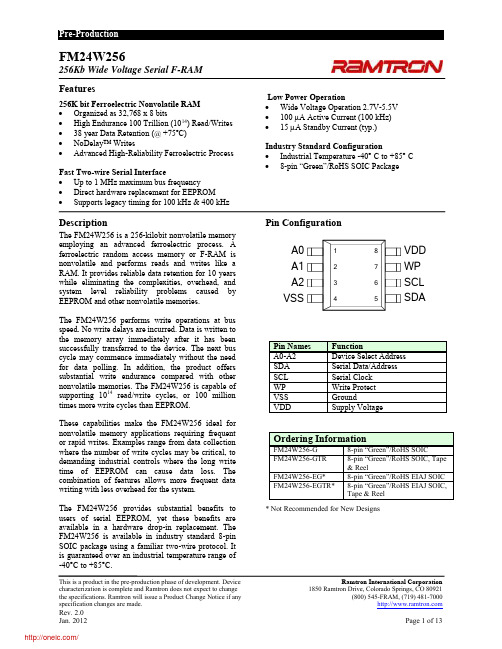
FM24W256 - 256Kb Wide Voltage I2C F-RAM
Counter
Address Latch
4,096 x 64 FRAM Array
8 SDA Serial to Parallel Converter
Description
The FM24W256 is a 256-kilobit nonvolatile memory employing an advanced ferroelectric process. A ferroelectric random access memory or F-RAM is nonvolatile and performs reads and writes like a RAM. It provides reliable data retention for 10 years while eliminating the complexities, overhead, and system level reliability problems caused by EEPROM and other nonvolatile memories. The FM24W256 performs write operations at bus speed. No write delays are incurred. Data is written to the memory array immediately after it has been successfully transferred to the device. The next bus cycle may commence immediately without the need for data polling. In addition, the product offers substantial write endurance compared with other nonvolatile memories. The FM24W256 is capable of supporting 1014 read/write cycles, or 100 million times more write cycles than EEPROM. These capabilities make the FM24W256 ideal for nonvolatile memory applications requiring frequent or rapid writes. Examples range from data collection where the number of write cycles may be critical, to demanding industrial controls where the long write time of EEPROM can cause data loss. The combination of features allows more frequent data writing with less overhead for the system. The FM24W256 provides substantial benefits to users of serial EEPROM, yet these benefits are available in a hardware drop-in replacement. The FM24W256 is available in industry standard 8-pin SOIC package using a familiar two-wire protocol. It is guaranteed over an industrial temperature range of -40°C to +85°C.
MEMORY存储芯片MT25QU256ABA1EW7-0SIT中文规格书

Serial NOR Flash Memory 1.8V , Multiple I/O, 4KB, 32KB, 64KB, Sector Erase MT25QU256ABAFeatures•SPI-compatible serial bus interface•Single and double transfer rate (STR/DTR)•Clock frequency –166 MHz (MAX) for all protocols in STR–90 MHz (MAX) for all protocols in DTR•Dual/quad I/O commands for increased through-put up to 90 MB/s•Supported protocols: Extended, Dual and Quad I/Oboth STR and DTR•Execute-in-place (XIP)•PROGRAM/ERASE SUSPEND operations•Volatile and nonvolatile configuration settings•Software reset•Additional reset pin for selected part numbers•3-byte and 4-byte address modes – enable memoryaccess beyond 128Mb•Dedicated 64-byte OTP area outside main memory–Readable and user-lockable–Permanent lock with PROGRAM OTP command•Erase capability–Bulk erase–Sector erase 64KB uniform granularity–Subsector erase 4KB, 32KB granularity•Erase performance: 400KB/sec (64KB sector)•Erase performance: 80KB/sec (4KB sub-sector)•Program performance: 2MB/sec•Security and write protection–Volatile and nonvolatile locking and softwarewrite protection for each 64KB sector–Nonvolatile configuration locking–Password protection–Hardware write protection: nonvolatile bits(BP[3:0] and TB) define protected area size–Program/erase protection during power-up–CRC detects accidental changes to raw data•Electronic signature–JEDEC-standard 3-byte signature (BB19h)–Extended device ID: two additional bytes identifydevice factory options•JESD47H-compliant–Minimum 100,000 ERASE cycles per sector–Data retention: 20 years (TYP)Options Marking •Voltage – 1.7-2.0V U •Density –256Mb 256•Device stacking –Monolithic A •Device generation B •Die revision A •Pin configuration –RESET# and HOLD#8•Sector size –64KB E •Packages – JEDEC-standard, RoHS-compliant –24-ball T-PBGA 05/6mm × 8mm (5 × 5 array)12–24-ball T-PBGA 05/6mm × 8mm (4 × 6 array)14–Wafer level chip-scale package, 23balls , 9 active balls (XFWLBGA 0.5P)55–16-pin SOP2, 300 mils (SO16W, SO16-Wide, SOIC-16)SF –W-PDFN-8 6mm × 5mm (MLP8 6mm × 5mm)W7–W-PDFN-8 8mm × 6mm (MLP8 8mm × 6mm)W9•Security features –Standard security 0•Special options –Standard S –Automotive A •Operating temperature range –From –40°C to +85°C IT –From –40°C to +105°C AT –From –40°C to +125°C UTCCMTD-1725822587-3458mt25q_qljs_U_256_ABA_xxT.pdf - Rev. K 07/18 EN 1 Technology, Inc. reserves the right to change products or specifications without notice. © 2014 Technology, Inc. All rights reserved.Products and specifications discussed herein are subject to change by without notice.Device DescriptionThe MT25Q is a high-performance multiple input/output serial Flash memory device. It features a high-speed SPI-compatible bus interface, execute-in-place (XIP) functionali-ty, advanced write protection mechanisms, and extended address access. Innovative,high-performance, dual and quad input/output commands enable double or quadru-ple the transfer bandwidth for READ and PROGRAM operations.Figure 2: Block DiagramNote: 1.Each page of memory can be individually programmed, but the device is not page-eras-able.256Mb, 1.8V Multiple I/O Serial Flash Memory Device DescriptionCCMTD-1725822587-3458mt25q_qljs_U_256_ABA_xxT.pdf - Rev. K 07/18 EN 9 Technology, Inc. reserves the right to change products or specifications without notice. © 2014 Technology, Inc. All rights reserved.Package Dimensions – Package Code: 12Figure 9: 24-Ball T -PBGA (5 x 5 ball grid array) – 6mm x 8mmNotes: 1.All dimensions are in millimeters.2.See Part Number Ordering Information for complete package names and details.256Mb, 1.8V Multiple I/O Serial Flash Memory Package Dimensions – Package Code: 12CCMTD-1725822587-3458mt25q_qljs_U_256_ABA_xxT.pdf - Rev. K 07/18 EN 18 Technology, Inc. reserves the right to change products or specifications without notice. © 2014 Technology, Inc. All rights reserved.Serial Flash Discovery Parameter DataThe serial Flash discovery parameter (SFDP) provides a standard, consistent method to describe serial Flash device functions and features using internal parameter tables. The parameter tables can be interrogated by host system software, enabling adjustments to accommodate divergent features from multiple vendors. The SFDP standard defines a common parameter table that describes important device characteristics and serial ac-cess methods used to read the parameter table data.Micron's SFDP table information aligns with JEDEC-standard JESD216 for serial Flash discoverable parameters. The latest JEDEC standard includes revision 1.6. Beginning week 42 (2014), Micron's MT25Q production parts will include SFDP data that aligns with revision 1.6.Refer to JEDEC-standard JESD216B for a complete overview of the SFDP table defini-tion.Data in the SFDP tables is read by the READ SERIAL FLASH DISCOVERY PARAMETER operation.See TN-25-06: Serial Flash Discovery Parameters for MT25Q Family for serial Flash discovery parameter data.256Mb, 1.8V Multiple I/O Serial Flash Memory Serial Flash Discovery Parameter DataCCMTD-1725822587-3458mt25q_qljs_U_256_ABA_xxT.pdf - Rev. K 07/18 EN 40 Technology, Inc. reserves the right to change products or specifications without notice. © 2014 Technology, Inc. All rights reserved.。
Vicor设计指南和应用手册(CHINESE)
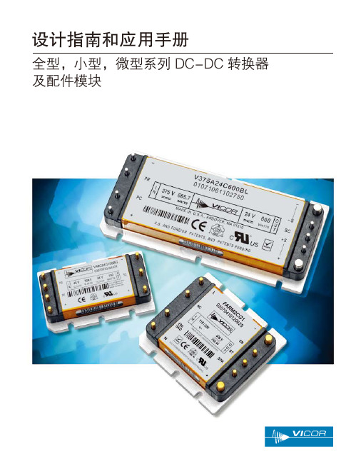
图 2-4 ─ PC / SC 模块警报时间
光耦合器
+IN
PC
4 kΩ PR
-IN
图 2-5 ─ 隔离导通指示器
+OUT
比较器
+IN
+S PC
SC
-S
警报
PR
-OUT
1.00V
–IN
+OUT SC
-OUT
比较器
1.00 V
警报
图 2-6-a ─ 次级导通状态(全型 / 小型模块)
图 2-6-b ─ 次级导通状态(微型模块)
全型、小型和微型系列 DC-DC 转换器及配件模块
全型、小型、微型系列的 DC-DC 转换器是 Vicor 以先 进的设计和制作程序来制造的模块;是公司整体元件功 率解决方案战略中的核心部分 (图 1-1)。该些模块齐备 多样且不受限的标准版本,以至于几乎分不清客制或标 准模块间的界限。
模块的控制器、电磁、开关和封装部件的独特设计,造 就了一个功率密度高达 120 W/in3 (7.3 W/cm3) 的元件, 有三种封装大小:
全型 4.6" x 2.2" x 0.5" (117 x 55.9 x 12.7 mm) 小型 2.28" x 2.2" x 0.5" (57.9 x 55.9 x 12.7 mm) 微型 2.28" x 1.45" x 0.5" (57.9 x 36.8 x 12.7 mm)
该些模块的元件数目只有其原先产品的三份之一。
2. 控制引脚功能及应用
初级控制(PC 引脚)
模块使能 / 失能 可通过将 PC 电压拉到 2.3 V 以下 (相 对于负输入),使模块失能(图 2-1)。这应该通过集电 极开路三极管、继电器或者光耦合器来实现。要使多个转 换器失能,可通过或门二极管配合一个三极管或者继电器 来实现。使用机械开关或者继电器控制 PC 引脚时,务必 使用电容配合(最大 10 nF),以免开关跳动。
MEMORY存储芯片MT25QU256ABA1EW7-0SIT中文规格书
Serial NOR Flash Memory 1.8V , Multiple I/O, 4KB, 32KB, 64KB, Sector Erase MT25QU256ABAFeatures•SPI-compatible serial bus interface•Single and double transfer rate (STR/DTR)•Clock frequency –166 MHz (MAX) for all protocols in STR–90 MHz (MAX) for all protocols in DTR•Dual/quad I/O commands for increased through-put up to 90 MB/s•Supported protocols: Extended, Dual and Quad I/Oboth STR and DTR•Execute-in-place (XIP)•PROGRAM/ERASE SUSPEND operations•Volatile and nonvolatile configuration settings•Software reset•Additional reset pin for selected part numbers•3-byte and 4-byte address modes – enable memoryaccess beyond 128Mb•Dedicated 64-byte OTP area outside main memory–Readable and user-lockable–Permanent lock with PROGRAM OTP command•Erase capability–Bulk erase–Sector erase 64KB uniform granularity–Subsector erase 4KB, 32KB granularity•Erase performance: 400KB/sec (64KB sector)•Erase performance: 80KB/sec (4KB sub-sector)•Program performance: 2MB/sec•Security and write protection–Volatile and nonvolatile locking and softwarewrite protection for each 64KB sector–Nonvolatile configuration locking–Password protection–Hardware write protection: nonvolatile bits(BP[3:0] and TB) define protected area size–Program/erase protection during power-up–CRC detects accidental changes to raw data•Electronic signature–JEDEC-standard 3-byte signature (BB19h)–Extended device ID: two additional bytes identifydevice factory options•JESD47H-compliant–Minimum 100,000 ERASE cycles per sector–Data retention: 20 years (TYP)Options Marking •Voltage – 1.7-2.0V U •Density –256Mb 256•Device stacking –Monolithic A •Device generation B •Die revision A •Pin configuration –RESET# and HOLD#8•Sector size –64KB E •Packages – JEDEC-standard, RoHS-compliant –24-ball T-PBGA 05/6mm × 8mm (5 × 5 array)12–24-ball T-PBGA 05/6mm × 8mm (4 × 6 array)14–Wafer level chip-scale package, 23balls , 9 active balls (XFWLBGA 0.5P)55–16-pin SOP2, 300 mils (SO16W, SO16-Wide, SOIC-16)SF –W-PDFN-8 6mm × 5mm (MLP8 6mm × 5mm)W7–W-PDFN-8 8mm × 6mm (MLP8 8mm × 6mm)W9•Security features –Standard security 0•Special options –Standard S –Automotive A •Operating temperature range –From –40°C to +85°C IT –From –40°C to +105°C AT –From –40°C to +125°C UTCCMTD-1725822587-3458mt25q_qljs_U_256_ABA_xxT.pdf - Rev. K 07/18 EN 1 Technology, Inc. reserves the right to change products or specifications without notice. © 2014 Technology, Inc. All rights reserved.Products and specifications discussed herein are subject to change by without notice.Device DescriptionThe MT25Q is a high-performance multiple input/output serial Flash memory device. It features a high-speed SPI-compatible bus interface, execute-in-place (XIP) functionali-ty, advanced write protection mechanisms, and extended address access. Innovative,high-performance, dual and quad input/output commands enable double or quadru-ple the transfer bandwidth for READ and PROGRAM operations.Figure 2: Block DiagramNote: 1.Each page of memory can be individually programmed, but the device is not page-eras-able.256Mb, 1.8V Multiple I/O Serial Flash Memory Device DescriptionCCMTD-1725822587-3458mt25q_qljs_U_256_ABA_xxT.pdf - Rev. K 07/18 EN 9 Technology, Inc. reserves the right to change products or specifications without notice. © 2014 Technology, Inc. All rights reserved.Package Dimensions – Package Code: 12Figure 9: 24-Ball T -PBGA (5 x 5 ball grid array) – 6mm x 8mmNotes: 1.All dimensions are in millimeters.2.See Part Number Ordering Information for complete package names and details.256Mb, 1.8V Multiple I/O Serial Flash Memory Package Dimensions – Package Code: 12CCMTD-1725822587-3458mt25q_qljs_U_256_ABA_xxT.pdf - Rev. K 07/18 EN 18 Technology, Inc. reserves the right to change products or specifications without notice. © 2014 Technology, Inc. All rights reserved.Serial Flash Discovery Parameter DataThe serial Flash discovery parameter (SFDP) provides a standard, consistent method to describe serial Flash device functions and features using internal parameter tables. The parameter tables can be interrogated by host system software, enabling adjustments to accommodate divergent features from multiple vendors. The SFDP standard defines a common parameter table that describes important device characteristics and serial ac-cess methods used to read the parameter table data.Micron's SFDP table information aligns with JEDEC-standard JESD216 for serial Flash discoverable parameters. The latest JEDEC standard includes revision 1.6. Beginning week 42 (2014), Micron's MT25Q production parts will include SFDP data that aligns with revision 1.6.Refer to JEDEC-standard JESD216B for a complete overview of the SFDP table defini-tion.Data in the SFDP tables is read by the READ SERIAL FLASH DISCOVERY PARAMETER operation.See TN-25-06: Serial Flash Discovery Parameters for MT25Q Family for serial Flash discovery parameter data.256Mb, 1.8V Multiple I/O Serial Flash Memory Serial Flash Discovery Parameter DataCCMTD-1725822587-3458mt25q_qljs_U_256_ABA_xxT.pdf - Rev. K 07/18 EN 40 Technology, Inc. reserves the right to change products or specifications without notice. © 2014 Technology, Inc. All rights reserved.。
JZ25-1S-SPC-MDR-CO-0003 REW 0
目录1 范围 (3)2内部对讲设备 (5)3电源要求 (8)4电缆 (8)5接地 (9)6备件 (9)7证书 (9)1 范围1.1概述本规格书涉及的内容,包含了JZ25-1南模块钻机内部对讲系统的最低技术要求。
本系统设备由厂家提供并用于JZ25-1南模块钻机。
1.2 参考依据:JZ25-1S-DWG-MDR-CO-0004内部对讲系统单线图1.3 标准与规范:所有设备的设计,材料和安装方法应符合下面的规范及要求。
• API RP 14F海上生产平台电气系统设计及安装推荐实施规程1999年9月4日版• API RP 500石油装置用电气设备位置分类推荐实施规程1997第二版• NFPA 70国际电气标准, 2002• IEC 60331-11,21,23,25电缆的防火特性 1999.4• IEC 60332 (1~3)电缆的燃烧试验 1989.3~2000.10• IEC 60945海上导航和无线电通信设备及系统一般要求 1996.11• 海上固定平台入级与建造规范 2000版• 中国民航总局:海上通讯设备规则• 全球海难安全系统 (GMDSS)• CCIR (国际无线电咨询委员会标准, ITU)• CCITT (国际电报电话咨询委员会标准 , ITU)1.4 定义与缩写DT 内部对讲话站SP 内部对讲扬声器CB 内部对讲闪光灯IE 阻抗均衡器IA 室内适配器DTJB 内部对讲接线箱批准类型:所有通讯设备类型必须符合中华人民共和国权威机构相关规定及要求。
1.5 详细设计:内部对讲系统的详细设计应在本规格书的具体要求下来完成,详细设计文件还应包括整个系统设备的外形。
1.5.1 采办在本项目具体运作期间,设备的发货,运输以及验货必须报批。
1.5.2 检测程序:厂家应提供一份关于设备检验以及相关海上调试的测试报告。
此报告将包含所有检测数据以及服务商在调试与完工时的工作内容。
此报告中的实验数据应以FAT(厂家调试验收)格式记录。
博磊达新能源科技有限公司产品规格书BLDB2R4025C-1说明书

1h 10min
可根据客户需求进 行设计
参考值
9 工作温度
充电 放电
-40°C ~ 45°C -40°C ~ 55°C
可根据客户需求进 行设计
10 贮存温度
短期(1 个月内) 长期(1 年内)
-40°C ~ 45°C -20°C ~ 20°C
11 储存湿度
<70﹪
12 电池重量
约 0.8kg
13 壳体材料
2 最小容量
25Ah@1C 放电
3 标称电压
2.3V
4 内阻
≤ 0.8mΩ
可根据客户需求进
充电(恒流恒压 最大充电电流
6C
5
行设计
CC-CV)
6 7 8
充电上限电压
2.7V
有限公司 放电
最大放电电流 放电终止电压
10C 1.5V
新能源科技 充电时间
标准充电 快速充电
磊达 推荐 SOC 使用窗 SOC :10%~90%
铝壳
2
产品规格书
版本号:A/0
产品规格书
型 号: BLDB2R4025C-1
1. 单体电池尺寸
博磊达新能源科技有限公司
项目 Φ H
描述 直径 高度(不含极柱)
尺寸 60mm ±0.5mm 138.3mm ±0.5mm
1
产品规格书
版本号:A/02.标称技术参数序号 Nhomakorabea项目
参数说明
备注
1 标称容量
25Ah@ 1C 放电
(参考资料)好利来保险丝1A 250V规格书
Hollyland (China) Electronics本规格书适用于本公司生产并获得CQC 、UR/CUR 、SEMKO 、PSE 、VDE 、BSI 、KC 认证的5ET RoHS 系列HOLLY 商标的超小型保险丝。
This specification defines the technical requirements of sub-miniature fuse type 5ET RoHS series with HOLLY ® 产品部件号为: brand, which are approved by CQC, UR/CUR, SEMKO, PSE, VDE 、BSI and KTL.型号 额定电流 额定电压 Construction of part no: type rated current rated voltage 5ET 0100 H A型号规格: 型号 特性符号 额定电流 MODEL DETAIL: 额定电压 Type Characteristic Symbol Rated Current 例如/ Example: Rated Voltage 5ET T 2 A *特性符号/ Characteristic Symbol: T – 慢断型/ Time-Lag.250V2. 相关标准及认证情况/ APPLICABLE STANDARDS & APPROVED DETAILS 2.1 5ET RoHS 系列产品适用的相关标准是 IEC 60127和GB 9364。
Applicable standards for 5ET RoHS series are IEC 60127 and GB 9364.Hollyland (China) Electronics3. 公司地址/ ADDRESS中国福建省厦门市湖里区枋湖路9-19号NO. 9-19, FANGHU ROAD, HULI, XIAMEN, FUJIAN, CHINA.4. 构造图/ CONSTRUCTION FIG . & DIMENSION4.2 方形塑料帽/ Square THERMOPLASTIC CAP 方形塑料帽无破裂、缺损或污染等现象。
ESM-2500产品规格书
※1
箱→(金
库)
※1
(1
角(2
(3Байду номын сангаас
))出循进环款款 hopper )备用零钱箱
中
没有
硬12币面面时值值。:: 2面值:
1 1
, 元,
元
55角角
(选
择)
1元,5角(选择)
循环 hopper
元 枚 1 : 700 角 枚 选择 5 :1000 ( )
备(用标准零钱1箱台)
元 枚 1 :700 角 枚 选择 5 :1000 ( )
: :
DC24V ±10%
消耗电流 外(形参尺照寸外形尺寸图)
重量
使用环境条件
・・・・外后整通保待工工( 工钱前不部方体常管机作作作但箱方包乱维环环对时时时5维含光护境平最境车0护钱:站均大0:箱:::从相相等m各拉保工约:投:对对建s出管作:::入2湿湿筑e部温温213583口.30度度物c4分度度.2.05.K0.0照Ak4范内范以g范范A9Ag㎜以㎜射以以围围内部围围以以(下(进下下程的下下W(W来()度冲)没的没×突的×-有33510有6灰电60℃0℃1填1%%0填2尘流2.充.tt0tt充3具,3oooo㎜硬㎜0硬有马88(币(5505币4一达%%50H时Hl℃时)℃定启)RR)HHx)×动耐×(对(6(时性679无工无6通等3..结作结4常高7㎜㎜露不露负峰(()会)荷电DD造)时流)成)除障外害)。
目录
概要 1.
····················································· 2
.适用 1-1
··················································· 2
MEMORY存储芯片MT25QL01GBBB8ESF-0SIT中文规格书
Features•Stacked device (two 512Mb die)•SPI-compatible serial bus interface•Single and double transfer rate (STR/DTR)•Clock frequency–133 MHz (MAX) for all protocols in STR –90 MHz (MAX) for all protocols in DTR•Dual/quad I/O commands for increased through-put up to 90 MB/s•Supported protocols: Extended, Dual and Quad I/O both STR and DTR •Execute-in-place (XIP)•PROGRAM/ERASE SUSPEND operations•Volatile and nonvolatile configuration settings •Software reset•Additional reset pin for selected part numbers•3-byte and 4-byte address modes – enable memory access beyond 128Mb•Dedicated 64-byte OTP area outside main memory –Readable and user-lockable •Erase capability –Die Erase–Sector erase 64KB uniform granularity –Subsector erase 4KB, 32KB granularity •Erase performance: 400KB/sec (64KB sector)•Erase performance: 80KB/sec (4KB sub-sector)•Program performance: 2MB/sec •Security and write protection–Volatile and nonvolatile locking and software write protection for each 64KB sector –Nonvolatile configuration locking –Password protection–Hardware write protection: nonvolatile bits (BP[3:0] and TB) define protected area size –Program/erase protection during power-up –CRC detects accidental changes to raw data •Electronic signature–JEDEC-standard 3-byte signature (BA21h)–Extended device ID: two additional bytes identify device factory options •JESD47H-compliant–Minimum 100,000 ERASE cycles per sector –Data retention: 20 years (TYP)OptionsMarking•Voltage – 2.7–3.6V L •Density –1Gb01G •Device stacking – 2 die stacked B •Device generation B •Die revisionB •Pin configuration –HOLD#1–RESET and HOLD#8•Sector Size –64KBE •Packages – JEDEC-standard, RoHS-compliant–24-ball T-PBGA 05/6mm x 8mm (TBGA24)12–16-pin SOP2, 300 mils (SO16W,SO16-Wide, SOIC-16)SF –W-PDFN-8 8mm x 6mm (MLP8 8mm x 6mm)W9•Security features –Standard security 0•Special options –Standard S –AutomotiveA •Operating temperature range –From –40°C to +85°C IT –From –40°C to +105°C AT –From –40°C to +125°CUT找Memory 、FPGA 、二三极管、连接器、模块、光耦、电容电阻、单片机、处理器、晶振、传感器、 滤波器,上深圳市美光存储技术有限公司Part Number OrderingMicron Serial NOR Flash devices are available in different configurations and densities. Verify valid part numbers by using Micron’s part catalog search at . To compare features and specifications by device type,visit /products. Contact the factory for devices not found.Figure 1: Part Number Ordering InformationProduction Status Blank = ProductionES = Engineering samples QS = Qualification samples Operating Temperature IT = –40°C to +85°C AT = –40°C to +105°C UT = –40°C to +125°CSpecial Options S = StandardA = Automotive grade AEC-Q100Security Features0 = Standard default securityPackage Codes12 = 24-ball T-PBGA, 05/6 x 8mm (5 x 5 array)14 = 24-ball T-PBGA, 05/6 x 8mm (4 x 6 array)SC = 8-pin SOP2, 150 mils SE = 8-pin SOP2, 208 mils SF = 16-pin SOP2, 300 mils W7 = 8-pin W-PDFN, 6 x 5mm W9 = 8-pin W-PDFN, 8 x 6mm 5x = WLCSP package 1Sector sizeE = 64KB sectors, 4KB and 32KB subsectorsMicron Technology Part Family 25Q = SPI NOR Voltage L = 2.7–3.6V U = 1.7–2.0V Density064 = 64Mb (8MB)128 = 128Mb (16MB)256 = 256Mb (32MB)512 = 512Mb (64MB)01G = 1Gb (128MB)02G = 2Gb (256MB)StackA = 1 die/1 S#B = 2 die/1 S#C = 4 die/1 S#Device Generation B = 2nd generation Die Revision A = Rev. A B = Rev. BPin Configuration Option 1 = HOLD# pin 3 = RESET# pin8 = RESET# and HOLD# pinMT 25Q LxxxA BA1ESF IT-SESNote: 1.WLCSP package codes, package size, and availability are density-specific. Contact the factory for availability.Device DescriptionThe MT25Q is a high-performance multiple input/output serial Flash memory device. Itfeatures a high-speed SPI-compatible bus interface, execute-in-place (XIP) functionali-ty, advanced write protection mechanisms, and extended address access. Innovative,high-performance, dual and quad input/output commands enable double or quadru-ple the transfer bandwidth for READ and PROGRAM operations.Figure 2: Block DiagramNote: 1.Each page of memory can be individually programmed, but the device is not page-eras-able.1Gb, 3V Multiple I/O Serial Flash MemoryMemory Map – 1Gb Density1Gb, 3V Multiple I/O Serial Flash MemoryStatus Register Status RegisterStatus register bits can be read from or written to using READ STATUS REGISTER orWRITE STATUS REGISTER commands, respectively. When the status register enable/disable bit (bit 7) is set to 1 and W# is driven LOW, the status register nonvolatile bitsbecome read-only and the WRITE STATUS REGISTER operation will not execute. Theonly way to exit this hardware-protected mode is to drive W# HIGH.。
DTS6400规格书(最新版)
1N-Channel 60-V (D-S) MOSFETFEATURES•Halogen-free According to IEC 61249-2-21Available•TrenchFET ® Power MOSFET •100 % R g Tested •100 % UIS TestedAPPLICATIONS•Battery Switch •DC/DC ConverterPRODUCT SUMMARYV DS (V)R DS(on) (Ω)I D (A)aQ g (Typ.)600.026 at V GS = 10 V 4.5 2.3 nC0.036 at V GS = 4.5 V2.1GSDTop V ie wTO-236Notes: a.Based on T C = 25 °C.b.Surface Mounted on 1" x 1" FR4 board.c.t = 5 s.d.Maximum under Steady State conditions is 130 °C/W.ABSOLUTE MAXIMUM RATINGS T A = 25 °C, unless otherwise notedParameterSymbol Limit Unit Drain-Source Voltage V DS 60VGate-Source VoltageV GS± 20Continuous Drain Current (T J = 150 °C)T C = 25 °C I D 4.5AT C = 70 °C 1.8T A = 25 °C 2.9b, c T A = 70 °C1.5b, c Pulsed Drain CurrentI DM 8Continuous Source-Drain Diode Current T C = 25 °C I S 1.39T A = 25 °C 0.91b, cAvalanche CurrentL = 0.1 mH I AS 6Single-Pulse Avalanche Energy E AS 1.8mJ Maximum Power DissipationT C = 25 °C P D 1.66W T C = 70 °C 1.06T A = 25 °C 1.09b, c T A = 70 °C 0.7b, c Operating Junction and Storage T emperature RangeT J , T stg- 55 to 150°CTHERMAL RESISTANCE RATINGSParameterSymbol Typical Maximum Unit Maximum Junction-to-Ambient b, d≤ 5 s R thJA 90115°C/WMaximum Junction-to-Foot (Drain)Steady State R thJF607523553Q68872黄R1376032电50702Notes:a.Pulse test; pulse width ≤ 300 µs, duty cycle ≤ 2 %.b.Guaranteed by design, not subject to production testing.Stresses beyond those listed under “Absolute Maximum Ratings” may cause permanent damage to the device. These are stress ratings only, and functional operation of the device at these or any other conditions beyond those indicated in the operational sections of the specifications is not implied. Exposure to absolute maximum rating conditions for extended periods may affect device reliability.MOSFET SPECIFICATIONS T J = 25 °C, unless otherwise notedParameter SymbolTest Conditions Min.Typ.Max.UnitStaticDrain-Source Breakdown Voltage V DS V DS = 0 V , I D = 250 µA60V V DS Temperature Coefficient ΔV DS /T J I D = 250 µA 55mV/°C V GS(th) T emperature Coefficient ΔV GS(th)/T J - 5Gate-Source Threshold Voltage V GS(th) V DS = V GS , I D = 250 µA 13V Gate-Source LeakageI GSS V DS = 0 V, V GS = ± 20 V ± 100nA Zero Gate Voltage Drain Current I DSS V DS = 60 V , V GS = 0 V 1µA V DS = 60 V, V GS = 0 V , T J = 55 °C10On-State Drain Current aI D(on)V DS ≥ 5 V, V GS = 10 V 8A Drain-Source On-State Resistance a R DS(on)V GS = 10 V , I D = 1.9 A 0.0190.026ΩV GS = 4.5 V , I D = 1.7 A 0.0260.036Forward T ransconductance a g fsV DS = 15V , I D = 1.9 A5SDynamic bInput Capacitance C iss V DS = 30 V , V GS = 0 V , f = 1 MHz 190pFOutput CapacitanceC oss 26Reverse Transfer Capacitance C rss 15Total Gate Charge Q g V DS = 30 V , V GS = 10 V , ID = 1.9 A 4.5 6.8nC V DS = 30 V, V GS = 4.5 V, I D = 1.9 A2.33.5Gate-Source Charge Q gs 0.8Gate-Drain Charge Q gd 1Gate Resistance R g f = 1 MHz0.62.8 5.6ΩTurn-On Delay Time t d(on) V DD = 30 V, R L = 20 ΩI D ≅ 1.5 A, V GEN = 10 V , R G = 1 Ω46ns Rise Timet r 1015Turn-Off Delay Time t d(off) 1015Fall Timet f 710.5Turn-On Delay Time t d(on) V DD = 30 V, R L = 20 ΩI D = 1.5 A, V GEN = 4.5 V , R G = 1 Ω1523ns Rise Timet r 1624Turn-Off Delay Time t d(off) 1117Fall Timet f1117Drain-Source Body Diode Characteristics Continuous Source-Drain Diode Current I S T C = 25 °C2.39A Pulse Diode Forward Current a I SM 8Body Diode VoltageV SD I S = 1.5 A0.8 1.2V Body Diode Reverse Recovery Time t rr I F = 1.5 A, dI/dt = 100 A/µs, T J = 25 °C1523ns Body Diode Reverse Recovery Charge Q rr 1015nC Reverse Recovery Fall Time t a 12nsReverse Recovery Rise Timet b3Output Characteristics Transfer CharacteristicsOn-Resistance vs. Junction Temperature3Threshold Voltage Single Pulse PowerSafe Operating Area45TYPICAL CHARACTERISTICS 25°C, unless otherwise noted*The power dissipation P D is based on T J(max.) = 150 °C, using junction-to-case thermal resistance, and is more useful in settling the upper dissipation limit for cases where additional heatsinking is used. It is used to determine the current rating, when this rating falls below the package limit.Current Derating*Power Derating, Junction-to-CasePower Derating, Junction-to-Ambient.Normalized Thermal Transient Impedance, Junction-to-AmbientNormalized Thermal Transient Impedance, Junction-to-Foot THERMAL RATINGS (T A = 25 °C, unless otherwise noted)61SOT-23 (TO-236): 3-LEADDimMILLIMETERS INCHESMinMaxMinMaxA 0.89 1.120.0350.044A 10.010.100.00040.004A 20.88 1.020.03460.040b 0.350.500.0140.020c0.0850.180.0030.007D 2.803.040.1100.120E 2.10 2.640.0830.104E 1 1.201.400.0470.055e 0.95 BSC 0.0374 Ref e 1 1.90 BSC0.0748 RefL 0.400.600.0160.024L 10.64 Ref 0.025 Ref S 0.50 Ref0.020 Refq3°8°3°8°ECN: S-03946-Rev. K, 09-Jul-01DWG: 54791A P P L I C A T I O N N O T ERECOMMENDED MINIMUM PADS FOR SOT-23。
- 1、下载文档前请自行甄别文档内容的完整性,平台不提供额外的编辑、内容补充、找答案等附加服务。
- 2、"仅部分预览"的文档,不可在线预览部分如存在完整性等问题,可反馈申请退款(可完整预览的文档不适用该条件!)。
- 3、如文档侵犯您的权益,请联系客服反馈,我们会尽快为您处理(人工客服工作时间:9:00-18:30)。
规格承认书 Specification for approval
产品名称:5.250/BTC系列 慢断型 陶瓷管保险丝 Product Type: 5.250/BTC Series Time-Lag Ceramic Tube Fuse
Version No.:2013001
Reomax Electronics (HK) Limited Add: 5th Floor, Bright way tower, No.33 Mong kok road, Kowloon Hong Kong Web: http://www.reomaxfuse.net
Spec. No.: SFA-5.250BTC Reomax Electronics Co., LTD © 2013 Reomax Electronics Specifications are subject to change without notice Revised: 01/25/13
5.250/BTC系列产品规格书 5.250/BTC Series Specification
2 目录Contents
1. 适用范围 / Scope of Application ......................................................................................................................... 3 2. 安规认证标准及编号 / Standards and Agency Approvals ................................................................................. 3 3. 产品标示 / Product Marking ............................................................................................................................... 4 4. 外观及形状 / Appearances and Configuration ................................................................................................... 5 5. 结构及尺寸 / Dimensions and Structure ............................................................................................................ 5 6. 材料明细 / Material Details ................................................................................................................................ 6 7. 产品特性 / Product Characteristics .................................................................................................................... 6 8. 电气特性 / Electrical Characteristics .................................................................................................................. 6 9. 环境特性 / Environmental Characteristic ........................................................................................................... 8 10. 安装建议 / Installation Recommendations ........................................................................................................ 9 11. 包装 / Packaging ................................................................................................................................................ 10 12. 其他 / Others ..................................................................................................................................................... 11 附件I: 安规证书 / Appendix I: Safety approval certificates ................................................................................... 11 © 2013 Reomax Electronics Specifications are subject to change without notice Revised: 01/25/13
5.250/BTC系列产品规格书 5.250/BTC Series Specification
3 1. 适用范围 / Scope of Application 本产品适用于各类电子设备电路的过流保护作用, 广泛应用于照明设备、电源设备以及适配器等领域。This product is suitable for various kinds of electronic devices’ circuit over current protection. Widely used in industrial of Lighting, Power supply and Adapter applications, etc.
2. 安规认证标准及编号 / Standards and Agency Approvals 2.1执行标准:遵循UL 248 -1 / -14。 Standards:In accordance with UL 248 -1 / -14.
2.2认证范围 Certification: 额定电压 Voltage Rating 安规标准 Agency 认证范围 Ampere Range 证书编号 Agency File Number
125V/250V UL 200mA ~ 30A E340427(JDYX) C-UL 200mA ~ 30A E340427( JDYX7) PSE 200mA ~ 10A Pending
KTL 200mA ~ 10A Pending
2.3 目录编号 Catalogue No.,A = 250V/ B =125V,● Approved / ○ Pending 目录编号 Catalog No. 额定电流 Ampere Rating 额定电压 Voltage Rating 分断能力 Breaking Capacity 熔化热能 I2TMelting Integral(A2.S)
安规认证 Agency Approvals
BTC0100A/B 100mA 250V/125V 10000A@125 V AC (200mA~10A); 35A@250V AC (200mA~1A); 100A@250V AC 0.002 ○ ○ ○ BTC0125A/B 125mA 250V/125V 0.003 ○ ○ ○ BTC0160A/B 160mA 250V/125V 0.005 ○ ○ ○ BTC0200A/B 200mA 250V/125V 0.01 ● ● ○ BTC0250A/B 250mA 250V/125V 0.02 ● ● ○ BTC0300A/B 300mA 250V/125V 0.04 ● ● ○ BTC0315A/B 315mA 250V/125V 0.045 ● ● ○ BTC0350A/B 350mA 250V/125V 0.055 ● ● ○ BTC0400A/B 400mA 250V/125V 0.07 ● ● ○ © 2013 Reomax Electronics Specifications are subject to change without notice Revised: 01/25/13
5.250/BTC系列产品规格书 5.250/BTC Series Specification
4 BTC0500A/B 500mA 250V/125V (1.25A~3.5A); 200A@250V AC (4A~10A). 0.1 ● ● ○ BTC0600A/B 600mA 250V/125V 0.11 ● ● ○ BTC0630A/B 630mA 250V/125V 0.2 ● ● ○ BTC0750A/B 750mA 250V/125V 0.35 ● ● ○ BTC0800A/B 800mA 250V/125V 0.45 ● ● ○ BTC1100A/B 1A 250V/125V 0.9 ● ● ○ BTC1125A/B 1.25A 250V/125V 1.3 ● ● ○ BTC1150A/B 1.5A 250V/125V 1.6 ● ● ○ BTC1160A/B 1.6A 250V/125V 2.5 ● ● ○ BTC1200A/B 2A 250V/125V 5.8 ● ● ○ BTC1250A/B 2.5A 250V/125V 7.6 ● ● ○ BTC1300A/B 3A 250V/125V 8.1 ● ● ○ BTC1315A/B 3.15A 250V/125V 11 ● ● ○ BTC1350A/B 3.5A 250V/125V 19 ● ● ○ BTC1400A/B 4A 250V/125V 28 ● ● ○ BTC1500A/B 5A 250V/125V 40 ● ● ○ BTC1600A/B 6A 250V/125V 50 ● ● ○ BTC1630A/B 6.3A 250V/125V 64 ● ● ○ BTC1700A/B 7A 250V/125V 107 ● ● ○ BTC1800A/B 8A 250V/125V 133 ● ● ○ BTC2100A/B 10A 250V/125V 242 ● ● ○ 5.250.2150A/B 15A 250V/125V 368 ● ● ○ 5.250.2200A/B 20A 250V/125V 442 ● ● ○ 5.250.2250A/B 25A 250V/125V 568 ● ● ○ 5.250.2300A/B 30A 250V/125V 715 ● ● ○