Fabrication of 3D-photonic crystals via UV-nanoimprint lithography
LHM教程 - (1)
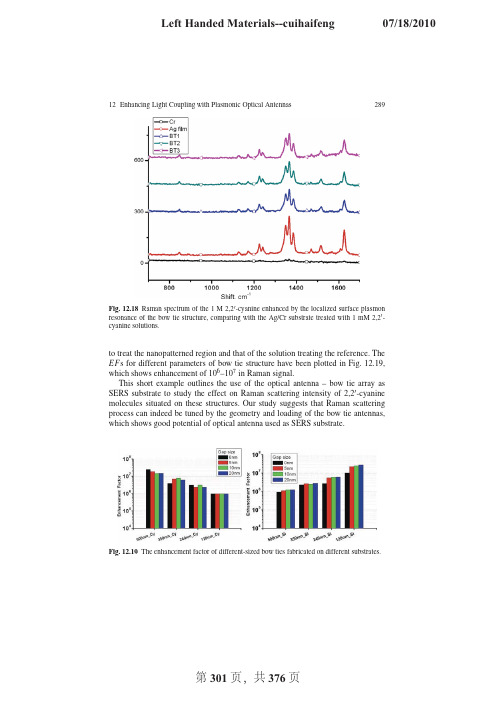
12Enhancing Light Coupling with Plasmonic Optical Antennas289Fig.12.18Raman spectrum of the1M2,2 -cyanine enhanced by the localized surface plasmon resonance of the bow tie structure,comparing with the Ag/Cr substrate treated with1mM2,2 -cyanine solutions.to treat the nanopatterned region and that of the solution treating the reference.The EF s for different parameters of bow tie structure have been plotted in Fig.12.19, which shows enhancement of106–107in Raman signal.This short example outlines the use of the optical antenna–bow tie array as SERS substrate to study the effect on Raman scattering intensity of2,2 -cyanine molecules situated on these structures.Our study suggests that Raman scattering process can indeed be tuned by the geometry and loading of the bow tie antennas, which shows good potential of optical antenna used as SERS substrate.Fig.12.19The enhancement factor of different-sized bow ties fabricated on different substrates.290Jun Xu,Anil Kumar,Pratik Chaturvedi,Keng H.Hsu and Nicholas X.Fang 12.5SummaryHarvesting and confining light using plasmonic nanoantennas represent an interest-ing frontier of metamaterial research.The convergence of RF and optical device designs will bring revolutionary changes in highly compact and integrated pho-tonics for photon energy conversion,adaptive sensing,and image processing.We expect many inspirations from RF metamaterial research to be transformed on the study of optical antennas and this could bring a profound impact to thefield of nanophotonics.Acknowledgments The authors are grateful for thefinancial supports from the Defense Advanced Research Projects Agency(grant HR0011-05-3-0002),Office of Naval Research(grant N00173-07-G013),and National Science Foundation(grant CMMI-0709023).Cathodoluminescence ex-periments were carried out in the Frederick Seitz Materials Research Laboratory Central Facilities, University of Illinois,which are partially supported by the U.S.Department of Energy under grants DE-FG02-07ER46453and DE-FG02-07ER46471.References1.Alu,A.,and Engheta,N.:Tuning the scattering response of optical nanoantennas with nanocir-cuit loads.Nat.Photon.2,307–310(2008)2.Alu,A.,and Engheta,N.:Input impedance,nanocircuit loading and radiation tuning of opticalnanoantennas.Phys.Rev.Lett.101,043901–043904(2008)3.Aroca,R.:Surface-enhanced Vibrational John Wiley&Sons Ltd,Chich-ester(2006)4.Bharadwaj,P.,and Novotny,L.:Spectral dependence of single moleculefluorescence enhance-ment.Opt.Express15,14266–14274(2007)5.Bohren,C.F.,and Huffman,D.R.:Absorption and Scattering of Light by Small Particles.Wiley,New York(1998)6.Bryant,G.W.,Abajo,F.J.G.,and Aizpurua,J.:Mapping the plasmon resonances of metallicnanoantennas.Nano Lett.8,631–636(2008)7.Chou,S.Y.,Krauss,P.R.,and Renstrom,P.J.:Nanoimprint lithography.J.Vac.Sci.Technol.B14,4129–4133(1996)8.Chou,S.Y.,Krauss,P.R.,Zhang,W.,Guo,L.,and Zhuang,L.:Sub-10nm imprint lithographyand applications.J.Vac.Sci.Technol.B15,2897–2904(1997)9.Crozier,K.B.,Sundaramurthy,A.,Kino,G.S.,and Quate,C.F.:Optical antennas:resonatorsfor localfield enhancement.J.Appl.Phys.94,4632–4642(2003)10.Cubukcu,E.,Kort,E.A.,Crozier,K.B.,and Cappaso,F.:Plasmonic laser antenna.Appl.Phys.Lett.89,093120–093123(2006)11.Draine,B.T.,and Flatau,P.J.:User guide for the Discrete Dipole Approximation CodeDDSCAT7.0./abs/0809.033712.Engheta,N.,Salandrino,A.,and Alu,A.:Circuit elements at optical frequencies:Nanoinduc-tors,nanocapacitors and nanoresistors.Phys.Rev.Lett.95,095504.4(2005)13.Farahani,J.N.,Eisler,H.J.,Pohl,D.W.,Pavius,M.,Fluckiger,P.,Gasser,P.,and Hecht,B.:Bow-tie optical antenna probes for single-emitter scanning near-field optical microscopy.Nan-otechnology18,125506(2007)14.Fleischmann,M.,Hendra,P.J.,and McQuillan,A.J.:Raman spectra of pyridine ad-sorbed ata silver electrode.Chem.Phys.Lett.26,163–166(1974)12Enhancing Light Coupling with Plasmonic Optical Antennas291 15.Fromm,D.P.,Sundaramurthy,A.,Schuck,P.J.,Kino,G.,and Moerner,W.E.:Gap-dependentoptical coupling of single bowtie nanoantennas resonant in the visible.Nano Lett.4,957–961 (2005)16.Garcia de Abajo,F.J.,and Howie,A.:Relativistic electron energy loss and electron-inducedphoton emission in inhomogeneous dielectrics.Phys.Rev.Lett.80,5180(1998)17.Garcia de Abajo,F.J.,and Kociak,M.:Probing the photonic local density of states with elec-tron energy loss spectroscopy.Phys.Rev.Lett.100,106804.4(2008)18.Grant,A.M.,and Creighton,J.A.:Anomalously intense Raman spectra of pyridine at a silverelectrode.J.Am.Chem.Soc.99,5215–5219(1977)19.Haes,A.J.,Haynes,C.L.,McFarland,A.D.,Schatz,G.C.,Van Duyne,R.R.,and Zou,S.L.:Plasmonic materials for surface-enhanced sensing and spectroscopy.MRS Bull.30,368–375 (2005)20.Hao,E.,and Schatz,G.C.:Electromagneticfields around silver nanoparticles and dimers.J.Chem.Phys.120,357–366(2004)21.Hewageegana,P.,and Stockman,M.I.:Plasmonic enhancing nanoantennas for photodetection.Infrared Phys.Tech.50,177–181(2007)22.Hsu,K.H.,Schultz,P.L.,Ferreira,P.M.,and Fang,N.X.:Electrochemical nanoim-printingwith solid-state superionic stamps.Nano Lett.7,446–451(2007)23.Ishi,T.,Fujikata,J.,Makita,K.,Baba,T.,and Ohashi,K.:Si nano-photodiode with a surfaceplasmon antenna.Japan.J.Appl.Phys.44,L364–L366(2005)24.Jeanmaire,D.L.,and Van Duyne,R.P.:Surface Raman electrochemistry part I.Heterocyclic,aromatic and aliphatic amines adsorbed on the anodized silver electrode.J.Electro Anal.Chem.84,1–20(1977)25.Kempa,K.,Rybczynski,J.,Huang,Z.,Gregorczyk,K.,Vidan,A.,Kimball,B.,Carl-son,J.,Benham,G.,Wang,Y.,Herczynski,A.,and Ren,Z.:Carbon nanotubes as optical antennae.Adv.Mater.19,421–426(2007)26.Kim,S.,Jin,J.H.,Kim,Y.J.,Park,I.Y.,Kim,Y.,and Kim,S.W.:High-harmonic gen-erationby resonant plasmonfield enhancement.Nature453,757–760(2008)27.M¨u hlschlegel,P.,Eisler,H.-J.,Martin,O.J.F.,Hecht,B.,and Pohl,D.W.:Resonant opticalantennas.Science308,1607–1609(2005)28.Mock,J.J.:Shape effects in plasmon resonance of individual colloidal silver nanopar-ticles.J.Chem.Phys.116,6755(2002)29.Novotny,L.:Effective wavelength scaling for optical antennas.Phys.Rev.Lett.98,266802–266804(2007)30.Palik,E.D.:Handbook of Optical Constants of Solids.Academic Press,Orlando,FL(1984)31.Schuck,P.J.,Fromm,D.P.,Sundaramurthy,A.,Kino,G.S.,and Moerner,W.E.:Im-provingthe mismatch between light and nanoscale objects with gold bowtie nanoantennas.Phys.Rev.Lett.94,017402–017404(2005)32.Schultz,P.L.,Hsu,K.H.,Fang,N.X.,and Ferreira,P.M.:Solid-state electrochemical nanoim-printing of copper.J.Vac.Sci.Technol.B25,2419–2424(2007)33.Shumaker-Parry,J.S.,Rochholz,H.,and Kreiter,M.:Fabrication of crescent-shaped opticalantennas.Adv.Mater.17,2131–2134(2005)34.Sivenpiper,D.et al.:High-impedance EM surfaces with a forbidden frequency band.IEEETrans.Micro.Theo.Tech.47,2059(1999)35.Tang,L.,and Miller,D.A.B.:C-shaped nanoaperture-enhanced Germanium photodetector.Opt.Lett.31,1519–1521(2006)36.Wang,Y.,Kempa,K.,Kimball,B.,Carlson J.B.,Benham,G.,Li,W.Z.,Kempa,T.,Rybczyn-ski,J.,Herczynski,A.,and Ren,Z.F.:Receiving and transmitting light-like ra-diowaves: antenna effect in arrays of aligned carbon nanotubes.Appl.Phys.Lett.85,2607–2609(2004)Chapter13Wideband and Low-Loss Metamaterialsfor Microwave and RF Applications:Fast Algorithm and Antenna DesignLe-Wei Li,Ya-Nan Li and Li HuAbstract In this chapter,a fast solver,i.e.,adaptive integral method(AIM)which is based on hybrid volume–surface integral equation,is utilized in the numerical sim-ulation of electromagnetic scattering from composite left-handed materials(LHM) such as split-ring resonators(SRR)with rods/wires.The volume electricfield inte-gral equation(EFIE)is applied to the dielectric region of this LHM,and the surface EFIE is applied on the conducting surface.The method of moments(MoM)is used to discretize the integral equation into a matrix solution and AIM is employed to reduce the memory requirement and CPU time for the matrix solution.Numeri-cal results and computational complexity analysis have shown that the AIM solver can significantly reduce the computational cost while maintaining a good accuracy. Inspired by the periodicity of SRR,the ASED-AIM,a new adaptive integral ap-proach based on accurate sub-entire-domain method,has been proposed to solve the electromagnetic scattering by large-scalefinite periodic arrays,especially the LHM structures like SRR.Several results are shown to demonstrate the efficiency of the method in solving periodic structures.Additionally,further computational time saving scheme for calculating the near-zone interaction matrix has been pro-posed.Both2-D and3-D periodic structures can be solved by this fast solver with impressive efficiency and accuracy.In the last section of this chapter,a novel rect-angular patch antenna was specifically designed using planar-patterned LHM con-cepts.This new antenna has demonstrated to have left-handed characteristics.It is shown to have great impact on the antenna performance enhancement in terms of the bandwidth significantly broadened and also in terms of high efficiency,low loss,and low VSWR.A good agreement is achieved between the simulation and measured results.This new antenna designed has strong radiation in the horizontal direction within the entire working band,which is desirable for some special applications. Joshua Le-Wei Li∗,Ya-Nan Li and Li HuDepartment of Electrical and Computer Engineering,National University of Singapore,10Kent Ridge Crescent,Singapore119260.∗e-mail:lwli@.sgT.J.Cui et al.(eds.),Metamaterials,DOI10.1007/978-1-4419-0573-413,293 c Springer Science+Business Media,LLC2010294Le-Wei Li,Ya-Nan Li and Li Hu Key words:Method of moments,split-ring resonator,adaptive integral method, electricfield integral equations,hybrid volume surface integral equations,ASED-AIM,finite periodical structure,scattering,RCS,LHM antenna,wideband,high gain,horizontal radiation,planar LHM,RF application.13.1Adaptive Integral Method(AIM)for Left-Handed Material(LHM)SimulationLeft-handed material(LHM)[43],which is also known as negative index material (NIM),represents a material of simultaneous negative permeability and permittivity. Typical LHMs,such as split-ring resonator(SRR)structure[41],are composed of a large array of periodical elements of dielectric body and conducting patches which usually require considerable computational costs during numerical simulation.Pre-vious researchers have often used the method of moments(MoM)[18]to carry out numerical simulations and have proven its reliability and accuracy.Among sev-eral fast solvers which are developed based on MoM,the adaptive integral method (AIM)[3,23,13]is one of the very efficient solvers which can tremendously reduce the memory requirement for LHM structures like SRR and accelerate the matrix-vector multiplications in the iterative solution procedure.13.1.1Hybrid Volume–Surface Integral Equation(VSIE)andMoM for SRRsFor SRR structures,both the dielectric substrate and the metal layer have induced currents and therefore contribute to scatteredfield to the total electromagnetic(EM)field.So,we need to adopt hybrid volume–surface integral equations(VSIE)to characterize thefield.In the dielectric region V,by taking the scatteredfield from both the surface current and the volume current into consideration,the total electricfield becomesE(r)=E i(r)+E s V(r)+E s S(r),r∈V,(13.1) where E(r)represents the totalfield in region V,E i(r)denotes the incidentfield, while E s V(r)and E s S(r)stand for the electricfields scattered by volume elements and surface elements in region V,respectively.Since the SRR structure consists of a very thin metal layer and dielectric body where the thickness of the metal layer can be considered to be almost0,the tangen-tial components of total electricfield vanishes on conducting surface:n×E i(r)=− n×E s V(r)− n×E s S(r).(13.2)13Antenna Design Using Metamaterials and Fast Solver295Equations(13.1)and(13.2)are known as the electricfield integral equations (EFIE)as they involve only electricfield.The EFIE is suitable for structures with open conducting surface.Inside the dielectric region V and on the surface S of con-ducting body,the incident wave induces a volume current J V and a surface current J S.The induced volume and surface currents can generate scattered electromagnetic field as follows:E sΩ(r)=−jk0η0AΩ(r)−∇ΦΩ(r),Ω=S or V,(13.3) where the magnetic vector potential is defined asAΩ(r)=ΩJΩ(r,r )g(r,r )d r ,Ω=S or V,(13.4)while the electric scalar potential is defined asΦΩ(r)=−η0jk0Ω∇ ·JΩ(r,r )g(r,r )d r ,Ω=S or V,(13.5)where g(r,r )=e−jk0|r−r |4π|r−r |,η0=μ0ε0,and k0denotes the wave number of back-ground medium(free space in this SRR investigation).The volume of dielectric material and surface of conducting body of SRR are meshed into tetrahedral elements and triangular patches,respectively.These basis function elements are used because of theirflexibility to model arbitrarily shaped3-D objects.The volume and surface currents are expanded using different vector basis functions.For surface elements,it is convenient to use the planar triangular basis functions or the Rao–Wilton–Glisson(RWG)basis functions[37]to expand the equivalent surface electric current.As for volume elements,similarly,we can apply the Schaubert–Wilton–Glisson(SWG)basis functions[39]to expand the equivalent volume electric current,that is,J S=N S∑n=1I S n f S n,(13.6a)J V=jωN V∑n=1˜ε(r)−ε0˜ε(r)I V n f V n=jωN V∑n=1κ(r)I V n f V n,(13.6b)whereκ(r)=˜ε(r)−ε0(r)denotes the contrast ratio and˜ε(r)represents the perme-ability of a tetrahedron element.After substituting above equations into the EFIE,we apply the Galerkin’s MoM testing procedure.Then,the integral equations are converted into a linear equationsystem written as¯Z VV¯Z V S¯Z SV¯Z SSI VI S=E VE S,(13.7)296Le-Wei Li,Ya-Nan Li and Li Hu where the vectors I V and I S represent the expansion coefficients of volume currents and surface currents,respectively.The excitation vector can be computed usingE V m=V mf V m·E i(r )d r ,(13.8a)E S m=S mf S m·E i(r )d r .(13.8b)The elements of the block matrices in Eq.(13.7)can be computed using the formulas shown below:Z VV mn=V mf V m f V n˜εd r−ωk bηbV mf V mV nκf V n g(r,r )d r +∇k2bV n∇ ·κf V ng(r,r )d r,(13.9a)Z V S mn=jk bηbV mf V m·S nf s n g(r,r )d r +∇k2bS n∇ ·f S n g(r,r )d rd r,(13.9b)Z SV mn=−ωk bηbS mf S m·V nκf V n g(r,r )d r +∇k2bV n∇ ·κf V ng(r,r )d rd r,(13.9c)Z SS mn=jk bηbS mf S m·S nf S n g(r,r )d r +∇k2bS n∇ ·f S n g(r,r )d rd r,(13.9d)whereκdenotes a constant value within the tetrahedron and can be taken out fromthe integration:∇·κf V n=κ∇·f V n+∇κ·f V n.(13.10)The second term given by the above equation in(13.10)is∇κ·f V n=I V n(κ+n−κ−n),on the common face t;0,elsewhere.(13.11)13.1.2Formulations for AIMThe matrix-vector multiplication implemented inside the AIM solution procedure can be summarized using the following four steps[14]:•to project the sources distributed on the basis functions onto the regular grid by matching their vector and scalar potentials at some given test points to guarantee the approximate equality of their farfields;•to evaluate the potentials at other grid locations produced by these grid-projected sources by a3-D convolution;•to interpolate the grid point potentials onto the testing functions;the projec-tion and interpolation operators are represented by sparse matrices,and the13Antenna Design Using Metamaterials and Fast Solver297 convolution can be carried out rapidly using discrete fast Fourier transforms (FFTs);and•to compute the near-field interactions directly and remove the errors introduced by the far-field operators.To employ the AIM,the object is enclosed in a rectangular grid and then re-cursively subdivided into small rectangular grids.In order to use the FFT to ap-proximate the far-zone interaction,we need to transfer the SWG and RWG basis functions into the Cartesian grids.It is noted that by using vector identity and di-vergence theorem,the∇operator in Eq.(13.9a)can be shifted and operated on the testing functions[37,39].Hence,we can denoteγn to represent any one of the com-ponents{f S,κf V,∇·(κf V)}and express all the matrix elements in Eq.(13.9a)in the following unified form:Z mn=αmαnγm(r)g(r,r )γn(r )d r d r.(13.12)The transformation functionγn(r)can be approximated as a linear combination of Dirac delta functions,i.e.,γn(r)≈ˆγ(r)=(m+1)3∑u=1Λnuδ(r−r ),(13.13)where m represents the expansion order,whileΛnu denotes the expansion coeffi-cients ofγn(r)and it can be determined using the multipole expansion or far-field approximation[23].The multipole expansion method is applied based on the crite-rion that the coefficientsΛnu produce the same multipole moments of the original basis function for0≤{m1,m2,m3}≤M:αnγn(r)(x−x0)m1(y−y0)m2(z−z0)m3d r=(m+1)3∑u=1(x nu−x0)m1(y nu−y0)m2(z nu−z0)m3Λnu,(13.14)where the reference point r0=(x0,y0,z0)is chosen as the center of the basis func-tion.The far-field approximation method matches the farfields produced byγn(r) andˆγn(r)on a unit sphere,and it thus obtains the expansion coefficients.Once the transformation function has been determined,the matrix elements can be approxi-mated asZ mn=(m+1)3∑v=1(m+1)3∑u=1Λmv g(r v,r u)Λnu.(13.15)By using the transformation function,now we are able to compute the two com-ponents in the matrix-vector multiplications in Eq.(13.7)with298Le-Wei Li,Ya-Nan Li and Li HuZ far=ΛgΛT,(13.16a)Z near=Z MoMnz−Z far,(13.16b) where Z near denotes the matrix containing only the direct interaction of neighbor elements andΛrepresents the basis transformation matrix of the elements.The matrix g is Toeplitz and this enables the use of FFT to compute the3-D convolution efficiently.Hence we can represent the matrix-vector multiplication asZI=Z near I+Z far I=Z near I+Λℑ−1ℑ{g}·ℑ{ΛT I},(13.17)whereℑ{•}andℑ−1{•}stand for the FFT and its inverse FFT,respectively. 13.1.3Numerical Results of AIM SimulationFirst,we work with a row of SRR structures(three inclusions placed side by sidealong the y-direction).The geometry and dimensions of this kind of inclusions areshown in Fig.13.1.The width of all metal strips is0.25mm,the thickness of di-electric is0.254mm,and the dimension of each side of the square is3.3mm.Therelative permittivity of dielectric material is set to beεr=1.05in the simulation.We characterize the scattering cross section(SCS)[45]of one row of three elements andplot it versus frequency in Fig.13.2.It can be seen that the resonant frequency ofthis SRR design is15.80GHz.Fig.13.1The front-side and back-side views of SRR unit cell inclusion.Then,at this resonant frequency,the propagation characteristics of electromag-netic wave in a LHM sample placed in the free space are analyzed.It is a LHM slabcomposed of many rows of inclusions shown in Fig.13.1.The3-D view of this slabis depicted in Fig.13.3.The space distances of the inclusions denoted,respectively,by d x,d y,and d z in the x-,y-,and z-directions,are all3.3mm.In total,54SRRelements are aligned into18rows along the x-direction and3columns along the13Antenna Design Using Metamaterials and Fast Solver299Fig.13.2Scattering cross section versus frequency for a row of three SRR inclusions.Fig.13.3LHM slab composed of SRRs and wires with two different incidences of waves in the reference frame.y-direction.In order to show that our AIM algorithm is suitable for this structure, the slab is illuminated by two different plane waves propagating in the y-direction, as shown in Fig.13.3.Then,the RCS of this SRR slab in each case is checked. Actually,SRR requires the incident electricfield E i in parallel with the plane of the ring(the y–z plane)to lead to the maximum magnetic resonance.In other words, the rings are not supposed to be placed on the H-k plane[21].That is to say,if E i is perpendicular to the plane of rings(incident is Case<2>in Fig.13.3),the RCS must be very small and the whole structure becomes an ordinary scatterer which does not acquire negative refractive index.Figures13.4and13.5show the E z and RCS values when the incident waves are of polarizations in Case<1>and Case <2>,respectively.It can be seen from Figs.13.4and13.5that when the electricfield is parallel in polarization with the plane of the ring the incident power can be transmitted to the other side of the LHM slab,which satisfies the property of LHM.When the electric field is perpendicular to the ring plane,however,there is neither magnetic resonance nor negative refractive index.300Le-Wei Li,Ya-Nan Li and Li HuFig.13.4E z(r,t)and RCS values due to the slab when the incident wave of Case<1>in Fig.13.3 at15.8GHz is considered.Fig.13.5E z(r,t)and RCS values due to the slab when the incident wave of Case<2>in Fig.13.3 at15.8GHz is considered.By using the fast solver,the adaptive integral method,we can significantly reduce the simulation time and hardware requirements:a direct solver of the MoM requires O(N3)operations to solve the equation and an iterative solver requires O(N2)op-erations in each iteration,while solvers require O(N2)memory to store the matrix elements.However,the computational complexity for the AIM is only O(N1.5log N) and O(N log N)for surface and volume scatterer objects,respectively.13.2ASED-AIM for LHM Numerical SimulationsIn the previous section,we have applied the AIM for numerical characterization of split-ring resonators(SRRs).It is noticed that for these structures,the inclusions are usually arranged periodically.Besides the typical LHM(such as SRR),many other designs like frequency selective surfaces and photonic crystals also have periodic-ity.Thus,a new adaptive integral approach based on an accurate sub-entire-domain method can be used in the electromagnetic simulation of large-scalefinite periodic13Antenna Design Using Metamaterials and Fast Solver 301array.It is a further acceleration procedure as compared with the existing AIM.This approach,referred to as the ASED-AIM,is also developed based on volume–surface integral equations and is able to solve problems associated with composite metal-lic and dielectric materials in a much faster and more efficient way of desirable accuracy.13.2.1Formulations for Hybrid VSIE and ASED-AIM The VSIE equations involved here are formulated as follows:E i (r )=E (r )−E s (r ),r ∈V ,(13.18a)E i (r ) tan =−E s (r )|tan ,r ∈S .(13.18b)V olume equivalent electric current J V (r )and surface equivalent electric current J S (r )are related to total electric field E (r )and scattered electric field E s (r )viaJ V (r )=j ωκD (r )=j ω(ε−ε0)E (r ),r ∈V ,(13.19a)E s (r )=−j ωμ0V g (r ,r )J V (r )dV −j ωμ0 S g (r ,r )J S (r )dS +∇j ωε0 Vg (r ,r )∇ ·J V (r )dV +∇j ωε0 S g (r ,r )∇ ·J S (r )dS ,(13.19b)where g (r ,r )=e −jk |r −r |4π|r −r |denotes the free space Green’s function,μ0and ε0are free space permeability and permittivity,respectively,εstands for the permittivity in the dielectric object,and κ=ε−ε0εrepresents the contrast ratio.For simplicity,herein we consider 2-D large-scale periodic structures.The 3-Dperiodic problem can be analyzed in the same fashion.Based on the ASED method,we can first solve a small problem with nine cells for 2-D periodic structures.Then,the resultant solution is used to construct the basis function for each cell for solving the whole problem in the next stage.If there are M unknowns for each cell and N 0=N x N y cells,the total number of unknowns will be MN 0.But the number of unknowns has been greatly reduced to N 0via the ASED.For the p th cell,in order to ensure the normal continuity of surface current in the metallic surface,surface currents can be expanded asJ S p =N S ∑m =1I S p m f S p m .(13.20)In order to ensure the normal continuity of electric flux density inside the dielectric objects,D can be expanded as302Le-Wei Li,Ya-Nan Li and Li HuD p=1jN V∑m=1I V pmf V pm.(13.21)Thus,volume currents can be expanded asJ V p=N V∑m=1I V pmκf V pm,(13.22)where f S pm and f V pmdenote RWG and SWG basis functions associated with the m thsurface and volume basis functions of the p th cell,respectively.N S is the number ofthe RWG basis function and N V is the number of SWG basis function.I S pm and I V pmare the coefficients to be solved.Thus,electric current for the p th cell can be written asJ p=J S p+J V p.(13.23) The total current for the nine-cell problem can be written as the sum ofJ=9∑p=1J p.(13.24)Then,the Galerkin MoM procedure is used to test the VSIE and to obtain the following matrix equation:[Z pm q n ][I qn]=[V pm],(13.25)where p m denotes the m th testing function in the p th cell and q n stands for the n th basis function in the q th cell.After solving the nine-cell problem,we can obtain the nine types of cell basis functions and use them to solve the entire problem.Now,thecurrent can be rewritten asJ=N0∑p=1j p J p,(13.26)where j p denotes unknown coefficients to be solved for.The cell impedance matrix elements can be written asZ C pq=M∑m=1M∑n=1I pmZ pm q nI qn.(13.27)Although there are N0cells for the whole domain,there are only nine types of basis functions.The nine types of basis functions can be mapped to the whole domain, as shown in Fig.13.6.When N0is large,we can use the AIM to accelerate the solution process.We should combine the ASED with the AIM to solve large-scale periodic structures.The basic idea of AIM is to calculate the far-zone interaction via projecting the basis functions to,and interpolating potentials from,grid space associated with each basis function while the near-zone interactions are directly calculated.Since the free space Green’s function is translational invariant and the13Antenna Design Using Metamaterials and Fast Solver303Fig.13.6Mapping of ASED basis functions.(a)Nine-cell problem and(b)the entire problem. calculation is made based on grid space,so the FFT can be used and it can greatly reduce the memory requirement and computational ing the conventional AIM,the matrix-vector multiplication is written asZ·I=V·H·P·I+Z near·I,(13.28) where V stands for the interpolation matrix,H denotes the Green’s function matrix, and P represents the projection matrix.It follows the four steps in the conventional AIM,which were described in the previous section and are shown in Fig.13.7.For the far-zone interaction,the impedance matrix elements can be approximated asZ pm q n ≈˜Z pm q n=∑s∑tV msH ms n tP nt,(13.29)where∑denotes summation of all the contributions from the grids associated with the basis functions.Thus,for cell interaction in the far zone,we haveZ Cpq=∑m∑nI pmZ pm q nI qn≈∑m∑s∑n∑tI pmV msH ms n tI qnP nt=V Cp·Hpq·P Cq,(13.30)where V C and P C denote the interpolation and projection matrices for cell basis functions and they can be written asV Cp=∑m∑sI pmV ms,(13.31a)P Cq=∑n∑tI qnP nt.(13.31b)。
JEOL9300电子束光刻系统及其工艺介绍

High acceleration voltage (100kV) electron-beam lithography on ultra-thin silicon nitride substrate provide the excellent tool in determining the intrinsic resolution of the novel chemically amplified resists. Novel EUV resist shows the inherent resolution in patterning 30 nm half pitch line/sapce array with low CD variation and LER.
Patterns on nitride membrane
20 um
3.5nm gap
Film thickness: 75nm Shot pitch: 10nm Current: 2nA; Dose: 120 uC/cm2
30 nm half pitch pattern on novel EUV resist
8/16/06 4
Chemically Amplified Resist for Nanoscale Patterns
Researcher: Cheng-Tsung Lee, Cliff Henderson
Georgia Tech Chemical and Biological Engineering
1.0 0.5
M/MS
20 um
0.0 -0.5
3.5nm gap
Top lead
-1.0 -4 -3 -2 -1 0 1 2 3 4
H (kOe)
基于光固化3D打印技术的陶瓷快速成形研究进展

edi
nde
t
a
i
l.Be
s
i
de
s,
p
t
hede
ve
l
opmen
tf
o
r
eg
r
oundo
fs
t
e
r
e
o
l
i
t
hog
r
aphy3Dp
r
i
n
t
i
ngt
e
chno
l
ogyo
fc
e
r
ami
c
si
nt
hef
u
t
u
r
ewa
sp
r
o
spe
c
t
ed.
Ke
r
d
s:
S
t
e
r
e
o
l
i
t
hog
r
aphy;Ce
r
ami
L
i
u Yi
un1 2 ,
Da
iYi
ng3 (
1 Mona
l
i
s
aGr
oupCo.
Lt
d,
Guangdong,
Fo
s
j
j
,,
,
,
,
han,
528211,
Ch
i
na)(
2GuangdongPr
ov
i
nc
i
a
lKeyLabo
r
a
t
o
r
fLa
r
r
ami
基于双表面等离子激元吸收的纳米光刻
基于双表面等离子激元吸收的纳米光刻刘仿;李云翔;黄翊东【摘要】光刻技术(lithography)是微纳结构制备的关键技术之一.受限于光的衍射极限,传统光刻方法进一步缩小特征尺寸变得越来越难.表面等离子激元(surface plasmon polariton,SPP)作为光与金属表面自由电子密度振荡相互耦合形成的一种特殊电磁形式,具有波长短、场密度大、异常色散等特点,在突破传统光学衍射极限的研究和应用中具有重要的学术和实用价值.本文针对SPP在光刻胶中的非线性吸收及其在大视场纳米光刻中的应用进行了理论和实验探索.在回顾SPP概念的基础上,阐述了双SPP吸收的概念及其应用于纳米光刻的优势,明确了该效应具有与传统双光子吸收不同的内涵和特性.在800和400 nm飞秒激光的作用下,实现了基于双SPP吸收效应的周期干涉条纹,同时验证了双SPP吸收的阈值效应,通过控制曝光计量实现了图形线宽的调控,最小线宽小于真空光波长的1/10.利用SPP波长短、场增强的特点,并结合非线性吸收的阈值效应,单次曝光区域比纳米图形尺度大4—5个数量级,曝光区域的直径可达1.6 mm.同时制备出较为复杂的同心圆环结构.基于双SPP吸收独有的特性以及SPP丰富的模式,有望进一步在大光刻视场、超小尺度图形光刻技术上获得突破.%Lithography is one of most important technologies for fabricating micro- and nano-structures. Limited by the light diffraction limit, it becomes more and more difficult to reduce the feature size of lithography. Surface plasmon polariton (SPP) is due to the interaction between electromagnetic wave and oscillation of free-electron on metal surface. For the shorter wavelength, higher field intensity and abnormal dispersion relation, the SPP would play an important role in breaking through the diffraction limit and realizing nanolithography. In thispaper, we theoretically and experimentally study the optical nonlinear effect of SPP (two-SPP-absorption) in the photoresist and its application of nanolithography with large field. First, the concept and features of two-SPP-absorption are introduced. Like two-photo-absorption, the two-SPP-absorption based lithography is able to realize nanopatterns beyond the diffraction limit: 1) the absorption rate quadratically depends on the light intensity, which can further squeeze the exposure spot; 2) the pronounced power threshold provides a possibility for precisely controlling the linewidth by manipulating the illumination power. Nevertheless, unlike the two-photo-absorption lithography which focuses light onto a single spot and scans point by point, the two-SPP-absorption method could obtain the subwavelength field pattern by simply illuminating the plasmonic mask. The subwavelength field pattern due to the short wavelength of SPP would further result in the overcoming-diffraction-limit resist pattern. Besides, the highly concentrated SPP field leads to the strong electromagnetic field enhancement at the metal-dielectric interface, which could reduce the input power density of exposure source or enlarge the exposure area. Then the two-SPP absorption is realized under the illuminations of femtosecond lasers with vacuum wavelengths of 800 nm and 400 nm. Meanwhile, the interference periodic patternis realized and it is observed that the linewidth could be adjusted by controlling the exposure dose. The minimum linewidth of resist pattern is only one tenth of the vacuum wavelength. By utilizing the features of two-SPP-absorption, namely shorter wavelength, enhanced field and threshold effect, the lithographyfield could be of millimeter size, which is about four to five orders of magnitude larger than the characteristic size of nanostructure. Therefore, this two-SPP-absorption scheme could be used for large-area plasmonic lithography beyond the diffraction limit with the help of various plasmonic structures and modes.【期刊名称】《物理学报》【年(卷),期】2017(066)014【总页数】9页(P223-231)【关键词】表面等离子激元;纳米光刻;光学非线性;衍射极限【作者】刘仿;李云翔;黄翊东【作者单位】清华大学电子工程系, 信息科学与技术国家实验室, 北京 100084;清华大学电子工程系, 信息科学与技术国家实验室, 北京 100084;清华大学电子工程系, 信息科学与技术国家实验室, 北京 100084【正文语种】中文光刻技术(lithography)是微纳结构制备的关键技术之一.受限于光的衍射极限,传统光刻方法进一步缩小特征尺寸变得越来越难.表面等离子激元(surface plasmon polariton,SPP)作为光与金属表面自由电子密度振荡相互耦合形成的一种特殊电磁形式,具有波长短、场密度大、异常色散等特点,在突破传统光学衍射极限的研究和应用中具有重要的学术和实用价值.本文针对SPP在光刻胶中的非线性吸收及其在大视场纳米光刻中的应用进行了理论和实验探索.在回顾SPP概念的基础上,阐述了双SPP吸收的概念及其应用于纳米光刻的优势,明确了该效应具有与传统双光子吸收不同的内涵和特性.在800和400 nm飞秒激光的作用下,实现了基于双SPP吸收效应的周期干涉条纹,同时验证了双SPP吸收的阈值效应,通过控制曝光计量实现了图形线宽的调控,最小线宽小于真空光波长的1/10.利用SPP波长短、场增强的特点,并结合非线性吸收的阈值效应,单次曝光区域比纳米图形尺度大4—5个数量级,曝光区域的直径可达1.6 mm.同时制备出较为复杂的同心圆环结构.基于双SPP 吸收独有的特性以及SPP丰富的模式,有望进一步在大光刻视场、超小尺度图形光刻技术上获得突破.光刻技术(lithography)是实现大规模制造微/纳尺度微电子和光电子器件的关键技术之一[1].受光的衍射效应限制,进一步缩小特征尺寸变得越来越困难,常规的光刻技术也变得越来越复杂和昂贵[1,2].在过去的几十年间,人们在不断探索新原理、新方法、新技术,期望突破光的衍射极限,实现亚波长的纳米光刻技术,例如基于双光子吸收(two-photon-absorption,TPA)的光刻[3]、基于表面等离子激元(surface plasmon polariton,SPP)的光刻[4]、纳米压印光刻[5]和激光消融光刻[6]等. SPP是光与金属表面自由电子密度振荡相互耦合形成的一种特殊电磁形式[7,8].具有波长短、场密度大、异常色散等特点,在突破传统光学衍射极限的研究和应用中具有巨大的潜力.例如:利用金属膜上的周期性小孔激励起SPP,实现了90和60 nm的周期点阵[4,9];利用银膜上的周期光栅激励SPP干涉条纹,获得了50 nm线宽的光刻胶图形[10];利用同心圆环构成的SPP透镜实现了直写式的光刻,获得了线宽小于90 nm的光刻光斑[11];将SPP透镜集成在扫描飞行头上,实现了22 nm的高产出率SPP光刻图形[12,13];基于SPP制作完美透镜和超透镜,实现了亚波长的光刻图形[14].尽管光刻图形的线宽对于纳米光刻至关重要,但是光刻视场(一次曝光所能覆盖的光刻面积)和对复杂图形的刻写能力也是决定该项技术能否推广应用的关键.基于SPP 纳米光刻的诸多方案分别利用了SPP不同的特点,均表现出实现超光学衍射极限光刻的能力.考虑到飞秒激光汇聚光斑与光刻胶发生的双光子吸收非线性光学作用[15-17],本文提出并研究飞秒激光作用下光刻胶中的双SPP吸收效应,探索该效应在纳米光刻中的应用;既利用SPP这种特殊电磁模式的特点,又利用SPP和光刻胶的非线性光学作用,以期实现大光刻视场下的超小线宽SPP光刻.本文首先回顾SPP的基本概念,在厘清SPP和光子、表面等离子体等相互关系的基础上,阐述双SPP吸收效应及其应用于纳米光刻的特性,然后介绍双SPP吸收效应的仿真和实验方面的工作.2.1 SPP的概念[18]为了更清晰地认识SPP,理解本文提出的双SPP吸收的概念,下面结合图1,厘清与SPP相关的若干概念及其相互关系.2.1.1 等离子体(plasma and plasmon)等离子体(plasma)是由电子和正离子构成的混合物,由于等离子体中的正负粒子存在电磁相互作用力,等离子体中电子的运动可以描述为围绕着正电荷粒子的集体来回振荡,其振荡频率其中n为电子浓度,m0为电子质量.常见的等离子体形式包括火焰、电弧等.金属及半导体中的电子和正电粒子具有等离子体的特性,故也可以看作是“固体等离子体”. Plasmon是plasma的量子化描述[19-22].2.1.2 表面等离子体(surface plasma and surface plasmon)表面等离子体存在于等离子体边界处的振荡[20-22],其振荡频率不仅与金属材料的本征振荡频率ωp有关,同时还与金属表面的介质材料介电常数ε有关,即ωsp=ωp/(1+ε)1/2[23].Surface p lasmon是surface plasma的量子化描述[19,21-24].2.1.3 极化激元(polariton)极化激元指的是一个混合态的准粒子,由光子(photon)与其他基本粒子或激发(excitation)(如电子、声子、磁子等)耦合构成[21,25].Hopield[26]引入polariton的概念以描述光子与物质的相互作用与耦合.常见的极化激元有surface-plasmonpolariton,phonon-polariton,exciton-polariton等.2.1.4 表面等离子激元(surface plasmon polariton)表面等离子激元指的是photon和surface plasmon相互作用形成的混合态准粒子[7,8],刻画的是光与金属表面自由电子振荡相互耦合形成的一种特殊电磁形式.SPP这个名称本身就是一个量子化的概念,体现了其作为一种准粒子的内涵.而表面等离子体波(SPW)的提法是从波动的角度来看待这种现象的.2.2 双SPP吸收的概念和特点[18,27]双SPP吸收(two SPP absorption)是指介质分子内部电子吸收两个SPP的能量后从基态跃迁到激发态的三阶非线性过程.从能量的角度来看,双SPP吸收与双光子吸收的过程类似.两者均是通过吸收两个“能量子”实现介质分子内部电子的跃迁.不同的是,双光子吸收中的能量单元是光子,而双SPP吸收中的能量单元是photon与surface plasmon共同耦合作用形成的polariton.双SPP吸收与双光子吸收同为双能量子参与的非线性吸收过程,具有以下共同的特点[15]:1)非线性吸收的过程具有显著的阈值效应;2)非线性吸收概率与电磁场的强度平方I2(电场的四次方)呈正比.由于SPP是一种photon和surface plasmon相互耦合形成的准粒子,金属自由电子的参与使得SPP具有异于光子的特殊性质.不同于双光子吸收,双SPP吸收效应具备的新特性为:1)尽管同频率下的光子和SPP具有相同的能量,但是等离子体的参与使得SPP具有更大的动量(波矢)、更短的波长,如图2中光波与SPP的色散曲线所示;SPP模式在媒质(光刻胶)中实现亚波长的电磁场分布,在突破光学衍射极限的尺度范围内实现非线性吸收;2)由于photon与surface plasmon的相互耦合作用,模场体积被压缩,金属界面附近场强得到增强,金属表面材料非线性吸收概率得到了提高;双SPP吸收中的场增强效应可以降低非线性吸收对入射光源功率的要求,或者对于相同输出功率的激光源可以增大单次曝光的面积.可见,SPP参与的非线性过程与传统的光子参与的非线性吸收过程既有联系,又有显著的不同.双SPP吸收带来的新特性有助于大光刻视场、超小尺度图形光刻的技术取得突破.3.1 800 nm飞秒激光作用下的双SPP吸收光刻[18,27]图3所示为双SPP吸收光刻的示意图.在透明的玻璃衬底上方为厚度为100 nm的金膜,金膜上方的媒质为光刻胶.金和光刻胶的介电常数分别为εAu=-25+1.8i[28]和εresist=2.465.金膜上有两组周期性的光栅,光栅的周期与金-光刻胶界面所支持的SPP波长一致.中心波长为800 nm,脉冲宽度为150 fs,x偏振态的飞秒激光从玻璃衬底照射至金属膜.通过光栅补偿激励SPP所需的波矢,在金-光刻胶界面上产生相向传播的SPP,在两组光栅之间的区域形成谐振腔,SPP相互叠加形成干涉条纹.图3(c)为模拟仿真结果,可见在800 nm飞秒脉冲激光作用下可以获得稳定且对比度高的干涉条纹.飞秒激光的谱宽对干涉条纹的影响可以忽略.图3(d)为金膜上方x-z 平面内SPP干涉条纹电场强度平方I2(归一化)分布,仿真结果表明干涉条纹具有很高的对比度,同时条纹中心的强度最大,远离条纹中心强度不断衰减.因此,通过控制入射光的功率,可以使得干涉条纹分布中只有强度位于双SPP吸收阈值之上的部分能够有效地发生非线性反应,从而调控光刻线宽.利用溅射、聚焦离子束刻蚀制备金属SPP光刻模板,并旋涂具有非线性作用的光刻胶(在800 nm波长输入光作用下,光刻胶不会发生单光子吸收;在400 nm输入光作用下,光刻胶发生单光子吸收的变性过程).再将平均功率为630 mW的飞秒激光经透镜汇聚后照射到样品表面.将经过10 s飞秒激光照射的样品依次在SU-8显影液、异丙醇和去离子水中浸泡35,10和30 s.利用扫描电子显微镜(SEM)和原子力显微镜(AFM)可以观察到金属光栅间明显的周期性光刻胶条纹,如图4(a)所示.图4(b)为图4(a)中蓝色虚线处光刻胶的表面形貌,光刻胶的周期约为240 nm、线宽约为120 nm、平均高度约为60 nm.利用双SPP吸收的阈值效应,通过调控曝光剂量可以对光刻线宽进行控制.将飞秒激光的平均功率从630 mW降低为230 mW,曝光时间从10 s变为15 s,图4(c)显示条纹线宽从约120 nm减小到约70 nm(条纹周期仍约为240 nm),条纹线宽仅为曝光波长800 nm的1/11,极大地突破了衍射极限的限制.实验中条纹线宽不均匀、条纹不完整呈现断续状,主要原因是激励SPP的金属周期光栅不均匀且有形变,同时金膜的粗糙表面以及光刻条件对最终光刻条纹的质量造成了影响.3.2 400 nm飞秒激光作用下的双SPP吸收光刻[18,29]通过改变曝光波长可以进一步减小干涉条纹的周期与线宽.为进一步挖掘双SPP吸收纳米光刻的潜力,将曝光波长缩短为400 nm.图5(a)所示为400 nm飞秒激光作用下基于双SPP吸收效应的光刻示意图.此时,采用铝膜作为金属材料(厚度T=100 nm),铝膜上方的媒质为光刻胶.纳米狭缝代替光栅激励SPP模式.图5(b)的仿真结果表明在400 nm飞秒激光作用下,图5(a)所示结构可获得周期约240 nm的干涉条纹.不同于800 nm飞秒激光作用下的光刻,此处光刻胶采用深紫外光刻胶(在400 nm 波长输入光作用下,光刻胶不会发生单光子吸收;在200 nm输入光作用下,光刻胶发生单光子吸收的变性过程).利用平均功率为50 mW的飞秒激光曝光样品8 s,并依次在显影液和去离子水中浸泡8和360 s.光刻图形SEM和AFM照片如图6(a)和图6(b)所示,可以观察到明显的周期性光刻胶条纹.图6(c)对应图6(b)中黄色虚线的光刻胶条纹表面形貌,光刻胶的空间周期约为138 nm,条纹的平均线宽约为70 nm.图中绿色虚线所指示的光刻胶是由透过金属狭缝的激光直接作用形成的.与800 nm飞秒激光下的双SPP吸收光刻类似,这里通过改变曝光的计量(激光功率或曝光时间),同样也可以实现条纹线宽的调控.平均曝光功率为50 mW时光刻胶平均线宽随曝光时间的变化如图6(d)所示.结果表明,当曝光时间从20 s减小至5 s时,光刻胶平均线宽从约85 nm减小到约50 nm.实验中入射至样品表面的光斑直径约为1.6 mm,表明基于双SPP吸收效应的纳米光刻可应用于大视场的纳米光刻. 3.3 同心圆环纳米光刻[18,30]利用双SPP吸收光刻还可以实现较为复杂的图形.图7(a)所示为利用双SPP吸收光刻实现同心圆环图形的示意图.铝膜上的圆型狭缝结构在不同偏振光照射下可以实现复杂的同心圆环干涉图形.仿真结果如图7(b)和图7(c)所示,在垂直线偏振光作用下,可获得扇形的周期环状干涉条纹;在圆偏振光作用下,可激励完整的周期同心圆环干涉条纹.图8(a)为在铝膜上制备的圆形狭缝结构.当入射飞秒激光为线偏振时,半径为2.5µm 的圆形狭缝形成的光刻图形如图8(b)和图8(c)所示,可以看到明显的扇形周期环状光刻胶条纹,环纹线宽约为70 nm.图8(c)相对图8(b)的曝光时间较短,根据前面提到的双SPP吸收光刻的阈值效应,可以看到光刻胶图形主要存在于光强较强的圆环中心区,图形线宽约为60 nm.若入射飞秒激光的偏振态为圆偏振,获得的光刻图形为完整的同心圆环,如图8(d)所示,与模拟结果完全符合.进一步,可以将制备的同心圆环光刻图形转移至芯片衬底,有望实现电磁波的聚焦、滤波等功能,并有望在亚波长光学器件[31,32]、生化传感等[33,34]方面得到应用.上述光刻结果表明,利用基于双SPP吸收效应的光刻,在不同结构和不同曝光条件下可以实现不同形状的复杂纳米图形.同时该光刻方法精确地记录下SPP干涉的场分布信息,提供了一种有效的记录SPP场的手段.本文针对双SPP吸收(SPP在光刻胶中的非线性作用)突破光学衍射极限及其应用于大视场纳米图形制备中的关键问题展开了理论和实验研究.阐明了双SPP吸收既有与双光子吸收相同的特点,即显著的阈值效应和吸收概率与场强度平方成正比,又有其独有的特点,如更易实现亚波长电磁分布和更高的场强.通过设计和制备金属SPP模板,模拟仿真了飞秒激光作用下的SPP干涉图形,利用800 nm飞秒激光实现了周期约为240 nm、线宽约为120 nm的光刻胶条纹,并通过降低曝光功率,将条纹线宽降低约为70 nm,仅为曝光波长的1/11;将曝光波长减小为400 nm,实现了周期约为138 nm、线宽约为70 nm的光刻胶条纹,并通过改变曝光时间,实现了条纹线宽从约85 nm到约50 nm的有效调控.此外,利用简单的圆形纳米狭缝SPP模板,实现了复杂的同心圆环结构.实验中飞秒激光的单次曝光区域的直径达到1.6 mm,较纳米图形尺度大4—5个数量级,验证了双SPP吸收效应应用于大视场纳米光刻的可行性.本文只对基于双SPP吸收的纳米光刻做了初步探索,考虑到纳米金属/介质结构中丰富的SPP模式和不同的特性,结合双SPP吸收效应的特点,有望在更大的光刻视场下获得更多高质量的纳米光刻图形.[1]Mack C 2008 Fundamental Principles of Optical Lithography:the Science of Microfabrication(Hoboken:John Wiley&Sons)[2]Bakshi V 2009 EUV Lithography(Vol.178)(Bellingham:Spie Press)[3]Cumpston B H,Ananthavel S P,Barlow S,Dyer D L, Ehrlich J E,Erskine L L,Heikal A A,Kuebler S M,Lee I Y S,McCord-Maughon D,Qin J 1999 Nature 398 51[4]Srituravanich W,Fang N,Sun C,Luo Q,Zhang X 2004 Nano Lett.4 1085[5]Chou S Y,Krauss P R,Renstrom P J 1996 J.VacuumSci.Technol.B:Microelectr.Nanometer Struct.Process.Measur.Phenom.14 4129[6]Zhai T,Zhang X,Pang Z,Dou F 2011 Adv.Mater.23 1860[7]Zayats A V,Smolyaninov I I,Maradudin A A 2005 Phys. Reports 408 131[8]Brongersma M L,Kik P G 2007 Surface Plasmon Nanophotonics.(Berlin:Springer)[9]Srituravanich W,Durant S,Lee H Sun C,Zhang X 2005 J.VacuumSci.Technol.B:Microelectr.Nanometer Struct.Process.Measur.Phenom.23 2636[10]Luo X,Ishihara T 2004 Appl.Phys.Lett.84 4780[11]Seo S,Kim,H C,Ko H,Cheng M 2007 J.VacuumSci.Technol.B:Microelectr.Nanometer Struct.Process.Measur.Phenom.25 2271[12]Srituravanich W,Pan L,Wang Y,Sun C,Bogy D B, Zhang X 2008 Nature Nanotechnol.3 733[13]Pan L,Park Y,Xiong Y,Ulin-Avila E,Wang Y,Zeng L, Xiong S,Rho J,SunC,Bogy D B,Zhang X 2011 Sci. Reports 1 175[14]Melville D O,Blaikie R J 2005 Opt.Express 13 2127[15]Sun H B,Kawata S 2004 In NMR·3D Analysis·Photopolymerization(Berlin:Springer Berlin Heidelberg) pp169–273[16]Lee K S,Yang D Y,Park S H,Kim R H 2006 Polym. Adv.Technol.17 72[17]Park S H,Yang D Y,Lee K S 2009 Laser Photon.Rev. 3 1[18]Li Y X 2014 Ph.D.Dissertation(Beijing:Tsinghua University)(in Chinese)[李云翔 2014博士学位论文 (北京:清华大学)][19]Bellan P M 2008 Fundamentals of Plasma Physics (Cambridge:Cambridge University Press)[20]Ritchie R H 1957 Phys.Rev.106 874[21]Ponath H E,Stegeman G I 2012 Nonlinear Surface Electromagnetic Phenomena(Vol.29)(Amsterdam:Elsevier)[22]Raether H 2013 Surface Plasmons on Smooth and Rough Surfaces and on Gratings (Berlin:Springer-Verlag Berlin)[23]Pines D 1956 Rev.Modern Phys.28 184[24]Raether H 2006 Excitation of Plasmons and Interband Transitions by Electrons(Vol.88)(Berlin:Springer)[25]Chen D Z A 2007 Ph.D.Dissertation(Massachusetts:Massachusetts Institute of Technology)[26]Hop field J J 1958 Phys.Rev.112 1555[27]Li Y,Liu F,Xiao L,Cui K,Feng X,Zhang W,Huang Y 2013Appl.Phys.Lett.102 063113[28]Palik E D 1998 Handbook of Optical Constants of Solids(Vol.3)(Cambridge:Academic Press)[29]Li Y,Liu F,Ye Y,Meng W,Cui K,Feng X,Zhang W, Huang Y 2014Appl.Phys.Lett.104 081115[30]Meng W S 2015 M.S.Dissertation(Beijing:Tsinghua University)(in Chinese)[孟维思2015硕士学位论文(北京:清华大学)][31]Fu Y,Zhou X 2010 Plasmonics 5 287[32]Carretero-Palacios S,Mahboub O,Garcia-Vidal F J, Martin-MorenoL,Rodrigo S G,Genet C,Ebbesen T W 2011 Opt.Express 19 10429[33]Gao Y,Gan Q,Bartoli F J 2014 IEEE Photon.J.6 1[34]Gao Y,Xin Z,Zeng B,Gan Q,Cheng X,Bartoli F J 2013 Lab on a Chip 13 4755PACS:81.16.Nd,42.50.St,42.65.—k DOI:10.7498/aps.66.148101 Lithography is one of most important technologies for fabricating micro-and nano-structures.Limited by the light di ff raction limit,it becomes more and more difficult to reduce the feature size of lithography.Surface plasmon polariton (SPP)is due to the interaction between electromagnetic wave and oscillation of free-electron on metal surface.For the shorter wavelength,higher field intensity and abnormal dispersion relation,the SPP would play an important role in breaking through the di ff raction limit and realizing nanolithography.In this paper,we theoretically and experimentally study the optical nonlinear e ff ect of SPP(two-SPP-absorption)in the photoresist and its application of nanolithography with large field.First,the concept and features of two-SPP-absorption are introduced.Like two-photo-absorption,the two-SPP-absorption based lithography is able to realize nanopatterns beyond the di ff raction limit:1)the absorption rate quadratically depends on the light intensity,which can further squeeze the exposure spot;2)the pronounced power threshold provides a possibility for precisely controlling the linewidth by manipulating the illumination power. Nevertheless,unlike the two-photo-absorption lithography which focuses light onto a single spot and scans point by point, the two-SPP-absorption method could obtain the subwavelength field pattern by simply illuminating the plasmonic mask. The subwavelength field pattern due to the short wavelength of SPP would further result in the overcoming-di ff ractionlimit resist pattern.Besides,the highly concentrated SPP field leads to the strong electromagnetic field enhancement at the metal-dielectricinterface,which could reduce the input power density of exposure source or enlarge the exposure area.Then the two-SPP absorption is realized under the illuminations of femtosecond lasers with vacuum wavelengths of 800 nm and 400 nm.Meanwhile,the interference periodic patternis realized and it is observed that the linewidth could be adjusted by controlling the exposure dose.The minimum linewidth of resist pattern is only one tenth of the vacuum wavelength.By utilizing the features of two-SPP-absorption,namely shorter wavelength,enhanced field and threshold e ff ect,the lithography field could be of millimeter size,which is about four to fi ve orders of magnitude larger than the characteristic size of nanostructure.Therefore,this two-SPP-absorption scheme could be used for large-area plasmonic lithography beyond the di ff raction limit with the help of various plasmonic structures and modes.。
纳米二氧化硅对白水泥基3D打印材料结构变形、流变及力学性能的影响

硅 酸 盐 通 报
BULLETIN OF THE CHINESE CERAMIC SOCIETY
Vol. 40 No. 6 June,2021
纳米二氧化硅对白水泥基 3D 打印材料结构变形、 流变及力学性能的影响
金 源1,徐嘉宾1,孙登田2,陈明旭1,黄永波1,芦令超1,程 新1
JIN Yuan1 , XU Jiabin1 , SUN Dengtian2 , CHEN Mingxu1 , HUANG Yongbo1 , LU Lingchao1 , CHENG Xin1
(1. Shandong Provincial Key Laboratory of Preparation and Measurement of Building Materials, University of Jinan, Jinan 250022, China; 2. Shandong Provincial Township Enterprise Quality Supervision and Inspection Centre of Building Materials, Taian 271000, China)
1856 3D 打印水泥基材料
硅 酸 盐 通 报
第 40 卷
0 引 言
3D 打印作为智能制造技术中极为重要的一部分,已经被成功应用在陶瓷、高分子材料等领域[1-2] 。 然 而,其在建筑材料领域的发展仍处于起步阶段[3-4] 。 与传统建筑成型工艺相比,3D 打印技术是基于数字化的 三维模型,将材料通过螺杆搅拌挤出和层层叠加打印的方式来获得三维实体结构[5] 。 建筑材料 3D 打印具 备很多优点,包括:①建造速度快,可以缩短工期;②打印异形结构,定制化强;③减少扬尘的产生,保护环境; ④减少人工的使用,降低成本[6] 。
飞秒激光等离子体丝金属表面微纳结构制备与调控

Applied Physics 应用物理, 2021, 11(12), 469-477Published Online December 2021 in Hans. /journal/apphttps:///10.12677/app.2021.1112056飞秒激光等离子体丝金属表面微纳结构制备与调控宋琳1,潘宁2,刘子源21长春电子科技学院,吉林长春2长春理工大学,吉林长春收稿日期:2021年11月24日;录用日期:2021年12月22日;发布日期:2021年12月29日摘要飞秒激光等离子体丝(飞秒光丝)表面处理技术可以实现远程、快速的、任意曲面的功能微纳结构制备,具有重要的应用价值。
本文研究了在改变激光入射激光能量、扫描间距、扫描速度等参数的情况下,寻找稳定微纳结构的加工范围(在光丝传输方向上可以实现尺寸稳定的微纳结构制备的传输距离)。
实验结果表明,在不同实验条件下,可实现稳定尺寸的微柱结构制备加工范围不同,这与飞秒光丝有效烧蚀金属表面的空间分布随丝传输方向变化有关。
关键词飞秒激光,等离子体细丝,铝合金,微纳结构Fabrication and Control of Micro-NanoStructure on Metal Surface of Femtosecond Laser Plasma FilamentLin Song1, Ning Pan2, Ziyuan Liu21Changchun College of Electronic Technology, Changchun Jilin2Changchun University of Science and Technology, Changchun JilinReceived: Nov. 24th, 2021; accepted: Dec. 22nd, 2021; published: Dec. 29th, 2021AbstractFemtosecond laser plasma filament (filament) surface treatment technology can realize remote,宋琳等fast, and arbitrary curved surface preparation of functional micro-nano structures, which has im-portant application value. This work studied the search for stable micro-nano structure processing range under the condition of changing the laser incident light polarization state, incident laser ener-gy, scanning distance, scanning speed and other parameters (a dimensionally stable micro-nano structure can be realized in the direction of fiber transmission prepared transmission distance).The experimental results show that under different experimental conditions, the preparation and processing ranges of micropillar structures with stable dimensions can be achieved. This is related to the spatial distribution of the femtosecond optical filament effectively ablating the metal surface with the transmission direction of the filament.KeywordsFemtosecond Laser, Plasma Filament, Aluminum Alloy, Micro-Nano Structure Array Copyright © 2021 by author(s) and Hans Publishers Inc.This work is licensed under the Creative Commons Attribution International License (CC BY 4.0)./licenses/by/4.0/1. 引言自激光器问世以来,对其一致进行着持续的研究[1]。
飞秒激光双光子聚合方法加工图案化微透镜及其成像测试
第28卷第12期2020年12月光学精密工程Optics and Precision EngineeringVol.28No.12Dec.2020文章编号1004-924X(2020)12-2629-07飞秒激光双光子聚合方法加工图案化微透镜及其成像测试苏亚辉1>2'3*,秦天天】,许兵4,吴东4(1.安徽大学电气工程与自动化学院,安徽合肥230601;2.安徽大学电子信息工程学院,安徽合肥230601;3.信息材料与智能感知安徽省实验室,安徽合肥230601;4.中国科学技术大学精密机械与精密仪器系,安徽合肥230022)摘要:为改善以往图案化透镜加工工艺复杂、制造技术昂贵、图案设计方面有限制等缺点,本文将飞秒激光双光子聚合加工技术应用于图案化微透镜的快速、高精度加工。
通过球面波因子的变形设计了不同图案的微透镜,利用飞秒激光双光子聚合加工技术在光刻胶样品中加工出图案化的微透镜,然后将光刻胶样品置于显影液中去除未聚合部分,得到图案化微透镜,最后对图案化微透镜进行成像测试和光强均一化分析。
将LED光源分别置于不同图案微透镜的下方,光线透过图案化微透镜成功聚焦出光强一致的焦点图案。
实验结果表明,使用飞秒激光双光子聚合加工可以实现灵活可控的3D图案化微透镜结构的加工,采用加工功率为7mW,曝光时间为2ms,扫描xy步距为0.5pm,步距为0.8〜1.5卩m,不仅保证了微透镜结构表面光滑,而且实现了微透镜的快速加工。
该技术在加工光学超材料、光学微器件、集成光学器件等方面具有广阔的应用前景。
关键词:激光加工;飞秒激光;双光子聚合;微透镜;光刻胶中图分类号:TN249文献标识码:A doi:10.37188/OPE.20202812.2629Patterned microlens processed using two-photon polymerization of femtosecond laser and its imaging testSU Ya-hui1,2,3*,QIN Tian-tian1,XU Bing4,WU Dong4(1.School of E lectrical Engineering a^id Automation,Anhui Uni r v ersity,Hefei230601,China;2.School of E lectronic Information Engineering,Anhui University,Hefei230601,China;3.AnhuiProvincialLaboratory of InformationMaterialsandlntelligentPerception,Hefei230601,China;4.Department of P recision Machinery and Precision Instrumientation,University of Science and Technology of China,Hefei230022,China)*Corresponding author,E-mail:u stcsyh@Abstract:Two-photon polymerization technology for use in a femtosecond laser was used in the rapid and high-precision processing of a patterned microlens to improve the previous shortcomings,including a com-收稿日期:2020-09-01;修订日期:2020-09-28.基金项目:安徽省高等教育学校自然科学基金重点项目(No.KJ2018A014);中国博士后科学基金会资助项目(No.2019M662190);中央高校基础研究经费资助项目(No.WK2090000016)2630光学精密工程第28卷plex processing technology,expensive manufacturing technology,and limited pattern design.First,threedimensional software was used to design the microlens pattern through the deformation of the spherical wave factor,and the two-photon polymerization processing technology for a femtosecond laser was used to process the patterned microlens in the photoresist sample.The sample was then placed in a developer to remove the unprocessed area and obtain the corresponding patterned microlens.Finally,an imaging test and a light intensity homogenization analysis of the patterned microlens were carried out.An LED light source was placed below the patterned microlens,and the light was successfully focused through the patterned microlens to obtain the corresponding patterns with the same light intensity.The experiment shows that the two-photon polymerization of a femtosecond laser can realize the flexible and controllable processing of a 3D microlens structure,a processing power of7mW,an exposure time of2ms,a scanning xy-step of0.5 pm,and a z-step of 0.8-1.5pm,ensuring the smooth surface of the microlens structure and realizing a rapid microlens processing.The two-photon polymerization technology for a femtosecond laser will play an important role in the processing field such as optical metamaterials,optical microdevices,and integrated optical devices.Key words:laser fabrication;femtosecond laser;two-photon polymerization;microlens;photoresist1引言光学器件的小型化、集成化是现代光学系统发展的重要趋势[11o近几十年来,作为一种重要的微光学器件,微透镜由于其体积小、质量轻、光学性能优异等优点在微成像[21、光束整形[31、人工复眼[41等方面的应用十分广泛。
光取向液晶微结构及其光子元件
第36卷 第7期2021年7月 液晶与显示 Chinese Journal of Liquid Crystals and Displays Vol.36 No.7 Jul.2021 收稿日期:2021-01-06;修订日期:2021-01-31. 基金项目:国家自然科学基金(No.62035008,No.61922038)Supported by National Natural Science Foundation of China(No.62035008,No.61922038) *通信联系人,E-mail:huwei@nju.edu.cn文章编号:1007-2780(2021)07-0921-18光取向液晶微结构及其光子元件曹慧敏1,吴赛博1,王靖阁2,胡 伟1*(1.南京大学现代工程与应用科学学院,江苏南京210093;2.菏泽职业学院,山东菏泽274000)摘要:液晶是一类具有自组装和刺激响应特性的软物质,其作为当今主流信息显示技术的依托材料而备受瞩目。
伴随着液晶理论与技术的发展与革新,人们对这类材料的理解不断加深。
近年来,基于光取向技术对液晶微结构的灵活操控,液晶研究逐渐从传统显示领域向更加前沿的液晶光子学领域过渡。
在平面光学元件、结构光场、全光互连、模分复用光通信等领域展现出蓬勃的生机。
本文综述了南京大学液晶与光子技术研究中心在光取向液晶微结构及其光子元件领域的最新进展,具体讨论了多层级液晶畴构筑、光寻址液晶调光技术、光通信与太赫兹液晶元件。
关 键 词:液晶;光取向;软物质;微结构;光子元件中图分类号:O753+.2 文献标识码:A doi:10.37188/CJLCD.2021-0004Photoalignment enabled liquid crystal microstructuresfor optics and photonicsCAO Hui-min1,WU Sai-bo1,WANG Jing-ge2,HU Wei 1*(1.College of Engineering and Applied Sciences,Nanjing University,Nanjing210093,China;2.Heze Vocational College,Heze 274000,China)Abstract:Liquid crystal(LC)is a kind of functional soft matter featured by self-assembly and stimuliresponsiveness.It is widely known as a fundamental material for current mainstream information dis-play industry.With the development and innovation of LC theory and technology,understanding onsuch a material system has been significantly extended.Recently,the manipulation of LC microstruc-tures has been flexibly enabled via aphotoalignment technique,and the research focus has been grad-ually transitioned from traditional displays to advanced LC photonics.It is expected to provide greatopportunities in the fields of planar optics,structured light fields,optical cross connection,and modedivision multiplexing optical communications.This review presents the latest works of the ResearchCenter for Liquid Crystal and Photonics of Nanjing University in the field of photoalignment-enabledLC microstructures and photonic applications.To be specific,LC hierarchical architectures,opticallyaddressed spatial light modulators,and LC telecom/terahertz elements are separately discussed.Key words:liquid crystals;photoalignment;soft matter;microstructures;photonics. All Rights Reserved.1 引 言 液晶(liquid crystal,LC)是介于液体和晶体之间的一种物质状态,同时具有液体的流动性和晶体的各向异性。
- 1、下载文档前请自行甄别文档内容的完整性,平台不提供额外的编辑、内容补充、找答案等附加服务。
- 2、"仅部分预览"的文档,不可在线预览部分如存在完整性等问题,可反馈申请退款(可完整预览的文档不适用该条件!)。
- 3、如文档侵犯您的权益,请联系客服反馈,我们会尽快为您处理(人工客服工作时间:9:00-18:30)。
Fabrication of 3D-photonic crystals via UV-nanoimprint lithographyThomas Glinsner, Paul Lindner, Michael Mühlberger, Iris Bergmair, Rainer Schöftner, Kurt Hingerl, HolgerSchmid, and Ernst-Bernhard Kley
Citation: Journal of Vacuum Science & Technology B 25, 2337 (2007); doi: 10.1116/1.2798733 View online: http://dx.doi.org/10.1116/1.2798733 View Table of Contents: http://scitation.aip.org/content/avs/journal/jvstb/25/6?ver=pdfcov Published by the AVS: Science & Technology of Materials, Interfaces, and Processing
Articles you may be interested in Fabrication of transferrable, fully suspended silicon photonic crystal nanomembranes exhibiting vivid structuralcolor and high-Q guided resonance J. Vac. Sci. Technol. B 31, 050606 (2013); 10.1116/1.4819297
Photonic assisted light trapping integrated in ultrathin crystalline silicon solar cells by nanoimprint lithography Appl. Phys. Lett. 101, 103901 (2012); 10.1063/1.4749810
Fabrication of concave gratings by curved surface UV-nanoimprint lithography J. Vac. Sci. Technol. B 26, 1690 (2008); 10.1116/1.2968702
Air-suspended two-dimensional polymer photonic crystal slab waveguides fabricated by nanoimprint lithography Appl. Phys. Lett. 90, 221109 (2007); 10.1063/1.2744482
Characterization of buried photonic crystal waveguides and microcavities fabricated by deep ultravioletlithography J. Appl. Phys. 98, 013103 (2005); 10.1063/1.1948507
Redistribution subject to AVS license or copyright; see http://scitation.aip.org/termsconditions. Download to IP: 180.209.15.215 On: Sun, 08 Feb 2015 12:15:59Fabricationof3D-photoniccrystalsviaUV-nanoimprintlithographyThomasGlinsnera͒EVGroup,DIErichThallnerStrasse1,A-4782St.Florian,AustriaandCDLaboratoryofSurfaceOptics,SemiconductorandSolidStatePhysics,UniversityLinz,Linz,A-4040Austria
PaulLindnerEVGroup,DIErichThallnerStrasse1,A-4782St.Florian,Austria
MichaelMühlbergerProfactorGmbH,ImStadtgutA2,A-4407Steyr,Austria
IrisBergmairProfactorGmbH,ImStadtgutA2,A-4407Steyr,AustriaandCDLaboratoryofSurfaceOptics,SemiconductorandSolidStatePhysics,UniversityLinz,Linz,A-4040Austria
RainerSchöftnerProfactorGmbH,ImStadtgutA2,A-4407Steyr,Austria
KurtHingerlCDLaboratoryofSurfaceOptics,SemiconductorandSolidStatePhysics,UniversityLinz,Linz,A-4040Austria
HolgerSchmidandErnst-BernhardKleyInstituteofAppliedPhysics,Friedrich-Schiller-Universität,Max-WienPlatz1,D-07743Jena,German
͑Received6June2007;accepted17September2007;published10December2007͒
Opticallithographywillreachitslimitsduetothediffractioneffectsencounteredandthenecessityforusingcomplexresolutionenhancementtechniqueslikeopticalproximitycorrection,phaseshiftmasks,andoff-axisillumination͓L.W.Liebmannetal.,inAdvancedSemiconductorLithography͑2001͒,Vol.45͔.Therestrictionsonwavelength,incombinationwithhighprocessandequipmentcosts,makelow-cost,simpleimprintingtechniquescompetitivewithnext-generationlithographymethods.Thereareseveralnanoimprintlithography͑NIL͒techniqueswhichcanbecategorizeddependingontheprocessparametersandtheimprintingmethod—eitherstepandrepeatorfullwafersingle-stepimprinting.AvarietyofpotentialapplicationshasbeendemonstratedusingNIL͑e.g.,surfaceacousticwavedevices,viasandcontactlayerswithdualdamasceneimprintingprocess,Braggstructures,patternedmedia͓͒M.D.Stewartetal.,Proc.SPIE5751,210͑2005͒;P.Dorseyetal.,inDiscreteTrackRecording͑DTR͒MediaFabricatedusingNanoimprintLithography,NNT1–3December͑2004͔͒.InthisworkUV-NILhasbeenselectedforthefabricationprocessof3D-photoniccrystals.©2007AmericanVacuumSociety.͓DOI:10.1116/1.2798733͔
I.INTRODUCTIONUV-basednanoimprintlithography͑UV-NIL͒offerssev-eraldecisivetechnicaladvantagesconcerningoverlayalign-mentaccuracy,simultaneousimprintingofmicro-andnano-structures,andtooldesign.Three-dimensional͑3D͒-photoniccrystalshavebeenfabricatedusinge-beamlithography1with
high-precisionalignmentstagesforachievingsub-100nmoverlayalignmentneededtoexhibitfullphotonicbandgapstructuresforawoodpilerodlinewidthrangingfrom200to400nm.Inordertoincreasethepatternedarea,whichisclearlyrestrictedtoabout100ϫ100mformostofthe
e-beamlithographyequipment,toanareaintherangeof25ϫ25mm,UV-NILhasbeenselectedforthisapplication.1
Quartzglasstemplateswerefabricatedinsuchawaythatthefirstlayeraswellassubsequentlayerscanbeimprintedwiththesametemplatebyrotatingthetemplateby90°andfol-
lowinganopticalalignmentprocedureinasingle-stepim-printingmode.Moiréalignmentfeaturesareusedforhigh-precisionalignmentwithanopticalmicroscope.Awoodpilestructureconsistingofresistseparatedbyaluminum͑Al͒withfivelayerswasbuiltupandisdemonstratedinthispaper.Althoughthestructuredoesnotexhibitaphotonicbandgap,thepreciseoverlayalignmentofϽ100nmandthecapabilityof3DstackingusingUV-NILisdemonstrated.Additionally,alowernumberofprocessstepsisneededthanforfabricatingaSi/SiO2woodpilestructure,andthestack