W91510AN中文资料
G781中文资料
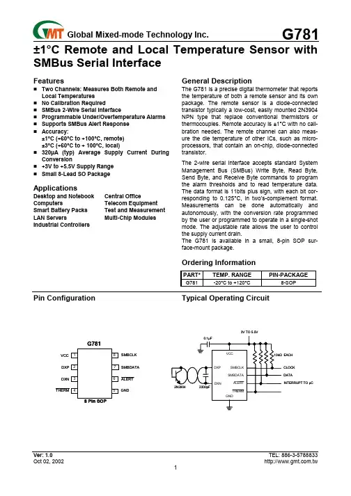
±1°C Remote and Local Temperature Sensor with SMBus Serial InterfaceFeaturesTwo Channels: Measures Both Remote andLocal Temperatures No Calibration RequiredSMBus 2-Wire Serial InterfaceProgrammable Under/Overtemperature Alarms Supports SMBus Alert Response Accuracy:±1°C (+60°C to +100°C, remote) ±3°C (+60°C to + 100°C, local)320µA (typ) Average Supply Current During Conversion+3V to +5.5V Supply Range Small 8-Lead SO PackageApplications Desktop and Notebook Central Office Computers Telecom Equipment Smart Battery Packs Test and Measurement LAN Servers Multi-Chip Modules Industrial Controllers General DescriptionThe G781 is a precise digital thermometer that reports the temperature of both a remote sensor and its own package. The remote sensor is a diode-connected transistor typically a low-cost, easily mounted 2N3904 NPN type that replace conventional thermistors or thermocouples. Remote accuracy is ±1°C with no cali-bration needed. The remote channel can also meas-ure the die temperature of other ICs, such as micro-processors, that contain an on-chip, diode-connected transistor.The 2-wire serial interface accepts standard System Management Bus (SMBus) Write Byte, Read Byte, Send Byte, and Receive Byte commands to program the alarm thresholds and to read temperature data.The data format is 11bits plus sign, with each bit cor-responding to 0.125°C, in two’s-complement format. Measurements can be done automatically and autonomously, with the conversion rate programmed by the user or programmed to operate in a single-shot mode. The adjustable rate allows the user to control the supply current drain.The G781 is available in a small, 8-pin SOP sur-face-mount package.Ordering InformationPART* TEMP. RANGE PIN-PACKAGEG781-20°C to +120°C8-SOPPin ConfigurationTypical Operating Circuit3V TO 5.5VEACHCLOCK DATAINTERRUPT TO µCSMBDATA SMBCLK GNDG781ALERTAbsolute Maximum RatingsVCC to GND………….….……..………….-0.3V to +6V DXP to GND……….……………..…-0.3V to VCC + 0.3V DXN to GND……………..……………..-0.3V to +0.8V SMBCLK, SMBDATA,ALERT to GND..…-0.3V to +6V SMBDATA,ALERT Current………….-1mA to +50mA DXN Current……………………..………………….±1mA ESD Protection (SMBCLK, SMBDATA,ALERT , humanbody model).……………………………………….2000V ESD Protection (other pins, human body model)..2000V Continuous Power Dissipation (T A = +70°C) ..SOP (derate 8.30mW/°C above +70°C)…………......667mW Operating Temperature Range………-20°C to +120°C Junction Temperature………………….………..+150°C Storage temperature Range………….-65°C to +165°C Lead Temperature (soldering, 10sec)……..……...+300°CStresses beyond those listed under “Absolute Maximum Ratings” may cause permanent damage to the device. These are stress ratings only, and functional operation of the device at these or any other conditions beyond those indicated in the opera-tional sections of the specifications is not implied. Exposure to absolute maximum rating conditions for extended periods may affect device reliability.Electrical Characteristics(VCC = + 3.3V, T A = 0°C to +85°C, unless otherwise noted.)PARAMETER CONDITIONS MIN TYP MAX UNITST R = +60°C to +100°C, VCC = 3.0V to 3.6V-1+1Temperature Error, Remote Di-ode (Note 1)T R = 0°C to +125°C (Note 2)-3 +3 °CT A = +60°C to +100°C-3 +3Temperature Error, Local DiodeT A = 0°C to +85°C (Note 2)-5 +5°CSupply-Voltage Range3.0 5.5 V Undervoltage Lockout Threshold VCC input, disables A/D conversion, rising edge 2.8 V Undervoltage Lockout Hysteresis 50 mV Power-On Reset Threshold VCC, falling edge 1.7 V POR Threshold Hysteresis 50 mVSMBus static3Standby Supply Current Logic inputs forced to VCC or GND Hardware or softwarestandby, SMBCLK at 10kHz4 µA0.5 conv/sec 35Average Operating Supply CurrentAuto-convert mode. Logic inputs forced to VCC or GND 8.0 conv/sec 320 µAConversion Time From stop bit to conversion complete (both channels) 125 ms Conversion Rate Timing Conversion-Rate Control Byte=04h, 1Hz 1 sec High level176Remote-Diode Source CurrentDXP forced to 1.5VLow level11µAElectrical Characteristics (continued)(VCC = + 3.3V, T A = 0 to +85°C, unless otherwise noted.)Note 1: A remote diode is any diode-connected transistor from Table1. T R is the junction temperature of the remote of the remote diode. See Remote Diode Selection for remote diode forward voltage requirements.Note 2: Guaranteed by design but not 100% tested.Pin DescriptionDetailed DescriptionThe G781 is a temperature sensor designed to work in conjunction with an external microcontroller (µC) or other intelligence in thermostatic, process-control, or monitoring applications. The µC is typically a power- management or keyboard controller, generating SMBus serial commands by “bit-banging” general- purpose input-output (GPIO) pins or via a dedicated SMBus interface block.Essentially an serial analog-to digital converter (ADC) with a sophisticated front end, the G781 contains a switched current source, a multiplexer, an ADC, an SMBus interface, and associated control logic (Figure 1). Temperature data from the ADC is loaded into two data registers, where it is automatically compared with data previously stored in several over/under- tem-perature alarm registers.ADC and MultiplexerThe ADC is an averaging type that integrates over a 60ms period (each channel, typical), with excellent noise rejection.The multiplexer automatically steers bias currents through the remote and local diodes, measures their forward voltages, and computes their temperatures. Both channels are automatically converted once the conversion process has started, either in free-running or single-shot mode. If one of the two channels is not used, the device still performs both measurements, and the user can simply ignore the results of the un-used channel. If the remote diode channel is unused, tie DXP to DXN rather than leaving the pins open. The worst-case DXP-DXN differential input voltage range is 0.25V to 0.95V.Excess resistance in series with the remote diode causes about +0.6°C error per ohm. Likewise, 240µV of offset voltage forced on DXP-DXN causes about 1°C error.Figure 1. Functional DiagramSMBDATA SMBCLKA/D Conversion SequenceIf a Start command is written (or generated automati-cally in the free-running auto-convert mode), both channels are converted, and the results of both meas-urements are available after the end of conversion. A BUSY status bit in the status byte shows that the de-vice is actually performing a new conversion; however, even if the ADC is busy, the results of the previous conversion are always available.Remote Diode SelectionTemperature accuracy depends on having a good- quality, diode-connected small-signal transistor. The G781 can also directly measure the die temperature of CPUs and other integrated circuits having on-board temperature-sensing diodes.The transistor must be a small-signal type with a rela-tively high forward voltage; otherwise, the A/D input voltage range can be violated. The forward voltage must be greater than 0.25V at 10µA; check to ensure this is true at the highest expected temperature. The forward voltage must be less than 0.95V at 300µA; check to ensure this is true at the lowest expected temperature. Large power transistors don’t work at all. Also, ensure that the base resistance is less than 100Ω. Tight specifications for forward-current gain (+50 to +150, for example) indicate that the manufac-turer has good process controls and that the devices have consistent V be characteristics.Thermal Mass and Self-HeatingThermal mass can seriously degrade the G781’s ef-fective accuracy. The thermal time constant of the SOP- package is about 140 in still air. For the G781 junction temperature to settle to within +1°C after a sudden +100°C change requires about five time con-stants or 12 minutes. The use of smaller packages for remote sensors, such as SOT23s, improves the situa-tion. Take care to account for thermal gradients be-tween the heat source and the sensor, and ensure that stray air currents across the sensor package do not interfere with measurement accuracy. Self-heating does not significantly affect measurement accuracy. Remote-sensor self-heating due to the diode current source is negligible. For the local diode, the worst-case error occurs when auto-converting at the fastest rate and simultaneously sinking maximum current at the ALERT output. For example, at an 8Hz rate and with ALERT sinking 1mA, the typical power dissipation isVCC x 320µA plus 0.4V x 1mA. Package theta J-A is about 120°C /W, so with VCC = 3.3V and no copper PC board heat-sinking, the resulting temperature rise is:dT =1.45mW x 120°C /W =0.17°CEven with these contrived circumstances, it is difficultto introduce significant self-heating errors.Table 1. Remote-Sensor Transistor Manufacturers MANUFACTURER MODELNUMBER Philips PMBS3904Motorola(USA) MMBT3904 National Semiconductor (USA) MMBT3904Note:Transistors must be diode-connected (baseshorted to collector).ADC Noise FilteringThe ADC is an integrating type with inherently good noise rejection. Micropower operation places con-straints on high-frequency noise rejection; therefore, careful PC board layout and proper external noise fil-tering are required for high-accuracy remote meas-urements in electrically noisy environments.High-frequency EMI is best filtered at DXP and DXNwith an external 2200pF capacitor. This value can be increased to about 3300pF(max), including cable ca-pacitance. Higher capacitance than 3300pF introduces errors due to the rise time of the switched current source.Nearly all noise sources tested cause the ADC meas-urements to be higher than the actual temperature, typically by +1°C to 10°C, depending on the frequencyand amplitude.PC Board LayoutPlace the G781 as close as practical to the remote diode. In a noisy environment, such as a computer motherboard, this distance can be 4 in. to 8 in. (typical)or more as long as the worst noise sources (such as CRTs, clock generators, memory buses, and ISA/PCI buses) are avoided.Do not route the DXP-DXN lines next to the deflection coils of a CRT. Also, do not route the traces across a fast memory bus, which can easily introduce +30°C error, even with good filtering, Otherwise, most noise sources are fairly benign.Route the DXP and DXN traces in parallel and in close proximity to each other, away from any high-voltage traces such as +12V DC. Leakage currents from PC board contamination must be dealt with carefully, since a 10MΩ leakage path from DXP to ground causes about +1°C error.Connect guard traces to GND on either side of the DXP-DXN traces (Figure 2). With guard traces in place, routing near high-voltage traces is no longer an issue.Route through as few vias and crossunders as possible to minimize copper/solder thermocouple ef-fects.When introducing a thermocouple, make sure that both the DXP and the DXN paths have matching thermocouples. In general, PC board-induced ther-mocouples are not a serious problem, A copper-solder thermocouple exhibits 3µV/°C, and it takes about 240µV of voltage error at DXP-DXN to cause a +1°C measurement error. So, most parasitic thermocouple errors are swamped out.Use wide traces. Narrow ones are more inductive and tend to pick up radiated noise. The 10 mil widths and spacing recommended on Figure 2 aren’t absolutely necessary (as they offer only a minor improvement in leakage and noise), but try to use them where practi-cal.Keep in mind that copper can’t be used as an EMI shield, and only ferrous materials such as steel work will. Placing a copper ground plane between the DXP-DXN traces and traces carrying high-frequency noise signals does not help reduce EMI.PC Board Layout ChecklistPlace the G781 close to a remote diode.Keep traces away from high voltages (+12V bus).Keep traces away from fast data buses and CRTs. Use recommended trace widths and spacing.Place a ground plane under the tracesUse guard traces flanking DXP and DXN and con necting to GND.Place the noise filter and the 0.1µF VCC bypass capacitors close to the G781.Figure 2. Recommended DXP/DXN PC Traces Twisted Pair and Shielded CablesFor remote-sensor distances longer than 8 in., or in particularly noisy environments, a twisted pair is rec-ommended. Its practical length is 6 feet to 12feet (typi cal) before noise becomes a problem, as tested in a noisy electronics laboratory. For longer distances, the best solution is a shielded twisted pair like that used for audio microphones. Connect the twisted pair to DXP and DXN and the shield to GND, and leave the shield’s remote end unterminated.Excess capacitance at DX_limits practical remote sen-sor distances (see Typical Operating Characteristics), For very long cable runs, the cable’s parasitic capaci-tance often provides noise filtering, so the 2200pF ca-pacitor can often be removed or reduced in value. Ca-ble resistance also affects remote-sensor accuracy; 1Ωseries resistance introduces about + 0.6°C error.Low-Power Standby ModeStandby mode disables the ADC and reduces the supply-current drain to about 10µA. Enter standby mode by forcing high to the RUN/STOP bit in the con-figuration byte register. Software standby mode be-haves such that all data is retained in memory, and the SMB interface is alive and listening for reads and writes.Software standby mode is not a shutdown mode. With activity on the SMBus, extra supply current is drawn (see Typical Operating Characteristics). In software standby mode, the G781 can be forced to perform A/D conversions via the one-shot command, despite the RUN/STOP bit being high.10 MILSMINIMUM10 MILS10 MILSIf software standby command is received while a con-version is in progress, the conversion cycle is trun-cated, and the data from that conversion is not latched into either temperature reading register. The previous data is not changed and remains available.Supply-current drain during the 125ms conversion period is always about 320µA. Slowing down the con-version rate reduces the average supply current (see Typical Operating Characteristics). In between con-versions, the instantaneous supply current is about 25µA due to the current consumed by the conversion rate timer. In standby mode, supply current drops to about 3µA. At very low supply voltages (under the power-on-reset threshold), the supply current is higher due to the address pin bias currents. It can be as high as 100µA, depending on ADD0 and ADD1 settings. SMBus Digital InterfaceFrom a software perspective, the G781 appears as a set of byte-wide registers that contain temperature data, alarm threshold values, or control bits, A stan-dard SMBus 2-wire serial interface is used to read temperature data and write control bits and alarm threshold data.Each A/D channel within the device responds to the same SMBus slave address for normal reads and writes.The G781 employs four standard SMBus protocols: Write Byte, Read Byte, Send Byte, and Receive Byte (Figure 3). The shorter Receive Byte protocol allows quicker transfers, provided that the correct data regis-ter was previously selected by a Read Byte instruction. Use caution with the shorter protocols in multi-master systems, since a second master could overwrite the command byte without informing the first master.The temperature data format is 11bits plus sign in twos-complement form for remote channel, with each data bit representing 0.125°C (Table 2,Table 3), transmitted MSB first. Table 2. Temperature Data Format(Two’s-Complement)DIGITAL OUTPUTDATA BITSTEMP.(°C)SIGN MSB LSB EXT+127.875 0 111 1111 111+126.375 0 111 1110 011+25.5 0 001 1001 100+1.75 0 000 0001 110+0.5 0 000 0000 100+0.125 0 000 0000 001-0.125 1 111 1111 111-1.125 1 111 1110 111-25.5 1 110 0110 100-55.25 1 100 1000 110-65.000 1 011 1111 000Table 3. Extended Temperature Data FormatEXTENDEDRESOLUTIONDATA BITS0.000°C 000000000.125°C 001000000.250°C 010000000.375°C 011000000.500°C 100000000.625°C 101000000.750°C 110000000.875°C 11100000Slave AddressThe G781 appears to the SMBus as one device hav-ing a common address for both ADC channels. The G781 device address is set to 1001100.The G781 also responds to the SMBus Alert Re-sponse slave address (see the Alert Response Ad-dress section).One-Shot RegisterThe One-shot register is to initiate a single conversion and comparison cycle when the device is in standby mode and auto conversion mode. The write operation to this register causes one-shot conversion and the data written to it is irrelevant and is not stored.Serial Bus Interface ReinitializationWhen SMBCLK are held low for more than 30ms (typical) during an SMBus communication the G781 will reinitiateits bus interface and be ready for a new transmission. Alarm Threshold RegistersFour registers store alarm threshold data, with high-temperature (T HIGH) and low-temperature (T LOW) registers for each A/D channel. If either measured temperature equals or exceeds the corresponding alarm threshold value, an ALERT interrupt is as-serted.The power-on-reset (POR) state of both T HIGH registers is full scale (01010101, or +85°C). The POR state of both T LOW registers is 0°C.Diode Fault AlarmThere is a fault detector at DXP that detects whether the remote diode has an open-circuit condition. At the beginning of each conversion, the diode fault is checked, and the status byte is updated. This fault de-tector is a simple voltage detector. If DXP rises above VCC – 1V (typical) due to the diode current source, a fault is detected and the device alarms through pulling ALERT low while the remote temperature reading doesn’t update in this condition. Note that the diode fault isn’t checked until a conversion is initiated, so im-mediately after power-on reset the status byte indicates no fault is present, even if the diode path is broken.If the remote channel is shorted (DXP to DXN or DXP to GND), the ADC reads 1000 0000(-128°C) so as not to trip either the T HIGH or T LOW alarms at their POR settings. ALERT InterruptsThe ALERT interrupt output signal is latched and canonly be cleared by reading the Alert Response ad-dress. Interrupts are generated in response to T HIGHand T LOW comparisons and when the remote diode is disconnected (for fault detection). The interrupt doesnot halt automatic conversions; new temperature datacontinues to be available over the SMBus interfaceafter ALERT is asserted. The interrupt output pin isopen-drain so that devices can share a common in-terrupt line. The interrupt rate can never exceed theconversion rate.The interface responds to the SMBus Alert Responseaddress, an interrupt pointer return-address feature(see Alert Response Address section). Prior to takingcorrective action, always check to ensure that an in-terrupt is valid by reading the current temperature.Alert Response AddressThe SMBus Alert Response interrupt pointer providesquick fault identification for simple slave devices thatlack the complex, expensive logic needed to be a busmaster. Upon receiving an ALERT interrupt signal,the host master can broadcast a Receive Byte trans-mission to the Alert Response slave address (0001100). Then any slave device that generated an inter-rupt attempts to identify itself by putting its own ad-dress on the bus (Table 4).The Alert Response can activate several differentslave devices simultaneously, similar to the SMBusGeneral Call. If more than one slave attempts to re-spond, bus arbitration rules apply, and the device withthe lower address code wins. The losing device doesnot generate an acknowledge and continues to holdthe ALERT line low until serviced (implies that thehost interrupt input is level-sensitive). Successfulreading of the alert response address clears the inter-rupt latch.Table 4. Read Format for Alert Response Address(0001 100)BIT NAME7(MSB) ADD76 ADD65 ADD54 ADD43 ADD32 ADD21 ADD10(LSB) 1Command Byte FunctionsThe 8-bit command byte register (Table 5) is the mas-ter index that points to the various other registers within the G781. The register’s POR state is 0000 0000, so that a Receive Byte transmission (a protocol that lacks the command byte) that occurs immediately after POR returns the current local temperature data.The one-shot command immediately forces a new conversion cycle to begin. In software standby mode (RUN/STOP bit = high), a new conversion is begun, after which the device returns to standby mode. If a conversion is in progress when a one-shot command is received in auto-convert mode (RUN/STOP bit = low) between conversions, a new conversion begins, the conversion rate timer is reset, and the next auto-matic conversion takes place after a full delay elapses.Configuration Byte FunctionsThe configuration byte register (Table 6) is used to mask interrupts and to put the device in software standby mode. The other bits are empty. Status Byte FunctionsThe status byte register (Table 7) indicates which (if any) temperature thresholds have been exceeded. This byte also indicates whether or not the ADC is converting and whether there is an open circuit in the remote diode DXP-DXN path. After POR, the normal state of all the flag bits is zero, assuming none of the alarm conditions are present. The status byte is cleared by any successful read of the status, unless the fault persists. Note that the ALERT interrupt latch is not automatically cleared when the status flag bit is cleared.When reading the status byte, you must check for in-ternal bus collisions caused by asynchronous ADC timing, or else disable the ADC prior to reading the status byte (via the RUN/STOP bit in the configura-tion byte). In one-shot mode, read the status byte only after the conversion is complete, which is approxi-mately 125ms max after the one-shot conversion is commanded.Table 5. Command-Byte Bit Assignments*If the device is in standby mode at POR, both temperature registers read 0°C.Table 6. Configuration-Byte Bit AssignmentsTable 7. Status-Byte Bit Assignments*These flags stay high until cleared by POR, or until the status byte register is read.Table 8. Conversion-Rate Control ByteDATA CONVERSION RATE (Hz)00h 0.062501h 0.12502h 0.2503h 0.504h 105h 206h 407h 808h 16 09h to FFh RFUTo check for internal bus collisions, read the status byte. If the least significant seven bits are ones, dis-card the data and read the status byte again. The status bits LHIGH, LLOW, RHIGH, and RLOW are refreshed on the SMBus clock edge immediately fol-lowing the stop condition, so there is no danger of los-ing temperature-related status data as a result of an internal bus collision. The OPEN status bit (diode con-tinuity fault) is only refreshed at the beginning of a conversion, so OPEN data is lost. The ALERT inter-rupt latch is independent of the status byte register, so no false alerts are generated by an internal bus colli-sion. When auto-converting, if the THIGH and TLOW limits are close together, it’s possible for both high-temp and low-temp status bits to be set, depending on the amount of time between status read operations (espe-cially when converting at the fastest rate). In these circumstances, it’s best not to rely on the status bits to indicate reversals in long-term temperature changes and instead use a current temperature reading to es-tablish the trend direction.For bit 1 and bit 0, a high indicates a temperature alarm happened for remote and local diode respec-tively. THERM pin also asserts. These two bits wouldn’t be cleared when reading status byte.Conversion Rate ByteThe conversion rate register (Table 8) programs the time interval between conversions in free-running auto-convert mode. This variable rate control reduces the supply current in portable-equipment applications. The conversion rate byte’s POR state is 08h (16Hz). The G781 looks only at the 4 LSB bits of this register, so the upper 4 bits are “don’t care” bits, which should be set to zero. The conversion rate tolerance is ±25% at any rate setting.Valid A/D conversion results for both channels are available one total conversion time (125ms,typical) after initiating a conversion, whether conversion is initiated via the RUN/STOP bit, one-shot command, or initial power-up.POR AND UVLOThe G781 has a volatile memory. To prevent ambiguous power-supply conditions from corrupting the data in memory and causing erratic behavior, a POR voltage detector monitors VCC and clears the memory if VCC falls below 1.7V (typical, see Electrical Characteristics table). When power is first applied and VCC rises above 1.7V (typical), the logic blocks begin operating, although reads and writes at V CC levels below 3V are not recom-mended. A second VCC comparator, the ADC UVLO comparator, prevents the ADC from converting until there is sufficient headroom (VCC= 2.8V typical).ALERT Fault QueueTo suppress unwanted ALERT triggering the G781 em-bedded a fault queue function. The ALERT won’t as-sert until consecutive out of limit measurements have reached the queue number. The mapping of fault queue register (ALERTFQ, 22h) value to fault queue number is shown in the Table 9.Table 9. Alert Fault QueueALERTFQVALUEFAULT QUEUE NUMBER XXXX000X 1XXXX001X 2XXXX010X 3XXXX011X 3XXXX100X 4XXXX101X 4XXXX110X 4XXXX111X 4 Operation of The THERM FunctionA local and remote THERM limit can be programmed into the G781 to set the temperature limit above which the THERM pin asserts low and the bit 1, of status byte will be set to 1 corresponding to remote and local over temperature. These two bits won’t be cleared to 0 by reading status byte it the over temperature condi-tion remain. A hysteresis value is provided by writing the register 21h to set the temperature threshold to release the THERM pin alarm state, The releasing temperature is the value of register 19h, 20h minus the value in register 21h. The format of register 21h is 2’s complement. The THERM signal is open drain and requires a pull-up resistor to power supply.Figure 4. SMBus Write Timing DiagramA = start condition H = LSB of data clocked into slaveB = MSB of address clocked into slave I = slave pulls SMBDATA line lowC = LSB of address clocked into slave J = acknowledge clocked into masterD = R/W bit clocked into slave K = acknowledge clocked pulseE = slave pulls SMBDATA line low L = stop condition data executed by slaveF = acknowledge bit clocked into master M = new start conditionG = MSB of data clocked into slaveFigure 5. SMBus Read Timing DiagramA = start condition G = MSB of data clocked into masterB = MSB of address clocked into slave H = LSB of data clocked into masterC = LSB of address clocked into slave I = acknowledge clocked pulseD = R/W bit clocked into slave J = stop conditionE = slave pulls SMBDATA line low K= new start conditionF =acknowledge bit clocked into master。
Z515中文资料(Intel)中文数据手册「EasyDatasheet - 矽搜」

3.3 去耦指南................................................ ............................ 28
3.3.1 3.3.2
V CC 去耦................................................. ........................ 28 FSB AGTL +解耦............................................... ............... 28
Contact your local Intel sales office or your distributor to obtain the latest specifications and before placing your product order. Copie s of docum ents which have an orde r num be r and are re fere nce d in this docum ent, or othe r Inte l lite rature , m ay be obtaine d
Hyper-Threading Technology requires a com puter system with a processor supporting Hyper-Threading Technology and HT Technology enabled chipset, BIO S and operating system . Perform ance will vary depending on the specific hardware and software
MHW1815中文资料
–T–
SEATING PLANE
P 7 PL
CASE 301AK–01 ISSUE B
STYLE 1: PIN 1. 2. 3. 4. 5. 6. 7.
RF INPUT DC TERMINAL, Vs1 DC TERMINAL, Vs2 DC TERMINAL, Vb DC TERMINAL, Vs3 DC TERMINAL, Vs4 RF OUTPUT
PACKAGE DIMENSIONS
–A– G 1.02 (0.040)
M
T AND TOLERANCING PER ASME Y14.5M, 1994. 2. CONTROLLING DIMENSION: INCH. 3. DIMENSION F TO CENTER OF LEADS. 4. REF INDICATES NON–CONTROLLED DIMENSION FOR REFERENCE USE ONLY.
MHW1815 1
元器件交易网
RF IN
VS1 26 V
VS2 26 V
VBIAS VS3 5 V 26 V
VS4 26 V
RF OUT
Figure 1. Internal Diagram
MHW1815 2
MOTOROLA RF DEVICE DATA
元器件交易网
元器件交易网
MOTOROLA
The RF Line
SEMICONDUCTOR TECHNICAL DATA
Order this document by MHW1815/D
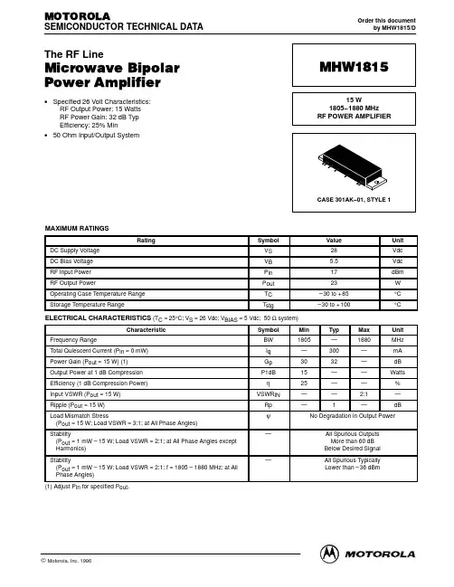
Microwave Bipolar Power Amplifier
• Specified 26 Volt Characteristics: RF Output Power: 15 Watts RF Power Gain: 32 dB Typ Efficiency: 25% Min • 50 Ohm Input/Output System
AV92中文资料
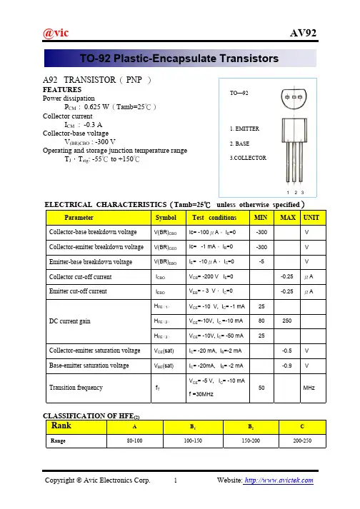
AV92
1. EMITTER 2. BASE 3.COLLECTOR
1
2 3
ELECTRICAL CHARACTERISTICS(Tamb=25℃ unless otherwise specified)
Parameter Collector-base breakdown voltage Collector-emitter breakdown voltage Emitter-base breakdown voltage Collector cut-off current Emitter cut-off current Symbol
Copyright © Avic Electronics Corp.
2
Website:
Base-Emitter ON Voltage vs Collector Current
-40 °C 0.6 0.4 0.2 1 10 IC - Collector Current (mA) 100 25 °C 125 °C VCE =5V
Collector-Cutoff Current vs Ambient Temperature ICBO- Collector Current (nA) 100 10 1 0.1 VCB =150V Capacitance (pF) 10
100
Base-Emitter Saturation Voltage vs Collector Current VBESAT - Base-Emitter Voltage (V) VBE(ON) - Base-Emitter On Voltage (V) 1.0 0.9 0.8 0.7 0.6 0.5 0.4 0.3 1 10 IC - Collector Current (mA) -40 °C 25 °C 125 °C =1 0 100 1 0.MAX
BSO615N中文资料
Parameter
Symbol
Continuous drain current, one channel active Pulsed drain current, one channel active
ID IDpulse
TA = 25 ˚C
Avalanche energy, single pulse
0.36
Ω
RDS(on)
0.28
0.24
0.20 98%
0.16 typ
0.12
0.08
0.04
0.00
-60
-20
20
60 100 ˚C
180
Tj
C
pF
Ciss
10 2
Coss Crss
10 1 0
5 10 15 20 25 30 V 40
VDS
Data Sheet
6
05.99
BSO 615N
ID
10 1
V
10 2
VDS
10
-1
10
-5
10 -4
10 -3
10 -2
10 -1
10 0
10 1
10 2
s 10 4
tp
Data Sheet
5
05.99
BSO 615N
Typ. output characteristics
ID = f (VDS)
parameter: tp = 80 µs
BSO 615N
EAS
ID = 2.6 A, VDD = 25 V, RGS = 25 Ω
Avalanche current,periodic limited by Tjmax Avalanche energy, periodic limited by Tjmax Reverse diode dv/dt
RLA910中文资料
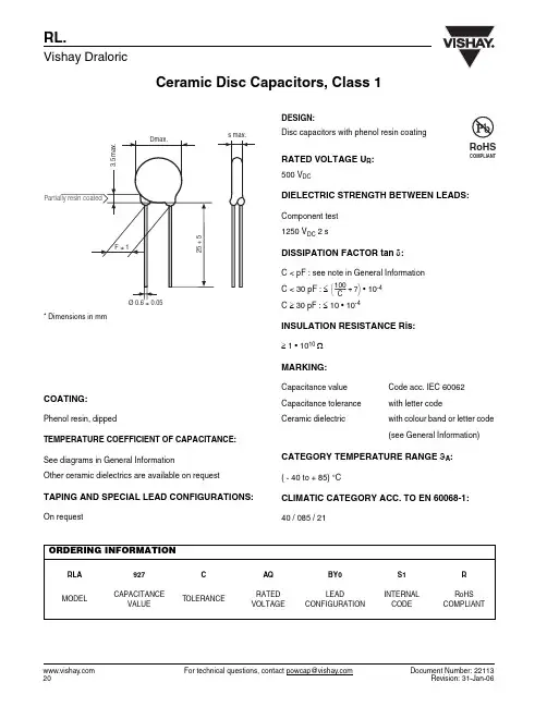
RL.Vishay DraloricCeramic Disc Capacitors, Class 1* Dimensions in mmCOATING:Phenol resin, dippedTEMPERATURE COEFFICIENT OF CAPACITANCE:See diagrams in General InformationOther ceramic dielectrics are available on requestTAPING AND SPECIAL LEAD CONFIGURATIONS:On requestDESIGN:Disc capacitors with phenol resin coatingRATED VOLTAGE U R :500 V DCDIELECTRIC STRENGTH BETWEEN LEADS:Component test1250 V DC 2 sDISSIPATION FACTOR tan δ:C < pF : see note in General InformationC < 30 pF : ≤ • 10-4C ≥ 30 pF : ≤ 10 • 10-4INSULATION RESISTANCE Ris:≥ 1 • 1010 ΩMARKING:Capacitance valueCode acc. IEC 60062Capacitance tolerance with letter codeCeramic dielectricwith colour band or letter code (see General Information)CATEGORY TEMPERATURE RANGE ϑA :( - 40 to + 85) °CCLIMATIC CATEGORY ACC. TO EN 60068-1:40 / 085 / 21100C---------7+⎝⎠⎛⎞ORDERING INFORMATIONRLA 927CAQ BY0S1R MODELCAPACITANCEVALUETOLERANCERATED VOLTAGELEADCONFIGURATIONINTERNAL CODERoHS COMPLIANTDocument Number: RL.Ceramic Disc Capacitors, Class 1Vishay Draloric* Standard lead configuration, other lead spacing and diameter available on request.ORDERING INFORMATION, CERAMIC DISC CAPACITORS, 500 V (DC)C (pF)TOL.(%)D x s (mm) F ± 1 *(mm) d ± 0.05 *(mm)CERAMIC CODEORDERING CODE CLASS 1 P 1001.0C < 10 pF± 0.25 pF ± 0.5 pF C ≥ 10 pF ± 5 %± 10 %7.5 x 5.0 5.00.6Red color dotor Letter ARLA910 AQ S1R 1.17.5 x 5.0RLA911 AQ S1R 1.27.5 x 5.0RLA912 AQ S1R 1.37.5 x 5.0RLA913 AQ S1R 1.57.5 x 5.0RLA915 AQ S1R 1.67.5 x 5.0RLA916 AQ S1R 1.87.5 x 5.0RLA918 AQ S1R 2.07.5 x 5.0RLA920 AQ S1R 2.27.5 x 5.0RLA922 AQ S1R 2.47.5 x 5.0RLA924 AQ S1R 2.77.5 x 5.0RLA927 AQ S1R 3.07.5 x 5.0RLA930 AQ S1R 3.37.5 x 5.0RLA933 AQ S1R 3.67.5 x 5.0RLA936 AQ S1R 3.97.5 x 5.0RLA939 AQ S1R 4.310.0 x 5.0RLA943 AQ S1R 4.710.0 x 5.0RLA947 AQ S1R 5.110.0 x 5.0RLA951 AQ S1R 5.610.0 x 5.0RLA956 AQ S1R 6.210.0 x 5.0RLA962 AQ S1R 6.810.0 x 5.0RLA968 AQ S1R 7.510.0 x 5.0RLA975 AQ S1R 8.210.0 x 5.0RLA982 AQ S1R 9.114.0 x 5.07.5RLA991 AQ S1R 1014.0 x 5.0RLA100 AQ S1R CLASS 1 NP 01.5C < 10 pF± 0.25 pF ± 0.5 pF C ≥ 10 pF ± 5 %± 10 %7.5 x 5.0 5.00.6Black color dotor Letter CRLC915 AQ S1R 1.67.5 x 5.0RLC916 AQ S1R 1.87.5 x 5.0RLC918 AQ S1R 2.07.5 x 5.0RLC920 AQ S1R 2.27.5 x 5.0RLC922 AQ S1R 2.47.5 x 5.0RLC924 AQ S1R 2.77.5 x 5.0RLC927 AQ S1R 3.07.5 x 5.0RLC930 AQ S1R 3.37.5 x 5.0RLC933 AQ S1R 3.67.5 x 5.0RLC936 AQ S1R 3.97.5 x 5.0RLC939 AQ S1R 4.37.5 x 5.0RLC943 AQ S1R 4.77.5 x 5.0RLC947 AQ S1R 5.17.5 x 5.0RLC951 AQ S1R 5.67.5 x 5.0RLC956 AQ S1R 6.27.5 x 5.0RLC962 AQ S1R 6.87.5 x 5.0RLC968 AQ S1R 7.57.5 x 5.0RLC975 AQ S1R 8.27.5 x 5.0RLC982 AQ S1R 9.17.5 x 5.0RLC991 AQ S1R 1010.0 x 5.0RLC100 AQ S1R 1110.0 x 5.0RLC110 AQ S1R 1210.0 x 5.0RLC120 AQ S1R 1310.0 x 5.0RLC130 AQ S1R 1510.0 x 5.0RLC150 AQ S1R 1614.0 x 5.07.5RLC160 AQ S1R 1814.0 x 5.0RLC180 AQ S1R 2014.0 x 5.0RLC200 AQ S1R 2214.0 x 5.0RLC220 AQ S1RORDERING CODE7th digitCapacitance tolerance± 0.25 pF = C ± 0.5 pF = D ± 5 % = J ± 10 % = K10th / 11th / 12th digit Lead configuration (See General Information)R 14th digit RoHS Compliant Component For technical questions, contact powcap@Document Number: 22113RL.Vishay DraloricCeramic Disc Capacitors, Class 1* Standard lead configuration, other lead spacing and diameter available on request.ORDERING INFORMATION, CERAMIC DISC CAPACITORS, 500 V (DC)C (pF)TOL.(%)D x s (mm) F ± 1 *(mm) d ± 0.05 *(mm)CERAMIC CODEORDERING CODE CLASS 1 N 1502.2C < 10 pF± 0.25 pF ± 0.5 pF C ≥ 10 pF ± 5 %± 10 %7.5 x 5.0 5.00.6Orange colordotor Letter PRLP922 AQ S1R 2.47.5 x 5.0RLP924 AQ S1R 2.77.5 x 5.0RLP927 AQ S1R 3.07.5 x 5.0RLP930 AQ S1R 3.37.5 x 5.0RLP933 AQ S1R 3.67.5 x 5.0RLP936 AQ S1R 3.97.5 x 5.0RLP939 AQ S1R 4.37.5 x 5.0RLP943 AQ S1R 4.77.5 x 5.0RLP947 AQ S1R 5.17.5 x 5.0RLP951 AQ S1R 5.67.5 x 5.0RLP956 AQ S1R 6.27.5 x 5.0RLP962 AQ S1R 6.87.5 x 5.0RLP968 AQ S1R 7.57.5 x 5.0RLP975 AQ S1R 8.27.5 x 5.0RLP982 AQ S1R 9.17.5 x 5.0RLP991 AQ S1R 107.5 x 5.0RLP100 AQ S1R 1110.0 x 5.0RLP110 AQ S1R 1210.0 x 5.0RLP120 AQ S1R 1310.0 x 5.0RLP130 AQ S1R 1510.0 x 5.0RLP150 AQ S1R 1610.0 x 5.0RLP160 AQ S1R 1810.0 x 5.0RLP180 AQ S1R 2010.0 x 5.0RLP200 AQ S1R 2210.0 x 5.0RLP220 AQ S1R 2410.0 x 5.0RLP240 AQ S1R 2714.0 x 5.07.5RLP270 AQ S1R 3014.0 x 5.0RLP300 AQ S1R 3314.0 x 5.0RLP330 AQ S1R CLASS 1 N 7503.3C < 10 pF± 0.25 pF ± 0.5 pF C ≥ 10 pF ± 5 %± 10 %7.5 x 5.0 5.00.6Violet color dotor Letter URLU933 AQ S1R 3.67.5 x 5.0RLU936 AQ S1R 3.97.5 x 5.0RLU939 AQ S1R 4.37.5 x 5.0RLU943 AQ S1R 4.77.5 x 5.0RLU947 AQ S1R 5.17.5 x 5.0RLU951 AQ S1R 5.67.5 x 5.0RLU956 AQ S1R 6.27.5 x 5.0RLU962 AQ S1R 6.87.5 x 5.0RLU968 AQ S1R 7.57.5 x 5.0RLU975 AQ S1R 8.27.5 x 5.0RLU982 AQ S1R 9.17.5 x 5.0RLU991 AQ S1R 107.5 x 5.0RLU100 AQ S1R 117.5 x 5.0RLU110 AQ S1R 127.5 x 5.0RLU120 AQ S1R 137.5 x 5.0RLU130 AQ S1R 157.5 x 5.0RLU150 AQ S1R 167.5 x 5.0RLU160 AQ S1R 187.5 x 5.0RLU180 AQ S1R 207.5 x 5.0RLU200 AQ S1R 227.5 x 5.0RLU220 AQ S1R 247.5 x 5.0RLU240 AQ S1R 277.5 x 5.0RLU270 AQ S1R 3010.0 x 5.0RLU300 AQ S1R 3310.0 x 5.0RLU330 AQ S1R 3610.0 x 5.0RLU360 AQ S1R 3910.0 x 5.0RLU390 AQ S1R 4310.0 x 5.0RLU430 AQ S1R 4710.0 x 5.0RLU470 AQ S1R 5110.0 x 5.0RLU510 AQ S1R 5610.0 x 5.0RLU560 AQ S1R 6214.0 x 5.07.5RLU620 AQ S1R 6814.0 x 5.0RLU680 AQ S1RDocument Number: RL.Ceramic Disc Capacitors, Class 1Vishay Draloric* Standard lead configuration, other lead spacing and diameter available on request.ORDERING INFORMATION, CERAMIC DISC CAPACITORS, 500 V (DC)C (pF)TOL.(%)D x s (mm) F ± 1 *(mm) d ± 0.05 *(mm)CERAMIC CODEORDERING CODE CLASS 1 N 15003.3C < 10 pF± 0.25 pF ± 0.5 pF C ≥ 10 pF ± 5 %± 10 %7.0 x 5.0 5.00.6Orange / Orange colordotsor Letter VRLV933 AQ S1R 3.67.0 x 5.0RLV936 AQ S1R 3.97.0 x 5.0RLV939 AQ S1R 4.37.0 x 5.0RLV943 AQ S1R 4.77.0 x 5.0RLV947 AQ S1R 5.17.0 x 5.0RLV951 AQ S1R 5.67.0 x 5.0RLV956 AQ S1R 6.27.0 x 5.0RLV962 AQ S1R 6.87.0 x 5.0RLV968 AQ S1R 7.57.0 x 5.0RLV975 AQ S1R 8.27.0 x 5.0RLV982 AQ S1R 9.17.0 x 5.0RLV991 AQ S1R 107.0 x 5.0RLV100 AQ S1R 117.0 x 5.0RLV110 AQ S1R 127.0 x 5.0RLV120 AQ S1R 137.0 x 5.0RLV130 AQ S1R 157.0 x 5.0RLV150 AQ S1R 167.0 x 5.0RLV160 AQ S1R 187.0 x 5.0RLV180 AQ S1R 207.0 x 5.0RLV200 AQ S1R 227.0 x 5.0RLV220 AQ S1R 247.0 x 5.0RLV240 AQ S1R 277.0 x 5.0RLV270 AQ S1R 307.0 x 5.0RLV300 AQ S1R 337.0 x 5.0RLV330 AQ S1R 367.0 x 5.0RLV360 AQ S1R 397.0 x 5.0RLV390 AQ S1R 437.0 x 5.0RLV430 AQ S1R 477.0 x 5.0RLV470 AQ S1R 5110.0 x 5.0RLV510 AQ S1R 5610.0 x 5.0RLV560 AQ S1R 6210.0 x 5.0RLV620 AQ S1R 6810.0 x 5.0RLV680 AQ S1R 7510.0 x 5.0RLV750 AQ S1R 8214.0 x 5.07.5RLV820 AQ S1R 9114.0 x 5.0RLV910 AQ S1R 10014.0 x 5.0RLV101 AQ S1RORDERING CODE7th digitCapacitance tolerance± 0.25 pF = C ± 0.5 pF = D ± 5 % = J ± 10 % = K10th / 11th / 12th digit Lead configuration (See General Information)R 14th digit RoHS Compliant Component For technical questions, contact powcap@Document Number: 22113RL.Vishay DraloricCeramic Disc Capacitors, Class 1* Standard lead configuration, other lead spacing and diameter available on request.ORDERING INFORMATION, CERAMIC DISC CAPACITORS, 500 V (DC)C (pF)TOL.(%)D x s (mm) F ± 1 *(mm) d ± 0.05 *(mm)CERAMIC CODEORDERING CODE CLASS 1 N 22005.6C < 10 pF± 0.25 pF ± 0.5 pF C ≥ 10 pF ± 5 %± 10 %7.0 x 5.0 5.00.6Y ellow / Orange color dotsor Letter KRLK956 AQ S1R 6.27.0 x 5.0RLK962 AQ S1R 6.87.0 x 5.0RLK968 AQ S1R 7.57.0 x 5.0RLK975 AQ S1R 8.27.0 x 5.0RLK982 AQ S1R 9.17.0 x 5.0RLK991 AQ S1R 107.0 x 5.0RLK100 AQ S1R 117.0 x 5.0RLK110 AQ S1R 127.0 x 5.0RLK120 AQ S1R 137.0 x 5.0RLK130 AQ S1R 157.0 x 5.0RLK150 AQ S1R 167.0 x 5.0RLK160 AQ S1R 187.0 x 5.0RLK180 AQ S1R 207.0 x 5.0RLK200 AQ S1R 227.0 x 5.0RLK220 AQ S1R 247.0 x 5.0RLK240 AQ S1R 277.0 x 5.0RLK270 AQ S1R 307.0 x 5.0RLK300 AQ S1R 337.0 x 5.0RLK330 AQ S1R 367.0 x 5.0RLK360 AQ S1R 397.0 x 5.0RLK390 AQ S1R 437.0 x 5.0RLK430 AQ S1R 477.0 x 5.0RLK470 AQ S1R 517.0 x 5.0RLK510 AQ S1R 567.0 x 5.0RLK560 AQ S1R 6210.0 x 5.0RLK620 AQ S1R 6810.0 x 5.0RLK680 AQ S1R 7510.0 x 5.0RLK750 AQ S1R 8210.0 x 5.0RLK820 AQ S1R 9110.0 x 5.0RLK910 AQ S1R 10010.0 x 5.0RLK101 AQ S1R 11010.0 x 5.0RLK111 AQ S1R 12010.0 x 5.0RLK121 AQ S1R 13014.0 x 5.07.5RLK131 AQ S1R 15014.0 x 5.0RLK151 AQ S1R 16014.0 x 5.0RLK161 AQ S1R 18014.0 x 5.0RLK181 AQ S1R CLASS 1 N 560036± 5 %± 10 %7.0 x 5.0 5.00.6Blue / Orange color dotsor Letter MRLM360 AQ S1R 397.0 x 5.0RLM390 AQ S1R 477.0 x 5.0RLM470 AQ S1R 567.0 x 5.0RLM560 AQ S1R 687.0 x 5.0RLM680 AQ S1R 827.0 x 5.0RLM820 AQ S1R 1007.0 x 5.0RLM101 AQ S1R 1207.0 x 5.0RLM121 AQ S1R 15010.0 x 5.07.5RLM151 AQ S1R 18010.0 x 5.0RLM181 AQ S1R 22010.0 x 5.0RLM221 AQ S1R 27010.0 x 5.0RLM271 AQ S1R 33010.0 x 5.0RLM331 AQ S1RORDERING CODE7th digitCapacitance tolerance± 0.25 pF = C ± 0.5 pF = D ± 5 % = J ± 10 % = K10th / 11th / 12th digit Lead configuration (See General Information)R 14th digit RoHS Compliant ComponentDisclaimer Legal Disclaimer NoticeVishayAll product specifications and data are subject to change without notice.Vishay Intertechnology, Inc., its affiliates, agents, and employees, and all persons acting on its or their behalf (collectively, “Vishay”), disclaim any and all liability for any errors, inaccuracies or incompleteness contained herein or in any other disclosure relating to any product.Vishay disclaims any and all liability arising out of the use or application of any product described herein or of any information provided herein to the maximum extent permitted by law. The product specifications do not expand or otherwise modify Vishay’s terms and conditions of purchase, including but not limited to the warranty expressed therein, which apply to these products.No license, express or implied, by estoppel or otherwise, to any intellectual property rights is granted by this document or by any conduct of Vishay.The products shown herein are not designed for use in medical, life-saving, or life-sustaining applications unless otherwise expressly indicated. Customers using or selling Vishay products not expressly indicated for use in such applications do so entirely at their own risk and agree to fully indemnify Vishay for any damages arising or resulting from such use or sale. Please contact authorized Vishay personnel to obtain written terms and conditions regarding products designed for such applications.Product names and markings noted herein may be trademarks of their respective owners.元器件交易网。
思科 Cisco Catalyst 9105 系列无线接入点 产品手册
Cisco Catalyst 9105 系列无线接入点产品手册思科公开信息Cisco® Catalyst® 9105 系列无线接入点是下一代企业级无线接入点,具有灵活、安全可靠、智能省心的特点。
随着高密度网络和物联网的出现,我们比以往任何时候都更依赖于无线网络。
每年都有越来越多的设备连接到网络,从高性能客户端设备到低带宽物联网设备举不胜举,使现有网络的网速日益受到挑战。
Cisco Catalyst 9105 无线接入点可以随时随地为所有用户提供无缝体验,在各种网络部署中发挥卓越的可扩展性和出色的性能。
Catalyst 9105 无线接入点在支持 Wi-Fi 6 (802.11ax) 标准的基础上更进一步,能够实现安全性、恢复能力和运营灵活性的绝佳融合,并提供更强大的网络智能功能。
Catalyst 9105 无线接入点不仅可拓展思科基于意图的网络,而且可进行扩展以满足不断增长的物联网需求,并全面支持最新的创新成果和最新技术,因此适合用于各种规模的网络。
Catalyst 9105 无线接入点的性能、安全性和分析功能均处于领先水平。
根据安装方式,Catalyst 9105 分为两种型号:适用于天花板安装的 Catalyst 9105i 和适用于壁式安装的 Catalyst 9105w。
凭借独特的安装设计,Catalyst 9105w 非常适合酒店、学生宿舍和其他多住户单元。
Catalyst 9105 无线接入点还可以为远程员工和微型办公室提供安全保护。
所有 Cisco Aironet 或 Catalyst 无线接入点都可以作为OfficeExtend 无线接入点(OEAP) 使用。
通过 OEAP,员工无需设置VPN 或具备高深技术知识,即可在家中或临时的微型办公室中访问企业 SSID 和公司网络。
Cisco Catalyst 9105 系列无线接入点可结合思科全数字化网络架构 (Cisco DNA) 使用,是可满足您当前和未来需求的企业级产品。
MCP2551中文资料
CANH
高 未驱动 未驱动
高 未驱动 未驱动 未驱动 / 无负载
CANL
低 未驱动 未驱动
低 未驱动 未驱动 未驱动 / 无负载
注 1: 如果另一个总线节点在 CAN 总线上传送显性位,那么 RXD 是逻辑 ‘0’。 2: X = “不确定”。 3: 虽然输出不一定能满足 ISO-11898 规范,但是器件驱动器仍然能够工作。
1.7.2
接地端 (VSS)
接地引脚。
1.7.3
电源端 (VDD)
正电源引脚。
1.7.4 接收器数据输出 (RXD)
RXD 是一个 CMOS 兼容输出引脚,它根据 CANH 和 CANL 引脚上的差分信号决定驱动高电平还是低电平。 它通常与 CAN 控制器的接收器数据输入相连。当 CAN 总线为隐性时 RXD 处于高电平,当 CAN 总线为显性的 时候它为低电平。
1.1 发送器功能
CAN 总线有两个状态:显性状态和隐性状态。显性状态 发生在 CANH 和 CANL 之间的差分电压高于定义值(如 1.2V)的时候。隐性状态发生在该差分电压低于某个定 义值 (典型值为 0V)的时候。显性状态和隐性状态分 别对应于 TXD 输入引脚的低电平和高电平。但是,一 个由别的 CAN 节点触发的显性状态将会改写 CAN 总线 上的隐性状态。
2005 Microchip Technology Inc.
DS21667D_CN 第 3 页
MCP2551
表 1-1: 模式
待机 斜率控制 高速
操作模式 Rs 引脚电流
-IRS < 10 µA 10 µA < -IRS < 200 µA -IRS < 610 µA
RS 引脚上的电压
AD9851中文资料
特征180 MHz时钟速率参考时钟具有6倍倍乘器。
芯片具有高性能10位DAC和高速滞后比较器无杂散动态范围SFDR为43分贝@ 70 MHz的模拟输出。
32位频率控制字简化控制接口:并行或串行异步加载格式5位相位调制和补偿能力比较器纹波抖动<80 ps p-p @ 20 MHz+2.7 V至+5.25 V单电源工作低功耗: 555毫瓦@ 180兆赫省电功能, 4毫瓦@ 2.7 V超小28引线SSOP封装频带宽 正常输出工作频率范围为 0~72MHz ;应用频率/相敏正弦波合成为进行数字通信设定时钟恢复和锁定电路通信数字控制的ADC编码发生器敏捷L.O应用在正交振荡器连续波,调幅,调频, FSK信号,发射机的MSK模式。
概述该AD9851是一种高度集成的设备,采用先进的DDS技术,再加上内部高速度、高性能D / A转换器,和比较器,使一个数字可编程频率合成器和时钟发生器功能化。
当参照准确的时钟源,AD9851可以产生一个稳定的频率和相位且可数字化编程的模拟正弦波输出。
此正弦波可直接用作时钟源,在其内部转化为方波成为灵活的时钟发生器。
AD9851采用的最新的高速DDS内核可接受32位的频率控制字,180 MHz系统时钟,分辨率为0.04赫兹。
该AD9851包含一个特有的6 × REFCLK倍乘器电路,因此无需高速外部晶振。
6 × REFCLK倍乘器使其有最小的无杂散动态范围SFDR和相位噪声特性。
AD9851提供了5位可编程相位调制,使移相输出的增量为11.25°。
功能方框图该AD9851包含一个内部的高速比较器。
可以输出一个低抖动输出脉冲。
可进行频率调整,控制能将相位调谐字异步加载到AD9851并通过并行或串行方式载入。
并行负载格式由五个迭代的8位控制字(字节) 。
第一个8位字节控制输出相位, 6 × REFCLK倍乘器,电源关闭启用和装载模式;其余字节组成32位频率控制字。
EM91410D中文资料(ELAN Microelectronics)中文数据手册「EasyDatasheet - 矽搜」
ROW1~ROW4
COL1〜COL3和COL5
COL4/KT
XIN和XOUT XMUTE
V DD 和V HFI
SS
HFO
能时,该引脚切换到"高".否则,此引脚防护持"低"水平.
DTMF
DTMF(双音多频)和音乐信号输出引脚.通常情况下,该引脚防护持"低" 水平.在音频拨号模式,即对应于键盘0.9,*和#键此引脚输出DTMF信号.除这
引脚说明
符号 功能 行组键盘扫描引脚.在空闲状态(HKS为"高"和HFO为"低"),这些引脚呆" 高阻抗"级别,以防止功耗.否则,这些引脚切换到"高"级别以检测键盘输 入.这些引脚将输出600 Hz信号,同时键盘扫描. 栏目组键盘扫描引脚.在待机状态下,这些引脚留"高阻抗"水平.否则,这些 引脚切换到"低"电平检测键盘输入.这些引脚将输出600 Hz信号,同时键盘 扫描. 键盘第四列组销,它也提供基本色调输出 .通常情况下,该引脚防护持"低"电平检测键盘输入.经过有效 键盘输入,此引脚将输出键控确认音就是600赫兹信号 30毫秒时间.为防止信号干扰,同时DTMF问题,这将禁用键 音输出,除功能键. 振荡器输入和输出引脚.一个3.579545 MHz晶体或陶瓷谐振器必须 被交叉连接到XIN和XOUT其产生系统时钟. 音频/脉冲静音信号输出管脚,为NMOS漏极开路输出结构. 该引脚将在音频/脉冲拨号和防护持功能切换到"低"水平. 否则,此引脚防护持"高阻抗"水平. 正,负电源输入引脚.推荐工作电压从2.0Vdc至5.5VDC. 免提输入管脚,它接受下降沿信号以接通"上"或关闭"关"免提功能.该引 脚是滞后输入结构并内置上拉电阻(通常为200千欧).
- 1、下载文档前请自行甄别文档内容的完整性,平台不提供额外的编辑、内容补充、找答案等附加服务。
- 2、"仅部分预览"的文档,不可在线预览部分如存在完整性等问题,可反馈申请退款(可完整预览的文档不适用该条件!)。
- 3、如文档侵犯您的权益,请联系客服反馈,我们会尽快为您处理(人工客服工作时间:9:00-18:30)。
Error % +0.28
R2
770
766
-0.52
R3
852
R4
941
C1
1209
848 948 1216
-0.47 +0.74 +0.57
C2
1336
C3
1477
1332 1472
-0.30 -0.34
Publication Release Date: May 1997
-3-
Revision A2
Power input pins.
Key-tone signal output. The key tone is generated for all valid keys. Frequency is 600 Hz and duration is 35 mS.
In pulse mode, this pin remains in low state at all times.
Redialing
1. OFF HOOK (or ON HOOK & HFI ¡õ ), D1 , D2 , ..., Dn , Busy,
Yes
20
Publication Release Date: May 1997
-1-
Revision A2
PIN CONFIGURATIONS
W91510N SERIES
C1
1
C2
2
C3
3
C4
4
KT
5
VSS
6
XT
7
XT
8
T/P MUTE
9
18
R4
17
R3
16
R2
15
R1
14
VDD
13
MODE
12
DTMF
W91510N SERIES
Pin Description, continued
SYMBOL 18-PIN
HFI, HFO
-
20-PIN 10, 11
I/O
FUNCTION
I, O Handfree control pins. The handfree control state is
toggled on by a low pulse on the HFI input pin. The status of the handfree control state is described in the following table:
W91510N SERIES
TONE/PULSE DIALER WITH HANDFREE AND SAVE FUNCTIONS
GENERAL DESCRIPTION
The W91510N series are Si-gate CMOS ICs that provide the necessary signals for tone or pulse dialing. The W91510N series provide one-key redial, handfree dialing, key tone, save, and redial functions.
COUNTER
DATA LATCH & DECODER
MODE
KT T/P MUTE DP HFO
-4-
W91510N SERIES
FUNCTIONAL DESCRIPTION Keyboard Operation
C1 C2
1
2
4
5
7
8
∗/T
0
R/P2 R
C3 C4
3 SAVE R1
6
F1 R2
9
In tone mode, it will output a dual or single tone.
Detailed timing diagram for tone mode is shown in Figure 2(a, b, c).
Output Frequency
Specified
R1
697
Actual 699
FUNCTION
Column-
1−4
1−4
I The keyboard inputs may be used with either a standard
Row Inputs
& 15−18
& 17−20
5 × 4 keyboard or an inexpensive single contact (Form A) keyboard. Electronic input from a µC can also be used. A valid key-in is defined as a single row being
-2-
W91510N SERIES
Pin Description, continued
SYMBOL 18-PIN 20-PIN I/O
MODE
13
15
I
HKS
10
12
I
DP
11
13
O
VDD, VSS 14, 6 16, 6 I
KT
5
5
O
DTMF
12
14
O
FUNCTION
Pulling mode pin to VSS places the dialer in tone mode.
11
DP
10
HKS
W91510N/W91511N
C1
1
C2
2
C3
3
C4
4
KT
5
VSS
6
XT
7
XT
8
T/P MUTE
9
HFI
10
20
R4
19
R3
18
R2
17
R1
16
VDD
15
MODE
14
DTMF
13
DP
12
HKS
11
HFO
W91510AN/W91511AN
PIN DESCRIPTION
SYMBOL 18-PIN 20-PIN I/O
F2 R3
# R/P1 R4
F3
F4 VX
• R/P1, R/P2: Redial and pause function key; P1 is 3.6 sec. and P2 is 2.0 sec. • ∗/T: ∗ in tone mode and P→T in pulse mode • F1, ..., F4: Flash keys, flash break time of F1 = 600 mS, F2 = 100 mS, F3 = 300 mS, F4 = 73 mS • SAVE: Save function key • R: One-key redial function
Pulling mode pin to VDD places the dialer in pulse mode
(10 ppS; 20 ppS for W91511N/511AN, M/B = 40:60).
Floating mode pin places the dialer in pulse mode (10 ppS; 20 ppS for W91511N/511AN, M/B = 33.3:66.7).
Dialing Yes No Yes Yes No Yes
HFI pin is pulled to VDD by an internal resistor. Detailed timing diagrams are shown in Figure 3.
BLOCK DIAGRAM
XT XT
SYSTEM CLOCK GENERATOR
connected to a single column.
XT, XT
7, 8
T/P MUTE
9
7, 8 I, O A built-in inverter provides oscillation with an inexpensive 3.579545 MHz crystal or ceramic resonator.
(PINS)
W91510N W91511N W91510AN W91511AN
W91510 W91511 W91510A W91511A
10
600/100/300/73 Pin
-
18
20
600/100/300/73 Pin
-
18
10
600/100/300/73 Pin
Yes
20
20
600/100/300/73 Pin
FEATURES
• DTMF/pulse switchable dialer • Two by 32-digit redial and save memory • Pulse-to-tone (*/T) keypad for long distance call operation • Uses 5 × 4 keyboard • Easy operation with redial, flash, pause, and */T keypads • Pause, pulse-to-tone (*/T) can be stored as a digit in memory • On-hook debounce time: 150 mS • Dialing rate (10 ppS or 20 ppS ) selectable by bonding option • Minimum tone output duration: 93 msec. • Minimum intertone pause: 93 msec. • Flash break time (73, 100, 300, 600 msec.) selectable by keypad; pause time is 1.0 sec. • On-chip power-on reset • Uses 3.579545 MHz crystal or ceramic resonator • Packaged in 18 or 20-pin plastic DIP