一文详解TI的grlib图形库移植到Atmel SAM4套件
Atmel软件框架ASF-3.40文档说明书

The Atmel® Software Framework (ASF, /asf) is a compilation of embedded software for Atmel flash MCUs: megaAVR®, AVR XMEGA®, AVR UC3 and SAM devices. It has been designed to help develop and glue together the different components of a software design. It can easily integrate into an operating system (OS) or run as a stand-alone product.
• Added SAM D20 Services (GFX_mono, Delay, Dataflash, FreeRTOS) • Added SAM D20 applications (DAC sound player, SPI/I2C bootloader, Led toggle d OSC8 calibration,
Installation Instructions
Device Support
This release supports the following devices:
• AVR UC3 • AVR UC3 A0/A1 (revision H and later) • AVR UC3 A3/A4 (revision E and later) • AVR UC3 A3xS/A4xS (revision E and later) • AVR UC3 B (revision F and later) • AVR UC3 C (revision D and later) • AVR UC3 D • AVR UC3 L
Arduino+ESP32之驱动GC9A01圆形LCD(二),移植LVGL,跑示例程序,显。。。
Arduino+ESP32之驱动GC9A01圆形LCD(⼆),移植LVGL,跑⽰例程序,显。
在前⽂Arduino+ESP32 之驱动GC9A01圆形LCD(⼀),我们已经移植好了arduino GFX库,该库的⽰例程序内,还有LVGL的⽰例程序哦。
arduino环境下移植lvgl是很⽅便的,我们⼀起来移植⼀个,并且跑⼀下lvgl的⽰例demo!由于arduino的library这个路径内的arduino⼯程⽂件是只读的,不便于我们编译测试⽰例程序,所以我们复制⼀份lvgl的⽰例程序到桌⾯上的我的⼀个⽂件夹内。
打开LvglHelloWorld.ino⼯程⽂件。
⼯具->管理库->库管理器,搜索LVGL并在线安装。
我安装的是8.0.2版本,建议你也安装V8版本的LVGL,因为arduino GFX库的LVGL的⽰例程序是基于V8版本的。
安装好LVGL以后,library路径下会出现lvgl⽂件夹。
复制lvgl⽂件夹内的lv_conf_template.h,我们将其重命名为lv_conf.h,放在library路径下。
为了让lvgl适配我的硬件LCD,我修改了⼏个参数。
⼤部分的SPI 或者IIC的LCD,需要修改的地⽅都是这⼏处。
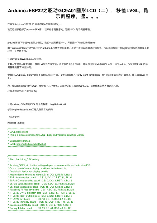
我修改的地⽅(红⾊箭头所指):1. 跑arduino GFX库的LVGL的⽰例程序,LvglHelloWorld修改LvglHelloWorld.ino⼯程⽂件的三处代码:代码源⽂件:#include <lvgl.h>/******************************************************************************** LVGL Hello World* This is a simple examplle for LVGL - Light and Versatile Graphics Library** Dependent libraries:* LVGL: https:///lvgl/lvgl.git******************************************************************************//******************************************************************************** Start of Arduino_GFX setting** Arduino_GFX try to find the settings depends on selected board in Arduino IDE* Or you can define the display dev kit not in the board list* Defalult pin list for non display dev kit:* Arduino Nano, Micro and more: CS: 9, DC: 8, RST: 7, BL: 6* ESP32 various dev board : CS: 5, DC: 27, RST: 33, BL: 22* ESP32-C3 various dev board : CS: 7, DC: 2, RST: 1, BL: 3* ESP32-S2 various dev board : CS: 34, DC: 26, RST: 33, BL: 21* ESP8266 various dev board : CS: 15, DC: 4, RST: 2, BL: 5* Raspberry Pi Pico dev board : CS: 17, DC: 27, RST: 26, BL: 28* RTL8720 BW16 old patch core : CS: 18, DC: 17, RST: 2, BL: 23* RTL8720_BW16 Official core : CS: 9, DC: 8, RST: 6, BL: 3* RTL8722 dev board : CS: 18, DC: 17, RST: 22, BL: 23* RTL8722_mini dev board : CS: 12, DC: 14, RST: 15, BL: 13* Seeeduino XIAO dev board : CS: 3, DC: 2, RST: 1, BL: 0* Teensy 4.1 dev board : CS: 39, DC: 41, RST: 40, BL: 22******************************************************************************/#include <Arduino_GFX_Library.h>/* More dev device declaration: https:///moononournation/Arduino_GFX/wiki/Dev-Device-Declaration*/#if defined(DISPLAY_DEV_KIT)Arduino_GFX *gfx = create_default_Arduino_GFX();#else /* !defined(DISPLAY_DEV_KIT) *//* More data bus class: https:///moononournation/Arduino_GFX/wiki/Data-Bus-Class*///Arduino_DataBus *bus = create_default_Arduino_DataBus();Arduino_DataBus *bus = new Arduino_ESP32SPI(12/* DC */, 15/* CS */, 14/* SCK */, 13/* MOSI */, -1/* MISO */, HSPI /* spi_num */); /* More display class: https:///moononournation/Arduino_GFX/wiki/Display-Class*///Arduino_GFX *gfx = new Arduino_ILI9341(bus, DF_GFX_RST, 0 /* rotation */, false /* IPS */);Arduino_GFX *gfx = new Arduino_GC9A01(bus, 2/* RST */, 0/* rotation */, true/* IPS */);#endif /* !defined(DISPLAY_DEV_KIT) *//******************************************************************************** End of Arduino_GFX setting******************************************************************************/#define DF_GFX_BL 16/* Change to your screen resolution */static uint32_t screenWidth;static uint32_t screenHeight;static lv_disp_draw_buf_t draw_buf;static lv_color_t *disp_draw_buf;static lv_disp_drv_t disp_drv;/* Display flushing */void my_disp_flush(lv_disp_drv_t *disp, const lv_area_t *area, lv_color_t *color_p){uint32_t w = (area->x2 - area->x1 + 1);uint32_t h = (area->y2 - area->y1 + 1);gfx->draw16bitBeRGBBitmap(area->x1, area->y1, (uint16_t *)&color_p->full, w, h);lv_disp_flush_ready(disp);}void setup(){Serial.begin(115200);// while (!Serial);Serial.println("LVGL Hello World");// Init Displaygfx->begin();gfx->fillScreen(BLACK);#ifdef DF_GFX_BLpinMode(DF_GFX_BL, OUTPUT);digitalWrite(DF_GFX_BL, HIGH);delay(100);#endiflv_init();screenWidth = gfx->width();screenHeight = gfx->height();disp_draw_buf = (lv_color_t *)malloc(sizeof(lv_color_t) * screenWidth * 10);if (!disp_draw_buf){Serial.println("LVGL disp_draw_buf allocate failed!");}else{lv_disp_draw_buf_init(&draw_buf, disp_draw_buf, NULL, screenWidth * 10);/* Initialize the display */lv_disp_drv_init(&disp_drv);/* Change the following line to your display resolution */disp_drv.hor_res = screenWidth;disp_drv.ver_res = screenHeight;disp_drv.flush_cb = my_disp_flush;disp_drv.draw_buf = &draw_buf;lv_disp_drv_register(&disp_drv);/* Initialize the (dummy) input device driver */static lv_indev_drv_t indev_drv;lv_indev_drv_init(&indev_drv);indev_drv.type = LV_INDEV_TYPE_POINTER;lv_indev_drv_register(&indev_drv);/* Create simple label */lv_obj_t *label = lv_label_create(lv_scr_act());lv_label_set_text(label, "Arduino-Niceday");lv_obj_align(label, LV_ALIGN_CENTER, 0, 0);Serial.println("Setup done");}}void loop(){lv_timer_handler(); /* let the GUI do its work */delay(5);}烧录代码后的实验效果2.跑lvgl库⾃⾝提供的⽰例代码lvgl⾃⾝提供了很多的example,⽐arduino GFX库的LVGL的⽰例程序要丰富得多,所以我们需要把lvgl⾃⾝提供的⽰例程序跑起来,这样才更有利于学习lvgl。
MiniGUI图形界面实验

学习移植 MiniGUI-STR(for uC/OS-II)软件到 SmartARM2200 开发板的基本方法,然后 编写一个简单的 MiniGUI 应用程序,使用 MessageBox 函数创建一个消息框,消息框中显示 字符串“Hello MiniGUI!” 。 4. 实验预习要求 (1) 仔细阅读<<ARM 嵌入式系统实验教程(二)>>第 1 章的内容,了解 SmartARM2200 开发板的硬件结构,注意 TFT 液晶接口电路和键盘电路。 (2) 阅读 MiniGUI 的文档 <<MiniGUI 用户手册 >> 和 <<MiniGUI 编程指南 >> ,了解 MiniGUI 的基本特点和应用配置选项,以及应用程序的编写。 5. 实验原理 (1) MiniGUI 简介 MiniGUI 项目的最初目标是为基于 Linux 的实时嵌入式操作系统提供一个轻量级的图形 用户界面支持系统,发展到今天,MiniGUI 已进入成熟和稳定阶段,并且所支持的操作系统 已不仅仅限于 Linux,它还可以在 uClinux、uC/OS-II、eCos、VxWorks 等系统上运行。 MiniGUI 为应用程序定义了一组轻量级的窗口和图形设备接口, 利用这些接口, 每个应 用程序可以建立多个主窗口,然后在这些主窗口中创建按钮、编辑框等控制。MiniGUI 还为 用户提供了丰富的图形功能,以显示各种格式的位图并在窗口中绘制复杂图形。 MiniGUI 和嵌入式操作系统的关系如图 1.1 所示,基于 MiniGUI 的应用程序一般通过 ANSI C 库以及 MiniGUI 自身提供的 API 来实现自己的功能。
4
广州周立功单片机发展有限公司 }
Tel: (020)38730976
Atmel ATxmega128A1U 64A1U迁移指南说明书

Atmel AVR1019: Migration fromATxmega128A1/64A1 to ATxmega1281U/64A1UFeatures• Enhancements and added functions • Reset sources • I/O ports• DAC – digital to analog converter •AC – analog comparator1 IntroductionThis application note is a guide to assist users of ATxmega128A1/64A1 in converting designs to Atmel ATxmega128A1U/64A1U. For complete device details, always refer to the most recent version of the ATxmega128A1U/64A1U datasheet and the Atmel ® AVR ® XMEGA ® AU manual. Errata differences between ATxmega128A1/64A1 and ATxmega128A1U/64A1U are not listed in this document, only in the device datasheet.In addition to the differences described in this document, other typical characteristics could be different. Please check the latest datasheet for details. ATxmega128A1U/64A1U also includes new configuration options and functions. As far as possible these are implemented as a superset of existing ATxmega128A1/64A1 functions, so existing code for these devices will work on the new devices without changing existing configuration or enabling new functions. The new options and functions are listed in the application note for customers who in addition to a pure migration also wish to see an overview to consider use of the new functions.8-bit AtmelMicrocontrollersApplication NoteRev. 8415A-AVR-07/112Atmel AVR10198415A-AVR-07/112 Enhancements and added functionsIn this section, we summarize the enhancements or added features in Atmel ATxmega128A1U/64A1U compared with Atmel ATxmega128A1/64A1. For pure migration, you can skip the section and start from the next section.2.1 USB• One USB 2.0 full speed (12Mbps) and low speed (1.5Mbps) device compliant interface is added2.2 Clock system• A divide-by-two option for the PLL output that enables output frequency down to 10MHz• PLL lock failure detection with optionally Non-Maskable Interrupt (NMI), for improved safety and robustness• Non-prescaled Real Time Counter clock source options: External clock from TOSC1, 32.768kHz from TOSC, and the 32.768kHz from the 32.768kHz Internal Oscillator• The 32MHz Internal Oscillator can be tuned to run at any frequency between 30MHz and 55MHz2.3 I/O ports• Alternate pin locations for Timer/Counter 0 Compare Channels, USART0 and SPI • Alternate pin locations for the Peripheral Clock and Event output functions2.4 Analog to digital converter• Automatic input channel scan • VCC/2 voltage reference option• 1/2x (divide by two) gain stage setting•Internal ground can be used as negative input in differential mode (with gain)2.5 Analog comparator• A constant current source2.6 CRC16/CRC32 generator• A CRC16/CRC32 Generator Module that supports CRC16 (RC-CCITT) and CRC-32 (IEEE 802.3)2.7 16-bit timer/counter0• Split mode that enable two 8-bit Timer/Counters with 4PWM channels each2.8 High resolution extension• Hi-Res+ option to allow PWM resolution to be increased with 8x (3-bit)Atmel AVR10193 8415A-AVR-07/112.9 Power management•Possibility to enable sequential start of the components used for analog modulesADC and Analog Comparator in order to reduce start-up current4Atmel AVR10198415A-AVR-07/113 Reset sources3.1 Brown-out detectionThe programmable BODLEVEL settings are different in Atmel ATxmega128A1U/64A1U. See Table 3-1 below for details. Please refer to the device datasheet regarding tolerance for the Brown-out levels. Table 3-1. Brown-out levels.BODLEVELVBOT – XMEGA AUVBOT – XMEGA A111 1.6V 1.6V 110 1.8V 1.9V 101 2.0V 2.1V 011 2.4V 2.6V 010 2.6V 2.9V 000 3.0V 3.4VAtmel AVR10195 8415A-AVR-07/114 I/O portsThe I/O port pins are LVTTL and LVCMOS compatible for AtmelATxmega128A1U/64A1U devices. The minimum “Input High Voltage” is never higherthan 2.0V for VCC > 2.7V.In Atmel ATxmega128A1/64A1, the minimum “Input High Voltage” is 0.7VCC, andcould be higher than 2.0V for VCC>2.86V.6Atmel AVR10198415A-AVR-07/115 DAC – digital to analog converterThe Atmel ATxmega128A1U/64A1U DAC has two continuous output channels, and not a sample and hold circuit as Atmel ATxmega128A1/64A1 devices. This gives continuous time output and higher sample rate for each channel. There is separate calibration (offset/gain) for each DAC channel in ATxmega128A1U/64A1U.When DACA0OFFCAL (in Production Signature Row) is written to CH0OFFSETCAL in DACA, CH1OFFSETCAL is also written with this value. The details of this operation are shown below. The first step,• read DACA0OFFCAL from production signature row • write DACA0OFFCAL to DACA.CH0OFFSETCAL This will result in:• DACA.CH0OFFSETCAL = DACA0OFFCAL • DACA.CH1OFFSETCAL = DACA0OFFCAL The second step,• read DACA1OFFCAL from production signature row • write DACA1OFFCAL to DACA.CH1OFFSETCAL This will result in:• DACA.CH1OFFSETCAL = DACA1OFFCALAfter that, any further writing to DACA.CH0OFFSELCAL does not change DACA.CH1OFFSELCAL until the next reset. The same is implemented for both OFFSET and GAIN calibration registers in DACA and DACB. This ensure that customers using the ATxmega128A1/64A1 DAC can continue and use the same calibration sequence and still calibrate both channels.TIMCTRL register does not exist in ATxmega128A1U/64A1U, so there are no timing constraints on DAC operation.Atmel AVR10197 8415A-AVR-07/116 AC – analog comparatorIn Atmel ATxmega128A1U/64A1U, there is a two-cycle delay from writing a new MUXsetting until it takes effect.8Atmel AVR10198415A-AVR-07/117 Registers7.1 Removed registers and bitsThe below table lists register bits, which exist in Atmel ATxmega128A1/64A1 but not in Atmel ATxmega128A1U/64A1U.Table 7-1. Register bits and functionality that does not exist in ATxmega128A1U/64A1U.Register nameRegister bit FunctionFUSEBYTE2 BODACT[1:0](1)BOD functionality when in active mode CONINTVAL[2:0]DAC Conversion IntervalTIMCTRL REFRESH[3:0]DAC Channel Refresh Timing ControlNote:1. BODACT fuses are now located in FUSEBYTE5 for all devices.Atmel AVR10199 8415A-AVR-07/118 Table of contentsFeatures (1)1 Introduction (1)2 Enhancements and added functions (2)2.1 USB (2)2.2 Clock system (2)2.3 I/O ports (2)2.4 Analog to digital converter (2)2.5 Analog comparator (2)2.6 CRC16/CRC32 generator (2)2.7 16-bit timer/counter0 (2)2.8 High resolution extension (2)2.9 Power management (3)3 Reset sources (4)3.1 Brown-out detection (4)4 I/O ports (5)5 DAC – digital to analog converter (6)6 AC – analog comparator (7)7 Registers (8)7.1 Removed registers and bits (8)8 Table of contents (9)8415A-AVR-07/11Atmel Corporation 2325 Orchard Parkway San Jose, CA 95131 USATel: (+1)(408) 441-0311 Fax: (+1)(408) 487-2600 Atmel Asia Limited Unit 01-5 & 16, 19FBEA Tower, Milennium City 5 418 Kwun Tong Road Kwun Tong, Kowloon HONG KONGTel: (+852) 2245-6100 Fax: (+852) 2722-1369Atmel Munich GmbH Business Campus Parkring 4D-85748 Garching b. Munich GERMANYTel: (+49) 89-31970-0 Fax: (+49) 89-3194621Atmel Japan9F, Tonetsu Shinkawa Bldg. 1-24-8 ShinkawaChou-ku, Tokyo 104-0033 JAPANTel: (+81) 3523-3551 Fax: (+81) 3523-7581© 2011 Atmel Corporation. All rights reserved .Atmel ®, Atmel logo and combinations thereof, AVR ®, XMEGA ®, and others are registered trademarks or trademarks of Atmel Corporation or its subsidiaries. Other terms and product names may be trademarks of others.Disclaimer: The information in this document is provided in connection with Atmel products. No license, express or implied, by estoppel or otherwise, to any intellectual property right is granted by this document or in connection with the sale of Atmel products. EXCEPT AS SET FORTH IN THE ATMEL TERMS AND CONDITIONS OF SALES LOCATED ON THE ATMEL WEBSITE, ATMEL ASSUMES NO LIABILITY WHATSOEVER AND DISCLAIMS ANY EXPRESS, IMPLIED OR STATUTORY WARRANTY RELATING TO ITS PRODUCTS INCLUDING, BUT NOT LIMITED TO, THE IMPLIED WARRANTY OF MERCHANTABILITY, FITNESS FOR A PARTICULAR PURPOSE, OR NON-INFRINGEMENT. IN NO EVENT SHALL ATMEL BELIABLE FOR ANY DIRECT, INDIRECT, CONSEQUENTIAL, PUNITIVE, SPECIAL OR INCIDENTAL DAMAGES (INCLUDING, WITHOUT LIMITATION, DAMAGES FOR LOSS AND PROFITS, BUSINESS INTERRUPTION, OR LOSS OF INFORMATION) ARISING OUT OF THE USE OR INABILITY TO USE THIS DOCUMENT, EVEN IF ATMEL HAS BEEN ADVISED OF THE POSSIBILITY OF SUCH DAMAGES. Atmel makes no representations or warranties with respect to the accuracy or completeness of the contents of this document and reserves the right to make changes to specifications and product descriptions at any time without notice. Atmel does not make any commitment to update the information contained herein. Unless specifically provided otherwise, Atmel products are not suitable for, and shall not be used in, automotive applications. Atmel products are not intended, authorized, or warranted for use as components in applications intended to support or sustain life.。
tslx

TestStation LX andTestStation 12X Technical Product DescriptiontTestStation LX andTestStation 12XTechnical Product DescriptionCopyright © Teradyne, Inc. 2004. All rights reserved under copyright laws of the United States and other countries. The technical data included herein, excluding computer software documentation, is subject to the LIMITED RIGHTS as set forth in FAR 52.227-15 (JUN 1987) and DFARS 252.227-7015 (JUN 1995). All technical data and computer software documentation contained herein is propri-etary and confidential to Teradyne, Inc. or its licensor. All computer software documentation contained herein is Commercial Com-puter Software Documentation, proprietary to Teradyne, Inc. or its licensor and furnished under limited license only. For solicitations issued by the United States, its agencies or instrumentalities (the "Government") on or after December 1, 1995 and the Department of Defense ("DoD") on or after September 29, 1995, the only rights provided in the Commercial Computer Software Documentation shall be those specified in a license customarily provided to the public by Teradyne, Inc. in accordance with FAR 12.212(a) and (b) (OCT 1995) or DFARS 227.7202-3(a) (JUN 1995). For solicitations issued before December 1, 1995 by the Government (other than DoD) use, duplication or disclosure of the documentation shall be subject to the RESTRICTED RIGHTS as set forth in subparagraph (c)(1) and (2) of the commercial computer software - restricted rights clause at FAR 52.227-19 (JUN 1987). For solicitations issued before September 29, 1995 by DoD: RESTRICTED RIGHTS LEGEND - The use, duplication, or disclosure by the Government is subject to restrictions as set forth in subparagraph (c)(1)(ii) of the Rights in Technical Data and Computer Software clause at DFARS 252.227-7013 (OCT 1988).The following are trademarks or registered trademarks of Teradyne, Inc.Product names listed are trademarks of their respective manufacturers. Company names listed are trademarks or trade names of their respective companies.The material in this manual is for informational purposes only and is subject to change, without notice. Teradyne assumes no respon-sibility for any error or for consequential damages that may result from the use or misinterpretation of any of the procedures in this publication.Access Analyzer™Ai-7 Series™Alchemist™APC™Argo™ATG XPRESS™AutoChecker™Autogen™AutoLoad™Autopub™Autotune™BasicSCAN™Bi4-Series™Bi-420™Boundary In-Circuit Test (BICT)™Boundary Scan Intelligent Diagnostics (BSID)™BusBust™BusScan™Call Sentinel™Cap Xpress™CapScan™CASTOR™CatSystem™CCU™Configural Recognition™CMU™Cshell™Component Designer (CDES)™D2B™Design-to-Build™D2B Alchemist™D2B DesignView™D2B ECO™D2B Strategist™D2B DFx™D-TRACKER™DBIU™Defect Display Station (DDS)™DeltaScan™Diamon™DigiBridge™DRMU™EJB-Tester™EJB-Monitor™EJB-Load™EJB-TestSuite™EKB-Test™E-MANAGER™E-SENTINEL™ENCOMPASS™FAST™FrameScan™FrameScan Plus™GENEVA®GenRad®GenRad CAT System™GR®GR-X90™GR-X130™GR-X130L™GR-X160L™GR-X1002™GR-X1500™GR-X1510™GR-X1525™GR-X1550™GR-X4005™GR-X4010™GR-X4011™GR-X7005™GR-X7010™GR2000™ GR4000™GR5000™GR 228X™GR & Des. ™GR AccelerATE®GR Advise™GR Navigate™GRNet™GR Producibility Analyzer™GR Stinger™GR SwitchManager™GR TestManager™GR TestStation™GR TestStation 12X™GR TestStation TSM™GR Versa™GR Versa OT™GR Xpert™GR X-Station 2D™GR X-Station 3-D™GridScan™Inline Device Programmer (ILDP) ™InterScan™Isolution™JUDGE™Junction Xpress™LASAR™L-Series™L200-Series™L300-Series™Lightning™M9-Series™MicroModal™Momentum™MultiScan™MultiScan II™Multi-Tester plus™NIM™NXR™Opens Xpress™Orient Xpress™Panel-Test™PinPoint™PRISM™Production Solutions International™Process Quality Manager™ProcessWatch™ProgramGuide™Program Xplorer™PrompTest™PXIscan™Quick-Check™QuickScan™RCU™RMU™SAC™Safecracker™SafeTest™Scan Pathfinder™Scavenger™Scot™ScratchProbe™SierraMate™SIMUL™Softbridge™Softbridge & Des.™ SoftProbe™Spectrum™Spectrum 8800-Series™SpeedPlus™Stinger™Stronghold™Syncload™The Technology of Knowledge®Teracode™Teradyne®TeraNet™Teradyne & Des. ™TestAdvisor™TestStudio™Test Toolbox™TEST XPRESS™TestLink™Testnet™TPS Converter Studio™TRACS™Vector Bus™Vector Performance (VP)™VICTORY™Virtual In-Circuit Test (VICT)™Virtual Component and Cluster Test (VCCT)™VRS™VXIscan®WaveScan™XFrame™XLT™Xpress Model™Xpress Start™Xpress Train™Xpress Transfer™Xpress Yield™XStation™XStation Combo™XStation HS™Z1800VP™Z1800-Series™Z1820VP™Z1840VP™Z1850VP™Z1880VP™Z1890VP™WARNINGS•Do not remove covers. Potentially lethal voltages are present inside the system. Observe all WARNING markings on the equipment and WARNING notices in the manual. If servicing is necessary, it should be performed only by a qualified person familiar with the electrical shock hazards present inside the system.•Grounding circuit continuity is vital for safe operation of the equipment. Never operate equipment with grounding conductor disconnected.•Safeguard your hands and fingers while handling any fixture or other accessory. Be sure it is securely supported if you reach under it. If it is heavy, you must have another person help to move it.•The symbol on equipment signifies that the manual contains information to prevent injury or equipment damage. Observe and heed all WARNING notices in the manuals and the equipment. WARNINGS call attention to personnel safety information.•Replace any fuse only with the same type and ratings as labeled on the equipment and/or listed in the manual.MISES EN GARDE•Ne pas enlever les couvercles. Les niveaux de tension se trouvant dans le système sont extrêmement dangereux. Respectez toutes les consignes de sécurité figurant sur l'équipement et les MISES EN GARDE données dan ce manuel. Seule une personne qualifée, connaisant les risques de décharge électrique du système, est autorisée à effecteur les opérations de nettoyage ou de réparation du système.•Le circuit doit être mis à la terre sans discontinuation pour garantir un fonctionnement sans danger de l'équipement. Ne jamais faire fonctionner l'équipement pendant que le raccord à la terre est déconnecté.•Protégez-vous les mains et les doigts pendant le maniement de tout dispositif de serrage ou autre accessoire.Assurez-vous que ceux-ci soient bien solidement fixés en place, avant de vous pencher sous eux. Si l'accessoire en question est trop lourd, faites-vous aider pour le déplacer.•Le symbole figurant sur l'équipement signifie que le manuel contient des informations permettant d'empêcher les accidents ou l'endommagement de l'équipement. Respectez toutes les consignes de MISES EN GARDE données dans le manuel et figurant sur l'équipement. Les MISES EN GARDE attirent l'attention sur la nécessité de se protéger.•Ne remplacez les fusibles qu'avec des fusibles du même type et de la même valuer que ceux mentionnés sur l'équipement et figurant dans le manuel.WARNHINWEISE•Abdeckungen nicht entfernen. Potentiell lebensgefährliche Spannungsbedingungen innerhalb des Systems vorhanden. Alle auf der Einrichtung befindlichen WARNMARKIERUNGEN und im Handbuch enthaltenen WARNHINWEISE beachten. Wartungsarbeiten dem qualifizierten Personal überlassen, das mit den innerhalb des Systems vorhandenen Gefahren eines elektrischen Schlags vertraut ist.•Die Erdung des Schaltungsdurchgangs ist eine Grundvoraussetzung für den sicheren Betrieb der Einrichtung.Einrichtung niemals ohne Erdleiter betreiben.•Hände und Finger bei der Handhabung einer Spannvorrichtung oder eines anderen Zubehörteils schützen.Sich vor der Plazierung der Hände unterhalb der Einrichtung vergewissern, daß die Einrichtung über ausreichenden Halt verfügt. Falls die Einrichtung schwer ist, sich von einer anderen Person beim Tragen helfen lassen.•Das auf der Einrichtung befindliche Symbol bedeutet, daß das Handbuch Informationen zur Verhinderung von Körperverletzungen oder Sachschäden enthält. Alle in den Handbüchern enthaltenen und auf der Einrichtung befindlichen WARNHINWEISE beachten und befolgen. WARNHINWEISE sollen auf Informationen zur persönlichen Sicherheit aufmerksam machen.•Sicherungen nur durch Sicherungen des gleichen Typs und der gleichen Nennleistung ersetzen. Auf der Einrichtung befindliche Etiketten und im Handbuch enthaltene Informationen zu Rate ziehen.!IEC417!IEC417!IEC417AVISOS•Não remova as tampas. Há voltagens potencialmente fatais presentes na parte interna do sistema. Observe todas as marcações de AVISOS no equipamento e discrições de AVISOS no manual. Se for necessário fazer manutenção, esta deve ser feita somente por uma pessoa qualificada familiarizada com os perigos de choques elétricos presentes na parte interna do sistema.• A continuidade do circuito de aterramento é vital para a operação segura do equipamento. Nunca opere o equipamento com o cabo de aterramento desligado.•Proteja as suas mãos e dedos ao operar qualquer dispositivo ou outro acessório. Certifique-se que ele esteja suportado com segurança se você tiver que alcançar algo debaixo dele. Se for pesado, você deve ter a ajuda de uma outra pessoa para movê-lo.•O simbolo no equipamento significa que o manual contém informações para prevenir ferimentos ou danos ao equipamento. Observe e preste atenção a todos os AVISOS nos manuais e no equipamento.Os AVISOS chamam a atenção a informações sobre a segurança pessoal.•Substitua qualquer fusivel somente com um do mesmo tipo e da mesma capacidade nominal como marcado no equipamento e listado no manual.ADVERTENCIAS•No quitar las tapas. En el interno del sistema hay voltajes potencialmente mortales. Obsérvense todos los rótulos de ADVERTENCIA presentes en el equipo, así como la descripción de las notas de ADVERTENCIA presentadas en el manual. De ser necesario, el servicio de mantenimiento deberá ser efectuado únicamente por personal calificado que esté familiarizado con los peligros de choque eléctrico presentes en el sistema.•La continuidad del circuito de puesta a tierra es de vital importancia para el functionamiento seguro del equipo.Nunca se debe usar el equipo con el conductor de puesta a tierra desconectado.•Protéjanse las manos y los dedos toda vez que sea necesario manipular un dispositivo u accesorio.Cerciorarse de que el mismo esté firmemente sujetado antes de proceder a trabajar debajo de él. Si el aparato u accesorio fuera pesado, pedir la ayuda de otra persona para moverlo.•El simbolo que aparece en el equipo significa que el manual contiene informaciones para evitar lesiones personales o daños al equipo. Obsérvense y préstese atención a toda las notas de ADVERTENCIA presentes en los manuales y en el equipo. Las ADVERTENCIAS sirven para llamar la atención sobre informaciones de seguridad para el personal.•Reemplazar los fusibles únicamente con otros del mismo tipo y capacidad, según lo indique el rótulo en el equipo y la descripción en el manual.CAUTIONS•Observe and heed all CAUTION notices in the manuals and on the equipment. CAUTIONS call attention to information about safeguarding equipment from damage.!IEC417!IEC417HANDLING PRECAUTIONS FOR ELECTRONIC DEVICES SUBJECT TO DAMAGE BY STATIC ELECTRICITYPlace instrument or module to be serviced, spare parts in conductive (anti-static) envelopes or carriers, hand tools etc. on a work surface defined as follows. The work surface must be conductive and reliably connected to earth ground through a safety resistance of approximately 250 kilohms. The sur-face must NOT be metal. (A resistivity of 30 to 300 kilohms per square inch is suggested.) Avoid placing tools or electri-cal parts on insulators.Ground the frame of any line-powered equipment, test instru-ments, lamps, soldering irons, etc., directly to earth ground. To avoid shorting out the safety resistance, be sure that grounded equipment has rubber feet or other means of insu-lation from the work surface. The module being serviced should be insulated while grounded through the power-cord ground wire, but must be connected to the work surface before, during and after any disassembly or other procedure in which the line cord is disconnected.Exclude any hand tools (such as non-conductive plunger-type solder suckers) that can generate a static charge.Ground yourself reliably, through a resistance, to the work surface; use, for example, a conductive strap or cable with a wrist cuff. The cuff must make electrical contact directly with your skin; do NOT wear it over clothing. (Resistance between skin contact and work surface through a commer-cially available personnel grounding device is typically 250 kilohms to 1 megohm.)If any circuit or IC packages are to be stored or transported, enclose them in conductive envelopes or carriers. Remove them only with the above precautions; handle IC packages without touching the contact pins.Avoid circumstances that are likely to produce static charges, such as wearing clothes of synthetic material, sitting on a plastic-covered stool (particularly while wearing wool), comb-ing your hair, or making extensive erasures. These circum-stances are most significant when the air is dry.When testing static sensitive devices, be sure DC power is on before, during, and after application of test signals. Be sure all pertinent voltages have been switched off while boards orcomponents are removed or inserted.ContentsUsing This ManualOverview . . . . . . . . . . . . . . . . . . . . . . . . . . . . . . . . . . . . . . . . . . . . . . . . . . . . . . . . . . . . . . . . . . . . . . xi Technical Support Center . . . . . . . . . . . . . . . . . . . . . . . . . . . . . . . . . . . . . . . . . . . . . . . . . . . . . . . . . xi How To Order Additional Documentation. . . . . . . . . . . . . . . . . . . . . . . . . . . . . . . . . . . . . . . . . . . . . . xii Patent Information . . . . . . . . . . . . . . . . . . . . . . . . . . . . . . . . . . . . . . . . . . . . . . . . . . . . . . . . . . . . . . . xiiIntroductionIntroduction . . . . . . . . . . . . . . . . . . . . . . . . . . . . . . . . . . . . . . . . . . . . . . . . . . . . . . . . . . . . . . . . . . .1 - 1 Standard System Configuration. . . . . . . . . . . . . . . . . . . . . . . . . . . . . . . . . . . . . . . . . . . . . . . . . . . .1 - 3 System Software . . . . . . . . . . . . . . . . . . . . . . . . . . . . . . . . . . . . . . . . . . . . . . . . . . . . . . . . . . .1 - 3 Test Hardware . . . . . . . . . . . . . . . . . . . . . . . . . . . . . . . . . . . . . . . . . . . . . . . . . . . . . . . . . . . . .1 - 4 Computer and Peripherals . . . . . . . . . . . . . . . . . . . . . . . . . . . . . . . . . . . . . . . . . . . . . . . . . . . .1 - 6 Service and Support . . . . . . . . . . . . . . . . . . . . . . . . . . . . . . . . . . . . . . . . . . . . . . . . . . . . . . . . .1 - 6 Optional System Software . . . . . . . . . . . . . . . . . . . . . . . . . . . . . . . . . . . . . . . . . . . . . . . . . . . . . . . .1 - 6 Optional System Hardware . . . . . . . . . . . . . . . . . . . . . . . . . . . . . . . . . . . . . . . . . . . . . . . . . . . . . . .1 - 7 Optional Computer Peripherals . . . . . . . . . . . . . . . . . . . . . . . . . . . . . . . . . . . . . . . . . . . . . . . . . . . .1 - 8 Overview of Software Licenses . . . . . . . . . . . . . . . . . . . . . . . . . . . . . . . . . . . . . . . . . . . . . . . . . . . .1 - 8Analog SubsystemOverview . . . . . . . . . . . . . . . . . . . . . . . . . . . . . . . . . . . . . . . . . . . . . . . . . . . . . . . . . . . . . . . . . . . . .2 - 1 Instrumentation . . . . . . . . . . . . . . . . . . . . . . . . . . . . . . . . . . . . . . . . . . . . . . . . . . . . . . . . . . . . . . . .2 - 2 ICA Module . . . . . . . . . . . . . . . . . . . . . . . . . . . . . . . . . . . . . . . . . . . . . . . . . . . . . . . . . . . . . . . .2 - 2 Digital Voltmeter (DVM) . . . . . . . . . . . . . . . . . . . . . . . . . . . . . . . . . . . . . . . . . . . . . . . . . . . . . .2 - 3 AC and DC Current Measure . . . . . . . . . . . . . . . . . . . . . . . . . . . . . . . . . . . . . . . . . . . . . . . . . .2 - 3 DC/AC Source Amplifiers . . . . . . . . . . . . . . . . . . . . . . . . . . . . . . . . . . . . . . . . . . . . . . . . . . . . .2 - 3 Impedance Measurement . . . . . . . . . . . . . . . . . . . . . . . . . . . . . . . . . . . . . . . . . . . . . . . . . . . . .2 - 4 Arbitrary Waveform Generator (AWG) . . . . . . . . . . . . . . . . . . . . . . . . . . . . . . . . . . . . . . . . . . .2 - 4 Digital Multimeter (DMM) . . . . . . . . . . . . . . . . . . . . . . . . . . . . . . . . . . . . . . . . . . . . . . . . . . . . .2 - 5 ICA Controls, Triggers, and Timers . . . . . . . . . . . . . . . . . . . . . . . . . . . . . . . . . . . . . . . . . . . . .2 - 5 ICA Instrument Multiplexer . . . . . . . . . . . . . . . . . . . . . . . . . . . . . . . . . . . . . . . . . . . . . . . . . . . .2 - 6 High Voltage Source . . . . . . . . . . . . . . . . . . . . . . . . . . . . . . . . . . . . . . . . . . . . . . . . . . . . . . . . .2 - 6 Calibration Daughter Board . . . . . . . . . . . . . . . . . . . . . . . . . . . . . . . . . . . . . . . . . . . . . . . . . . .2 - 6 Self-Test Circuits . . . . . . . . . . . . . . . . . . . . . . . . . . . . . . . . . . . . . . . . . . . . . . . . . . . . . . . . . . .2 - 6 IEEE-488 Multiplexer . . . . . . . . . . . . . . . . . . . . . . . . . . . . . . . . . . . . . . . . . . . . . . . . . . . . . . . .2 - 7ContentsRelay-Driver Function . . . . . . . . . . . . . . . . . . . . . . . . . . . . . . . . . . . . . . . . . . . . . . . . . . . . . . . .2 - 7 ICA Specifications . . . . . . . . . . . . . . . . . . . . . . . . . . . . . . . . . . . . . . . . . . . . . . . . . . . . . . . . . .2 - 8 High Voltage Source . . . . . . . . . . . . . . . . . . . . . . . . . . . . . . . . . . . . . . . . . . . . . . . . . . . . . . . .2 - 11 AWG Source . . . . . . . . . . . . . . . . . . . . . . . . . . . . . . . . . . . . . . . . . . . . . . . . . . . . . . . . . . . . . .2 - 14 Scanner Switching Matrix. . . . . . . . . . . . . . . . . . . . . . . . . . . . . . . . . . . . . . . . . . . . . . . . . . . . . . . .2 - 16 Switching Matrix Specifications . . . . . . . . . . . . . . . . . . . . . . . . . . . . . . . . . . . . . . . . . . . . . . .2 - 20 Measurement Methods and Specifications . . . . . . . . . . . . . . . . . . . . . . . . . . . . . . . . . . . . . . . . . .2 - 22 UUT Shorts Test . . . . . . . . . . . . . . . . . . . . . . . . . . . . . . . . . . . . . . . . . . . . . . . . . . . . . . . . . . .2 - 22 Opens Test . . . . . . . . . . . . . . . . . . . . . . . . . . . . . . . . . . . . . . . . . . . . . . . . . . . . . . . . . . . . . . .2 - 22 Capacitive Tests . . . . . . . . . . . . . . . . . . . . . . . . . . . . . . . . . . . . . . . . . . . . . . . . . . . . . . . . . . .2 - 23 Junction Xpress . . . . . . . . . . . . . . . . . . . . . . . . . . . . . . . . . . . . . . . . . . . . . . . . . . . . . . . . . . .2 - 25 Resistance Measurements . . . . . . . . . . . . . . . . . . . . . . . . . . . . . . . . . . . . . . . . . . . . . . . . . . .2 - 25 Impedance Measurements . . . . . . . . . . . . . . . . . . . . . . . . . . . . . . . . . . . . . . . . . . . . . . . . . . .2 - 32 AC Resistance . . . . . . . . . . . . . . . . . . . . . . . . . . . . . . . . . . . . . . . . . . . . . . . . . . . . . . . . . . . .2 - 32 Capacitance Test . . . . . . . . . . . . . . . . . . . . . . . . . . . . . . . . . . . . . . . . . . . . . . . . . . . . . . . . . .2 - 33 Inductance Test Procedures . . . . . . . . . . . . . . . . . . . . . . . . . . . . . . . . . . . . . . . . . . . . . . . . . .2 - 35 6-Wire AC Measurement . . . . . . . . . . . . . . . . . . . . . . . . . . . . . . . . . . . . . . . . . . . . . . . . . . . .2 - 36 Diode Test . . . . . . . . . . . . . . . . . . . . . . . . . . . . . . . . . . . . . . . . . . . . . . . . . . . . . . . . . . . . . . .2 - 37 Transistor Test. . . . . . . . . . . . . . . . . . . . . . . . . . . . . . . . . . . . . . . . . . . . . . . . . . . . . . . . . . . . . . . .2 - 38 NPN and PNP Tests . . . . . . . . . . . . . . . . . . . . . . . . . . . . . . . . . . . . . . . . . . . . . . . . . . . . . . . .2 - 38 FET Channel Impedance Test . . . . . . . . . . . . . . . . . . . . . . . . . . . . . . . . . . . . . . . . . . . . . . . .2 - 39 Zener Diode Test . . . . . . . . . . . . . . . . . . . . . . . . . . . . . . . . . . . . . . . . . . . . . . . . . . . . . . . . . .2 - 39 SCR Test . . . . . . . . . . . . . . . . . . . . . . . . . . . . . . . . . . . . . . . . . . . . . . . . . . . . . . . . . . . . . . . .2 - 40 Operational Amplifier Test . . . . . . . . . . . . . . . . . . . . . . . . . . . . . . . . . . . . . . . . . . . . . . . . . . .2 - 41 Analog Functional/Mixed Signal Testing . . . . . . . . . . . . . . . . . . . . . . . . . . . . . . . . . . . . . . . . . . . .2 - 42Digital SubsystemOverview . . . . . . . . . . . . . . . . . . . . . . . . . . . . . . . . . . . . . . . . . . . . . . . . . . . . . . . . . . . . . . . . . . . . .3 - 1 System Controller. . . . . . . . . . . . . . . . . . . . . . . . . . . . . . . . . . . . . . . . . . . . . . . . . . . . . . . . . . . . . . .3 - 2 Controller Functions . . . . . . . . . . . . . . . . . . . . . . . . . . . . . . . . . . . . . . . . . . . . . . . . . . . . . . . . .3 - 2 Clock/Sync/Trigger Logic. . . . . . . . . . . . . . . . . . . . . . . . . . . . . . . . . . . . . . . . . . . . . . . . . . . . . . . . .3 - 3 Timing Specifications for the CST . . . . . . . . . . . . . . . . . . . . . . . . . . . . . . . . . . . . . . . . . . . . . .3 - 4 Clock Drive/Synchronization for the CST . . . . . . . . . . . . . . . . . . . . . . . . . . . . . . . . . . . . . . . . .3 - 4 Trigger Pins for the CST . . . . . . . . . . . . . . . . . . . . . . . . . . . . . . . . . . . . . . . . . . . . . . . . . . . . . .3 - 5 Driver/Sensor Modules. . . . . . . . . . . . . . . . . . . . . . . . . . . . . . . . . . . . . . . . . . . . . . . . . . . . . . . . . . .3 - 6 Driver/Sensor Architecture . . . . . . . . . . . . . . . . . . . . . . . . . . . . . . . . . . . . . . . . . . . . . . . . . . . .3 - 7 Additional Features of Ultra 12X Pin Boards . . . . . . . . . . . . . . . . . . . . . . . . . . . . . . . . . . . . . .3 - 9 SafeTest. . . . . . . . . . . . . . . . . . . . . . . . . . . . . . . . . . . . . . . . . . . . . . . . . . . . . . . . . . . . . . . . . . . . .3 - 10ContentsAutomatic Driver Verification . . . . . . . . . . . . . . . . . . . . . . . . . . . . . . . . . . . . . . . . . . . . . . . . .3 - 10 Real-Time Backdrive Current Measurement Capabilities . . . . . . . . . . . . . . . . . . . . . . . . . . . .3 - 10 Closed Loop, Low Output Impedance Drivers . . . . . . . . . . . . . . . . . . . . . . . . . . . . . . . . . . . .3 - 10 Multi-Level Digital Isolation . . . . . . . . . . . . . . . . . . . . . . . . . . . . . . . . . . . . . . . . . . . . . . . . . . .3 - 10 Per Pin Programmable Logic Level Assignments . . . . . . . . . . . . . . . . . . . . . . . . . . . . . . . . .3 - 10 Programmable Backdrive Currents and Duration . . . . . . . . . . . . . . . . . . . . . . . . . . . . . . . . . .3 - 11 Specialized Digital Controller and Timing . . . . . . . . . . . . . . . . . . . . . . . . . . . . . . . . . . . . . . . .3 - 11Optional Test HardwareOverview . . . . . . . . . . . . . . . . . . . . . . . . . . . . . . . . . . . . . . . . . . . . . . . . . . . . . . . . . . . . . . . . . . . . .4 - 1 Analog Functional Test Module (AFTM) . . . . . . . . . . . . . . . . . . . . . . . . . . . . . . . . . . . . . . . . . . . . .4 - 1 AFTM Specifications . . . . . . . . . . . . . . . . . . . . . . . . . . . . . . . . . . . . . . . . . . . . . . . . . . . . . . . . .4 - 2 DC Voltage Measure . . . . . . . . . . . . . . . . . . . . . . . . . . . . . . . . . . . . . . . . . . . . . . . . . . . . . . . .4 - 2 AC Voltage Measure . . . . . . . . . . . . . . . . . . . . . . . . . . . . . . . . . . . . . . . . . . . . . . . . . . . . . . . .4 - 3 DC Source . . . . . . . . . . . . . . . . . . . . . . . . . . . . . . . . . . . . . . . . . . . . . . . . . . . . . . . . . . . . . . . .4 - 3 AC Source . . . . . . . . . . . . . . . . . . . . . . . . . . . . . . . . . . . . . . . . . . . . . . . . . . . . . . . . . . . . . . . .4 - 4 Sync Source . . . . . . . . . . . . . . . . . . . . . . . . . . . . . . . . . . . . . . . . . . . . . . . . . . . . . . . . . . . . . . .4 - 4 Instrument Multiplexer . . . . . . . . . . . . . . . . . . . . . . . . . . . . . . . . . . . . . . . . . . . . . . . . . . . . . . .4 - 4 Frequency/Time Interval Meter (FTM) . . . . . . . . . . . . . . . . . . . . . . . . . . . . . . . . . . . . . . . . . . .4 - 5 Deep Serial Memory . . . . . . . . . . . . . . . . . . . . . . . . . . . . . . . . . . . . . . . . . . . . . . . . . . . . . . . . . . . .4 - 5 DSM Applications . . . . . . . . . . . . . . . . . . . . . . . . . . . . . . . . . . . . . . . . . . . . . . . . . . . . . . . . . . .4 - 6 Custom Function Board (CFB). . . . . . . . . . . . . . . . . . . . . . . . . . . . . . . . . . . . . . . . . . . . . . . . . . . . .4 - 7 Custom Function Board Applications . . . . . . . . . . . . . . . . . . . . . . . . . . . . . . . . . . . . . . . . . . . .4 - 8 Vehicle Control Interface (VCI) . . . . . . . . . . . . . . . . . . . . . . . . . . . . . . . . . . . . . . . . . . . . . . . . .4 - 8 Frequency/Time Interval Instrument Module (FTI) . . . . . . . . . . . . . . . . . . . . . . . . . . . . . . . . . .4 - 8 FTI Specifications . . . . . . . . . . . . . . . . . . . . . . . . . . . . . . . . . . . . . . . . . . . . . . . . . . . . . . . . . .4 - 9 Duty Cycle . . . . . . . . . . . . . . . . . . . . . . . . . . . . . . . . . . . . . . . . . . . . . . . . . . . . . . . . . . . . . . .4 - 10 System Frequency/Time Meter (SFTM). . . . . . . . . . . . . . . . . . . . . . . . . . . . . . . . . . . . . . . . . . . . .4 - 10Unit Under Test Power SuppliesOverview . . . . . . . . . . . . . . . . . . . . . . . . . . . . . . . . . . . . . . . . . . . . . . . . . . . . . . . . . . . . . . . . . . . . .5 - 1 Programmable Voltage Power Supplies . . . . . . . . . . . . . . . . . . . . . . . . . . . . . . . . . . . . . . . . . . . . .5 - 1 Common Specifications . . . . . . . . . . . . . . . . . . . . . . . . . . . . . . . . . . . . . . . . . . . . . . . . . . . . . .5 - 2 Programmable Power Supply Specifications . . . . . . . . . . . . . . . . . . . . . . . . . . . . . . . . . . . . . .5 - 3 Optional Fixed Voltage Power Supplies. . . . . . . . . . . . . . . . . . . . . . . . . . . . . . . . . . . . . . . . . . . . . .5 - 4System Layout and Mechanical/Industrial SpecificationsSystem Layout. . . . . . . . . . . . . . . . . . . . . . . . . . . . . . . . . . . . . . . . . . . . . . . . . . . . . . . . . . . . . . . . .6 - 1 Power Bay . . . . . . . . . . . . . . . . . . . . . . . . . . . . . . . . . . . . . . . . . . . . . . . . . . . . . . . . . . . . . . . .6 - 1。
S7-200 SMART PLC 系统功能说明(图文并茂)

Page 1 of 58
存储卡
S 7 2 0 0S M A R TC P U支持商用M i c r o S D 卡(支持容量为4 G ,8 G ,1 6 G ):可用于程序传输,C P U 固件更新,恢复 C P U出厂设置。 打开C P U 本体数字量输出点上方的端子盖,可以看到右侧有一卡槽,将M i c r o S D 卡缺口向里插入,如图 1 所示:
S7-200 SMART 实时时钟
S 7 2 0 0S M A R T 的硬件实时时钟可以提供年、月、日、时、分、秒的日期/ 时间数据。 C P UC R 4 0A C / D C / R e l a y没有内置的实时时钟,C P US R 2 0 、C P US R 4 0 、C P US T 4 0 、C P US R 6 0 、C P US T 6 0 支持内置的实时时钟,C P U 断电 状态下可保持7 天。 S 7 2 0 0S M A R TC P US R 2 0 的时钟精度是± 1 2 0秒 /月,C P US R 4 0 、C P US T 4 0 、C P US R 6 0 、C P US T 6 0 的时钟精度是 1 2 0秒 /月。 S 7 2 0 0S M A R TC P U靠内置超级电容为实时时钟提供电源缓冲,保持时间为典型值7 天,最小值6 天。缓冲电源放电完毕后,再次上电后 时钟将停止在缺省值,并不开始走动。 注意:因为 C P UC R 4 0无内置超级电容,所以实时时钟无电源缓冲,尽管用户可以使用R E A D _ R T C和 S E T _ R T C指令设置日期/ 时间 数据,但是当 C P UC R 4 0断电并再次上电时,这些日期/ 时间数据会丢失,上电后日期时间数据会被初始化为2 0 0 0 年1 月1 日。 为了提高运算效率,应当避免每个程序周期都读取实时时钟。实际上可读取的最小时间单位是1 秒,可每秒读取一次(使用S M 0 . 5 上 升沿触发读取指令)。 使用程序读取的实时时钟数据为B C D 格式,可在状态表中使用十六进制格式查看。 要设置日期、时间值,使之开始走动,可以:
如何在matlab中使用NXP MCU的工具箱和数学函数库以及其他调试工具
AMF-ACC-T1114
Mike Doidge | MCD Toolbox Manager John H. Floros | Field Application Engineer
Now that more testing on target has occurred earlier in the process, HIL testing time is reduced.
With MC Toolbox, auto-generate code for direct interface of peripherals for target hardware without any manual hand code.
S E P T. 2 0 1 5
TM
External Use
Agenda
•
Overview: 20 minutes
− −
Introduction and Objectives Motor Control Development Toolbox: Library blocks, FreeMASTER, and Bootloader
TM
External Use
3
Introduction: Motor Control Development Toolbox
•
The Motor Control Development Toolbox includes an embedded target supporting Freescale MCUs and Simulink™ plug-in libraries which provide engineers with an integrated environment and tool chain for configuring and generating the necessary software, including initialization routines, device drivers, and a real-time scheduler to execute algorithms specifically for controlling motors. The toolbox also includes an extensive Automotive Math and Motor Control Function Library developed by Freescale’s renowned Motor Control Center of Excellence. The library provides dozens of blocks optimized for fast execution on Freescale MCUs with bit-accurate results compared to Simulink™ simulation using single -precision math. The toolbox provides built-in support for Software and Processor-in-the-Loop (SIL and PIL), which enables direct comparison and plotting of numerical results. MathWorks products required for MC Toolbox: − MATLAB (32-Bit or 64-Bit)* − Simulink − MATLAB Coder − Simulink Coder − Embedded Coder
STC开发 烧录工具说明
13.2.8 如何解决VB版ISP工具在XP或WIN7下控件过期或不能注册的问题....... 48
南通国芯微电子有限公司
总机:0513-5501 2928 / 2929 / 2966
传真:0513-5501 2969 / 2956 / 2947
STC-ISP下载编程工具使用说明
STC — 8051单片机全球第一品牌,全球最大的8051单片机设计公司
南通国芯微电子有限公司
总机:0513-5501 2928 / 2929 / 2966
传真:0513-5501 2969 / 2956 / 2947
STC-ISP下载编程工具使用说明
STC — 8051单片机全球第一品牌,全球最大的8051单片机设计公司
这样Keil μVision2的设备库中就有了STC型号,如下图所示
13.4 自定义下载及其演示程序(实现不停电下载)................... 65 13.5 若无仿真器,如何调试/开发用户程序........................ 69 13.6 STC15系列仿真器的说明——可以仿真新的STC15系列. ......... 70
C T S
U C M
Li
. d e t i m
更新日期:2012-3-12
南通国芯微电子有限公司
总机:0513-5501 2928 / 2929 / 2966
传真:0513-5501 2969 / 2956 / 2947
STC-ISP下载编程工具使用说明
技术支持网站:
临时技术支持:13922829991
(4)单击保存后会弹出"Select Device for Target"对话框,如下所示,用户需在左侧的数据列 表(Data base)选择所使用的单片机型号,STC单片机可以选择Intel 80/87C58.
STM32到GD32移植攻略
STM32到GD32移植攻略这是一个关于将STM32移植到GD32的攻略,以下是详细步骤:1.硬件适配:首先,了解两个平台的硬件特性和功能差异。
GD32是根据STM32的特性进行优化设计的,硬件接口和外设与STM32非常相似。
然而,仍然需要查阅相关的资料和数据手册,确保GD32的引脚、时钟、外设和内部Flash、SRAM等与原始的STM32设备一致。
2.移植GPIO:GPIO是移植的第一个部分,因为绝大多数应用都需要使用GPIO。
首先查看STM32的GPIO配置与寄存器的对应关系,然后通过修改相关的头文件和函数,将STM32的GPIO库移植到GD32上。
3.移植时钟模块:时钟模块也是移植过程中很重要的一部分。
首先,了解STM32和GD32的时钟配置寄存器和相关的位定义。
然后,根据这些信息修改GD32的时钟初始化函数和头文件,以适配原有的STM32时钟设置。
4.移植外设驱动库:5.调试和测试:移植完成后,进行调试和测试是非常重要的。
使用调试器来验证代码的正确性,确保所有的外设和模块都能按预期工作。
在测试过程中,如果发现有一些不一致或功能缺失,需要回到前面的步骤进行修复,直到移植完成。
6.性能优化和功能扩展:在移植完成后,可以进行性能优化和功能扩展。
根据实际需求,对代码进行优化,提高代码的执行效率和系统的响应速度。
同时,也可以添加一些额外的功能,以满足应用的需求。
总结:移植STM32到GD32需要仔细阅读GD32和STM32的文档、数据手册和外设驱动库,并进行逐步的适配和修改。
在移植过程中,要注意硬件适配、时钟配置、外设驱动和调试测试等方面。
这个攻略提供了大致的步骤和指导,但具体的移植过程还需要根据具体的情况进行调整和优化。
希望这些信息能够对你在将STM32移植到GD32的过程中有所帮助。
互芯移植入门
互芯移植入门注意:以下所有的说明是针对"\\192.168.1.87\sysdev\coolsand(互芯)\工程\《互芯__1131.rar》"来说的,其余工程类似。
服务器上存放互芯相关文件的地址:\\192.168.1.87\sysdev\coolsand\\192.168.1.87\sysdev\coolsand(互芯)\相关资料: coolsand指导文档:《互芯平台GSM软件简明教程.doc》\\192.168.1.87\sysdev\coolsand(互芯)\工程: 为互芯平台工程\\192.168.1.87\sysdev\coolsand(互芯)\环境:为互芯平台安装环境所需的软件\\192.168.1.87\sysdev\coolsand(互芯)\工具:为烧机等工具所有的知识都可以通过学习《互芯平台GSM软件简明教程.doc》掌握。
一、coolsand环境搭建所需文件目录:\\192.168.1.87\sysdev\coolsand(互芯)\环境\1.准备工作:a.[必选]建立一个目录,以后所有的代码均放在该目录下(例如:D:\Cool_prj),里面每个项目的结构形似:XX_PRJ\soft(即D:\Cool_prj\XX_PRJ\soft) [注意,XX_PRJ下面必须是soft!!]b.[可选]建立该工作目录的分区,最好能在域用户登录的情况下,格式化一下(防止有些权限问题)[这步可先不做,如果有权限问题在做也可以]2. 在安装之前,请检查电脑是否已经安装过cygwin,若是请先将以前安装过的cygwin卸载掉。
安装CSDTK3.5_Cygwin1.5.25_Svn_1.5.4_Full_Setup,默认安装即可,全部点NEXT3.运行桌面的Cygwin如果出现以下提示:Your group is currently "mkpasswd". This indicates thatthe /etc/passwd (and possibly /etc/group) files should be rebuilt.See the man pages for mkpasswd and mkgroup then, for example, runmkpasswd -l [-d] > /etc/passwdmkgroup -l [-d] > /etc/groupNote that the -d switch is necessary for domain users.1)分别执行以下2个命令mkpasswd -l -d > /etc/passwdmkgroup -l -d > /etc/group如果均无任何提示,则表示成功,跳过下一步2).如果有失败提示,a.关闭Cygwinb.从已经安装好的机器上拷贝 passwd 和 group文件的域部分(现在为止该问题未知是什么问题)重新打开若不出现提示,则OK4.复制bashrc文件夹内部的4个文件(真正用到的只有3个文件,readme.txt文件是说明文件,用心看吧),粘贴并覆盖到C:\CSDTK\cygwin\home\(用户名)\5.修改默认工作路径:修改C:\CSDTK\cygwin\home\(用户名【一般是Administrator】)\.bashrc内的PROJ_ROOT_WIN的路径,改为自己定义的工作目录(例如:D:\Cool_prj)6.编译代码时,打开Cygwin, 然后输入 work XX_PRJ 切换到工作目录,然后输入编译命令即可编译二、coolsand烧机工具所需文件目录:\\192.168.1.87\sysdev\coolsand(互芯)\工具\烧机工具为类似ProductLineToolV5.00.06_20111013目前下载工具见到的有3个版本,分别是V5.0.6,V6.0.*,V7.0.2。
- 1、下载文档前请自行甄别文档内容的完整性,平台不提供额外的编辑、内容补充、找答案等附加服务。
- 2、"仅部分预览"的文档,不可在线预览部分如存在完整性等问题,可反馈申请退款(可完整预览的文档不适用该条件!)。
- 3、如文档侵犯您的权益,请联系客服反馈,我们会尽快为您处理(人工客服工作时间:9:00-18:30)。
一文详解TI的grlib图形库移植到Atmel SAM4套件
图形库其实都是都是由底层的画点,画线等这些基本函数组成。
大家以前上数学都有学过点成线,线成面这些的,而图形库也是基于此的。
TI的图形库分3层,如下图:
我们只需要修改显示驱动层即可。
上面两层都是在调用最低层的驱动层。
显示驱动层函数要我们重写,不是很多,就只有几个函数而已:
如下截图:
分别是:
画点函数:void PixelDraw(void *pvDisplayData,long x,long y,unsigned longcolor);画多点的函数:void PixelDrawMultiple(void *pvDisplayData,
longx,
longy,
longx0,
longlCount,
longBPP,
constunsigned char *pucData,
constunsigned char *pucPalette)
{
画横线的函数:void LineDrawH (void *pvDisplayData,long x1,long x2,long y,unsigned long color);
画竖线的函数:void LineDrawH (void *pvDisplayData,long x1,long x2,long y,unsigned long color);
矩形填充函数:void RectFill (void *pvDisplayData,const tRectangle *pRect,unsigned long。