DSC1832简易编程beta1.0
ABB直流调速器DCS800系列中文手册
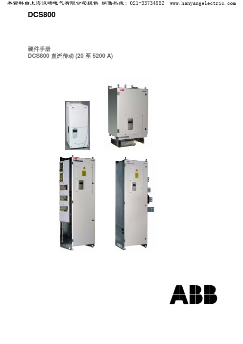
DCS800硬件手册DCS800 直流传动 (20 至5200 A)DCS800 单传动手册语言代码E D I ES F CN DCS 800 快速启动指南 (191 + CD) 3 ADT 645 0 ??DCS 800 变流器模块DCS800 彩页 3 ADW 000 190x x p p p x DCS800 控制盘方案彩页 3 ADW 000 210DCS800 技术样本 3 ADW 000 192x p p p p x DCS800 硬件手册 3 ADW 000 194x p p p p x 固件手册 3 ADW 000 193x p p p p x 符合 EMC的安装手册 3 ADW 000 032x技术指导 3 ADW 000 163xDCS800 服务手册 3 ADW 000 195p p12脉变流器的设计和启动 3 ADW 000 196pCMA-2 板 3 ADW 000 136p硬并联彩页 3 ADW 000 153p工具+ 光纤连接DriveWindow 2.x 3 BFE 645 60981xDriveOPC 3 BFE 000 73846xDDCS 通讯链选件 3 AFE 639 88235xDDCS 分配单元用户手册 3 BFE 642 85513xNETA 远程诊断接口 3 AFE 546 05062xDCS800 应用1131编程工具+库CoDeSys2.3x x1131 DCS800 目标 +工具描述3ADW000199xDCS 800XXXXX卷曲 3 ADW 000 058卷曲应用描述电磁应用彩页电磁应用描述DCS800 00A 柜体DCA 800彩页 3 ADW 000 213DCS800 00A系统描述 3 ADW 000 198p pDCS800 00A的安装 3 ADW 000 091p pDCR 500 改造组件DCR彩页 3 ADW 000 007p pDCR 手册 3 ADW 000 197pDCS500/DCS600 升级手册硬件扩展RAIO-01模拟IO 扩展3AFE 644 84567xRDIO-01 数字IO 扩展3AFE 644 85733xAIMA R-槽扩展3AFE64661442x串行通讯传动专用串行通讯安装和启动指南RPBA-12 (PROFIBUS)x现场总线适配器RPBA- (PROFIBUS) 3 AFE 645 04215x现场总线适配器 RCAN-02 (CANopen)现场总线适配器 RCNA-01 (ControlNet) 3 AFE 645 06005x现场总线适配器 RDNA- (DeviceNet) 3 AFE 645 504223x现场总线适配器RMBA (MODBUS) 3 AFE 644 98851x现场总线适配器 RETA (Ethernet)x -> 已存在 p -> 计划的DCS800 直流传动20 至5200 A硬件手册中文版:3ABD00018962基于:3ADW000194R0401 REV D:生效时间: 2006-08-28© 2006 北京ABB电气传动系统有限公司版权所有5安全须知本章内容本章包括了安装、操作和维护传动单元时必须遵守的安全须知。
小白从0学习CW32的第一天(搭建软件开发环境)

CW32IOT评估板软件例程基于MDK-arm(keil5)开发,详细安装教程请观看视频教程,或者移步至CSDN搜索KIEL5安装。
MDK注册完成后,为使WCH-LINK能正确仿真CW32,需对WCH-LINK安装驱动。
找到驱动软件包双击进行安装首先点击“DapLinkSer”文件夹安装驱动,在KEIL5环境下WCH-LINK要在“ARM”模式下,将WCH-Link切换到ARM模式,在Keil中选择CMSIS-DAP Debugger即可仿真调试.。
(9)MDK-ARM 工具链。
复制固件包“IdeSupport\MDK\flashloader”目录下的*.FLM 文件(参见图1.8)到MDK-ARM 的安装目录“Keil_v5\ARM\Flash\文件中”如图1.8图1.8图1.9(10)打开Keil MDK-ARM 微控制器集成开发环境,如图1.10:图1.10(11)在“Project”菜单中,选择“Open Project”以显示“Select Project File”对话框。
浏览并选中一个示例项目文件,点击“打开”启动它,如图1.11:图1.11(12)选择工具栏的“Option”按钮,以显示“Option”对话框,如图1.12:图1.12(13)选择“Target”项,修改“System Viewer File”为固件包“IdeSupport\MDK\”目录下的CW32F030.SFR 文件,如图1.13:图 1.13(14)选择“Debug”项,修改调试器为“CMSIS-DAP Debugger”,如图1.14:如图1.14(15)选择“Utilities”项,点击“Settings”按钮,在弹出的对话框中选择“Flash Download”项,如图1.15:图 1.15(16)点击“Add”按钮,找到“CW32F030”的Flash 烧写算法,点击“Add”按钮添加,如图1.16:图1.16(17)在“Project”菜单中选择“Rebuild all target files”以编译项目。
ChromaACSOURCE编程操作说明书
Chroma AC SOURCE 编程操作说明书——MODEL 6530一,仪器图片 (2)二,编程:产生所需的波形 (2)2.1 步进(Step)模式 (3)2.2 列表(List)模式 (5)2.3 脉冲(Pulse)模式 (7)附录模拟故障掉电编程 (9)一,仪器图片图1 仪器logo图图2 仪器整机图图3 操作面板图二,编程:产生所需的波形下面讲述三种常见的编程模式(Step、List、Pulse),可以根据所需波形而选择。
进入不同编程模式的步骤如下:<1> 开机,初始化完成后,在图4中的界面点击“MODE”键图4 进入模式选择<2>然后会显示如图5 所示界面图5 选择模式当光标聚焦在红色框中时,可以通过图3 B框中的上、下键或者滚动D来选择Step、List、Pulse模式,选择好后,按下面板中“Enter”来确认。
接下来就可以在所选模式编程了。
2.1 步进(Step)模式●此模式用于产生幅值、频率按照相同步进变化的波形,例如图6所示波形,频率不变,幅值每隔100ms降低10V(有效值)。
图6 渐变波形●●具体配置及参数说明:<1> 进入Step模式后,通过图3中A框的方向键来聚焦所需设定的参数<2>每次设定完参数后,都需要按下“Enter”键<3> V,初始电压,即输出的第一个正弦波的有效值<4> F,初始频率,输出的第一个正弦波的频率<5>一般选择Sync.source=phase phase=0,这样当启动电源时,正弦波形是从0相位输出,如果有特殊需求也可以修改相位,根修改电压的方法相同<6>dV,每步电压该变量。
通过设置此选项来设定电压每步电压的改变量,还可以设定增大(+)或者减小(-)。
类似于这种聚焦后,有下拉菜单的选项都可以通过图3 B框中的上、下键或者滚动D来选择,选择好后,按下面板中“Enter”进行确认<7>dF,每步频率该变量,跟dV的设定方法相同<8> Dwell time 是设定每步的持续时间,单位:秒(second)<9> count 用来设置步数(即步进的步数)<10> 其他参数,默认值即可图7 Step 参数配置2.2 列表(List)模式此模式可以“罗列”出几十种自己设置的波形,并且可以精确控制每种波形的时间、频率和幅值。
BLAZAR-β嵌入式教学系统使用说明及实验指示书(第1版)
Blazar β 嵌入式教学系统
4 / 57
1.1 MKL26Z256 单片机 NXP 公司的 Kinetis L 系列 MCU 将新型 ARM Cortex-M0+处理器的卓越能效 和易用性与 Kinetis 32 位 MCU 组合的性能、丰富的外设集、支持功能和可扩展 性相结合。Kinetis L 系列 MCU 还与基于 ARM Cortex-M4 的 Kinetis K 系列硬件和 软件兼容,提供了一个向更高的性能、存储器和特性集成度升级的可扩展途 径。Cortex-M0+处理器系列的超低功耗、低成本和易于使用的优点的组合,旨 在满足专门面向电动机控制、汽车、电源管理、嵌入式音频和工业自动化市场 的新兴类别的灵活解决方案。
1 概述............................................................................................................................ 4 1.1 MKL26Z256 单片机 ................................................................................................5 1.2 Blazar Beta 嵌入式教学系统组件 .........................................................................5
Dlight调试和编程Dynalite照明控制设备软件用户手册

8. 工程技术 六. 预置场景的编辑
1. 从物理视窗屏预置编辑 2. 从逻辑视窗进行预置场景的编辑 七. 打印 八. 调度管理器 1. 编译命令 2. 调度器源文件例子 九. 时钟 十. 通用传感器 十一. 可配置面板 十二. Smart 面板 十三. 手持编程器 十四. 面板模拟器 十五. 监控器 十六. 初始化文件 1. 默认的初始化文件 2. 初始化文件格式 十七. 快捷键和鼠标动作 十八. 安装(略)
图三 列表配置对话框
2. 从磁盘文件加载数据 调光器的数据文件能保存到磁盘上,能通过菜单上的<File Open> 选项加载。 DLight 在启动时能设置自动加载调光器数据文件。这是靠 Dlight.ini 文件中设置工作目录到包含有特定文件名<dx.hex>的调光器映象目 录中,d 是设备类型助记符,x 是号码。 工作目录\DYNALITE\DLIGHT\HEX\ 如果该文件(调光器映象)是 DTKD001.hex DTKD002.hex DTKD003.hex 它们都在 Directroy\DYNALITE\DLIGHT\HEX\中,于是这三个调光 器 DTK001、DTK002 和 DTK003 启动时被加载,文件名中的号用 来决定 12 通道调光器的 Box 号,4 通道调光器的 Box 号存贮在文 件 数 据 中 。( 用 DLight 选 择 Icon ( 图 像 ) 和 编 辑 它 的 特 性 (<File><Properties>)去设置工作目录。)
1. 从设备加载数据
加载存贮在调光器中的配置数据,需要在“Options”“List Config” 对话框中设置搜索信息字段(Field),这个对话框的快捷键是<L>。
TMS320F28335的C语言编程教程
Application ReportSPRAA85D–November2005–Revised January2013 Programming TMS320x28xx and28xxx Peripherals inC/C++ Lori Heustess AEC C2000ABSTRACTThis application report explores a hardware abstraction layer implementation to make C/C++coding easier on C28x devices.This method is compared to traditional#define macros and topics of code efficiency and special case registers are also addressed.Contents1Introduction (1)2Traditional#define Approach (3)3Bit Field and Register-File Structure Approach (5)4Bit Field and Register-File Structure Advantages (11)5Code Size and Performance Using Bit Fields (12)6Read-Modify-Write Considerations When Using Bit Fields (16)7A Special Case:eCAN Control Registers (21)8References (23)List of Figures1SCI SCICCR Register (9)2SCI SCICTL1Register (9)3Code Composer Studio v5.1Autocomplete Feature (12)4Code Composer Studio v5.1Expression Window (12)5Peripheral Clock Control0Register(PCLKCR0) (13)List of Tables1SCI-A,SCI-B Configuration and Control Registers (3)2SCI-A and SCI-B Common Register File (5)3CPU-Pipeline Activity For Read-Modify-Write Instructions in (14)4Read-Modify-Write Sensitive Registers (21)1IntroductionThe TMS320x28xx and TMS328x28xxx are members of the C2000™generation for embedded control applications.To facilitate writing efficient and easy-to-maintain embedded C/C++code on these devices, Texas Instruments provides a hardware abstraction layer method for accessing memory-mappedperipheral registers.This method is the bit field and register-file structure approach.This application report explains the implementation of this hardware abstraction layer and compares it to traditional#definemacros.Topics of code efficiency and special case registers are also addressed.C2000,controlSUITE,Concerto,Piccolo,Delfino,Code Composer Studio are trademarks of Texas Instruments.All other trademarks are the property of their respective owners.Introduction The hardware abstraction layer discussed in this application report has been implemented as a collection of C/C++header files available for download in controlSUITE™from Texas Instruments:Support for all new microcontrollers is available in the device support section of controlSUITE.At this time, this includes the following:•Concerto™Series Microcontrollers(C28x Subsystem)–28M35x•Piccolo™Series Microcontrollers–2806x–2802x–2803x•Delfino™Series–C2833x/C2823x–C2834x•Older C28x devices are supported in the following downloads–C281x C/C++Header Files and Peripheral Examples(SPRC097)–C280x,C2801x C/C++Header Files and Peripheral Examples(SPRC191)–C2804x C/C++Header Files and Peripheral Examples(SPRC324)Depending on your current needs,the software included in these downloads are learning tools or thebasis for a development platform.•Learning Tool:The C/C++Header Files and Peripheral Examples include several example Code Composer Studio™projects.These examples explain the steps required to initialize the device and utilize on-chipperipherals.The examples can be copied and modified to quickly experiment with peripheralconfigurations.•Development Platform:The header files can be incorporated into a project as a hardware abstraction layer for accessing on-chip peripherals using C or C++code.You can also pick and choose functions as needed and discard the rest.This application report does not provide a tutorial on C,C++,C28xx assembly,or emulation tools.You should have a basic understanding of C code and the ability to load and run code using Code Composer Studio.While knowledge of C28xx assembly is not required to understand the hardware abstraction layer, it is useful to understand the code optimization and read-modify-write sections.If you have assemblyinstruction-related questions,see the TMS320C28x CPU and Instruction Set Reference Guide(SPRU430).Examples are based on the following software versions:•C281x C/C++Header Files and Peripheral Examples(SPRC097)V1.00•C280x,C2801x C/C++Header Files and Peripheral Examples(SPRC191)V1.41•C2804x C/C++Header Files and Peripheral Examples(SPRC324)V1.00•C28x Compiler V4.1.1The following abbreviations are used:•C/C++Header Files and Peripheral Examples refers to any of the header file or device support packages.•TMS320x280x and280x refer to all devices in the TMS320x280x and TMS320x2801x family and the UCD9501.For example:TMS320F2801,TMS320F2806,TMS320F2808,TMS320F28015andTMS320F28016.•TMS320x2804x and2804x refers all devices in the TMS320x2804x family.For example,the TMS320F28044.•TMS320x281x and281x refer to all devices in the TMS320x281x family.For example:TMS320F2810, TMS320F2811,and TMS320F2812,TMS320C2810,and so forth. Traditional#define Approach •C28x refers to the TMS320C28x CPU;this CPU is used on all of the above DSPs.2Traditional#define ApproachDevelopers have traditionally used#define macros to access registers in C or C++.To illustrate thisapproach,consider the SCI-A and SCI-B register files shown in Table1.Table1.SCI-A,SCI-B Configuration and Control Registers(SPRU051).(2)These registers are reserved on devices without the SCI-B peripheral.See the data manual for details.A developer can implement#define macros for the SCI peripherals by adding definitions like those inExample1to an application header file.These macros provide an address label,or a pointer,to eachregister location.Even if a peripheral is an identical copy a macro is defined for every register.Forexample,every register in SCI-A and SCI-B is specified separately.Traditional#define Approach Example1.Traditional#define Macros/*********************************************************************Traditional header file********************************************************************/#define Uint16unsigned int#define Uint32unsigned long//Memory Map//Addr Register#define SCICCRA(volatile Uint16*)0x7050//0x7050SCI-A Communications Control#define SCICTL1A(volatile Uint16*)0x7051//0x7051SCI-A Control Register1#define SCIHBAUDA(volatile Uint16*)0x7052//0x7052SCI-A Baud Register,High Bits#define SCILBAUDA(volatile Uint16*)0x7053//0x7053SCI-A Baud Register,Low Bits#define SCICTL2A(volatile Uint16*)0x7054//0x7054SCI-A Control Register2#define SCIRXSTA(volatile Uint16*)0x7055//0x7055SCI-A Receive Status#define SCIRXEMUA(volatile Uint16*)0x7056//0x7056SCI-A Receive Emulation Data Buffer#define SCIRXBUFA(volatile Uint16*)0x7057//0x7057SCI-A Receive Data Buffer#define SCITXBUFA(volatile Uint16*)0x7059//0x7059SCI-A Transmit Data Buffer#define SCIFFTXA(volatile Uint16*)0x705A//0x705A SCI-A FIFO Transmit#define SCIFFRXA(volatile Uint16*)0x705B//0x705B SCI-A FIFO Receive#define SCIFFCTA(volatile Uint16*)0x705C//0x705C SCI-A FIFO Control#define SCIPRIA(volatile Uint16*)0x705F//0x705F SCI-A Priority Control#define SCICCRB(volatile Uint16*)0x7750//0x7750SCI-B Communications Control#define SCICTL1B(volatile Uint16*)0x7751//0x7751SCI-B Control Register1#define SCIHBAUDB(volatile Uint16*)0x7752//0x7752SCI-B Baud Register,High Bits#define SCILBAUDB(volatile Uint16*)0x7753//0x7753SCI-B Baud Register,Low Bits#define SCICTL2B(volatile Uint16*)0x7754//0x7754SCI-B Control Register2#define SCIRXSTB(volatile Uint16*)0x7755//0x7755SCI-B Receive Status#define SCIRXEMUB(volatile Uint16*)0x7756//0x7756SCI-B Receive Emulation Data Buffer#define SCIRXBUFB(volatile Uint16*)0x7757//0x7757SCI-B Receive Data Buffer#define SCITXBUFB(volatile Uint16*)0x7759//0x7759SCI-B Transmit Data Buffer#define SCIFFTXB(volatile Uint16*)0x775A//0x775A SCI-B FIFO Transmit#define SCIFFRXB(volatile Uint16*)0x775B//0x775B SCI-B FIFO Receive#define SCIFFCTB(volatile Uint16*)0x775C//0x775C SCI-B FIFO Control#define SCIPRIB(volatile Uint16*)0x775F//0x775F SCI-B Priority ControlEach macro definition can then be used as a pointer to the register's location as shown in Example2. Example2.Accessing Registers Using#define Macros/*********************************************************************Source file using#define macros********************************************************************/...*SCICTL1A=0x0003;//write entire register*SCICTL1B|=0x0001;//enable RX...Some advantages of traditional#define macros are:•Macros are simple,fast,and easy to type.•Variable names exactly match register names;variable names are easy to remember.Disadvantages to traditional#define macros include the following:•Bit fields are not easily accessible;you must generate masks to manipulate individual bits.•You cannot easily display bit fields within the Code Composer Studio watch window.•Macros do not take advantage of Code Composer Studio's auto-completion feature.•Macros do not benefit from duplicate peripheral reuse.3Bit Field and Register-File Structure ApproachInstead of accessing registers using#define macros,it is more flexible and efficient to use a bit field and register-file structure approach.•Register-File Structures:A register file is the collection of registers belonging to a peripheral.These registers are groupedtogether in C/C++as members of a structure;this is called a register-file structure.Each register-filestructure is mapped in memory directly over the peripheral registers at compile time.This mappingallows the compiler to efficiently access the registers using the CPU's data page pointer(DP).•Bit Field Definitions:Bit fields can be used to assign a name and width to each functional field within a register.Registersdefined in terms of bit fields allow the compiler to manipulate single elements within a register.Forexample,a flag can be read by referencing the bit field name corresponding to that flag.The remainder of this section describes a register-file structure with bit-field implementation for the SCI peripherals.This process consists of the following steps:1.Create a simple SCI register-file structure variable type;this implementation does not include bit fields.2.Create a variable of this new type for each of the SCI instances.3.Map the register-file structure variables to the first address of the registers using the linker.4.Add bit-field definitions for select SCI registers.5.Add union definitions to provide access to either bit fields or the entire register.6.Rewrite the register-file structure type to include the bit-field and union definitions.In the C/C++Header Files and Peripheral Examples,the register-file structures and bit fields have been implemented for all peripherals on the TMS320x28xx and TMS320x28xxx devicess.3.1Defining A Register-File StructureExample1showed a hardware abstraction implementation using#define macros.In this section,theimplementation is changed to a simple register file structure.Table2lists the registers that belong to the SCI peripheral.This register file is identical for each instance of the SCI,i.e.,SCI-A and SCI-B.Table2.SCI-A and SCI-B Common Register FileName Size Address Offset DescriptionSCICCR16bits0SCI Communications Control RegisterSCICTL116bits1SCI Control Register1SCIHBAUD16bits2SCI Baud Register,High BitsSCILBAUD16bits3SCI Baud Register,Low BitsSCICTL216bits4SCI Control Register2SCIRXST16bits5SCI Receive Status RegisterSCIRXEMU16bits6SCI Receive Emulation Data Buffer RegisterSCIRXBUF16bits7SCI Receive Data Buffer RegisterSCITXBUF16bits9SCI Transmit Data Buffer RegisterSCIFFTX16bits10SCI FIFO Transmit RegisterSCIFFRX16bits11SCI FIFO Receive RegisterSCIFFCT16bits12SCI FIFO Control RegisterSCIPRI16bits15SCI Priority Control RegisterThe code in Example3groups the SCI registers together as members of a C/C++structure.The register in the lowest memory location is listed first in the structure and the register in the highest memory location is listed last.Reserved memory locations are held with variables that are not used except as spaceholders,i.e.,rsvd1,rsvd2,rsvd3,and so forth.The register's size is indicated by its type:Uint16for16-bit (unsigned int)and Uint32for32-bit(unsigned long).The SCI peripheral registers are all16-bits so only Uint16has been used.Example3.SCI Register-File Structure Definition/*********************************************************************SCI header file*Defines a register file structure for the SCI peripheral********************************************************************/#define Uint16unsigned int#define Uint32unsigned longstruct SCI_REGS{union SCICCR_REG SCICCR;//Communications control registerunion SCICTL1_REG SCICTL1;//Control register1Uint16SCIHBAUD;//Baud rate(high)registerUint16SCILBAUD;//Baud rate(low)registerunion SCICTL2_REG SCICTL2;//Control register2union SCIRXST_REG SCIRXST;//Receive status registerUint16SCIRXEMU;//Receive emulation buffer registerunion SCIRXBUF_REG SCIRXBUF;//Receive data bufferUint16rsvd1;//reservedUint16SCITXBUF;//Transmit data bufferunion SCIFFTX_REG SCIFFTX;//FIFO transmit registerunion SCIFFRX_REG SCIFFRX;//FIFO receive registerunion SCIFFCT_REG SCIFFCT;//FIFO control registerUint16rsvd2;//reservedUint16rsvd3;//reservedunion SCIPRI_REG SCIPRI;//FIFO Priority control};The structure definition in Example3creates a new type called struct SCI_REGS.The definition alone does not create any variables.Example4shows how variables of type struct SCI_REGS are created in a way similar to built-in types such as int or unsigned int.Multiple instances of the same peripheral use the same type definition.If there are two SCI peripherals on a device,then two variables are created:SciaRegs and ScibRegs.Example4.SCI Register-File Structure Variables/*********************************************************************Source file using register-file structures*Create a variable for each of the SCI register files********************************************************************/volatile struct SCI_REGS SciaRegs;volatile struct SCI_REGS ScibRegs;The volatile keyword is very important in Example4.A variable is declared as volatile whenever its value can be changed by something outside the control of the code in which it appears.For example,peripheral registers can be changed by the hardware itself or within an interrupt.If volatile is not specified,then it is assumed the variable can only be modified by the code in which it appears and the compiler may optimize out what is seen as an unnecessary access.The compiler will not,however,optimize out any volatilevariable access;this is true even if the compiler's optimizer is enabled.3.2Using the DATA_SECTION Pragma to Map a Register-File Structure to MemoryThe compiler produces relocatable blocks of code and data.These blocks,called sections,are allocated in memory in a variety of ways to conform to different system configurations.The section to memory block assignments are defined in the linker command file.By default,the compiler assigns global and static variables like SciaRegs and ScibRegs to the .ebss or .bss section.In the case of the abstraction layer,however,the register-file variables are instead allocated to the same memory as the peripheral's register file.Each variable is assigned to a specific data section outside of .bss/ebss by using the compiler's DATA_SECTION pragma.The syntax forthe DATA_SECTION pragma in C is:#pragma DATA_SECTION (symbol ,"section name ")The syntax for the DATA_SECTION pragma in C++is:#pragma DATA_SECTION ("section name ")The DATA_SECTION pragma allocates space for the symbol in the section called section name .InExample 5,the DATA_SECTION pragma is used to assign the variable SciaRegs and ScibRegs to data sections named SciaRegsFile and ScibRegsFile .The data sections are then mapped to the same memory block occupied by the respective SCI registers.Example 5.Assigning Variables to Data SectionsThis data section assignment is repeated for each peripheral.The linker command file is then modified to map each data section directly to the memory space where the registers are mapped.For example,Table 1indicates that the SCI-A registers are memory mapped starting at address ing the assigned data section,the variable SciaRegs is allocated to a memory block starting at address 0x7050.The memory allocation is defined in the linker command file (.cmd)as shown in Example 6.For moreinformation on using the C28x linker and linker command files,see the TMS320C28x Assembly Language Tools User's Guide (SPRU513).Example6.Mapping Data Sections to Register Memory LocationsBy mapping the register-file structure variable directly to the memory address of the peripheral's registers, you can access the registers directly in C/C++code by simply modifying the required member of thestructure.Each member of a structure can be used just like a normal variable,but its name will be a bit longer.For example,to write to the SCI-A Control Register(SCICCR),access the SCICCR member of SciaRegs as shown in Example7.Here the dot is an operator in C that selects a member from astructure.Example7.Accessing a Member of the SCI Register-File Structure/*********************************************************************User's source file********************************************************************/...SciaRegs.SCICCR=SCICCRA_MASK;ScibRegs.SCICCR=SCICCRB_MASK;...3.3Adding Bit-Field DefinitionsAccessing specific bits within the register is often useful;bit-field definitions provide this flexibility.Bit fields are defined within a C/C++structure by providing a list of bit-field names,each followed by colon and the number of bits the field occupies.Bit fields are a convenient way to express many difficult operations in C or C++.Bit fields do,however, suffer from a lack of portability between hardware platforms.On the C28x devices,the following rulesapply to bit fields:•Bit field members are stored from right to left in memory.That is,the least significant bit,or bit zero,of the register corresponds to the first bit field.•The C28x compiler limits the maximum number of bits within a bit field to the size of an integer;no bit field can be greater than16bits in length.•If the total number of bits defined by bit fields within a structure grows above16bits,then the next bit field is stored consecutively in the next word of memory.The SCICCR and SCICTL1registers in Figure1and Figure2translate into the C/C++bit-field definitions in Example8.Reserved locations within the register are held with bit fields that are not used except as place holders,i.e.,rsvd,rsvd1,rsvd2,et cetera.As with other structures,each member is accessed using the dot operator in C or C++.Figure1.SCI SCICCR Register15141312111098ReservedR-07654320 STOPBITS EVEN/ODD PRIORITY LOOPBACK ADDR/IDLE SCICHARPARITY ENABLE ENA ModeR-0R/W-0R/W-0R-0R/W-0R/W-0LEGEND:R/W=Read/Write;R=Read only;-n=value after resetFigure2.SCI SCICTL1Register158ReservedR-076543210 Reserved RXERRINTENA SWRESET Reserved TXWAKE SLEEP TXENA RXENA R-0R/W-0R/W-0R-0R/W-0R/W-0R/W-0R/W-0 LEGEND:R/W=Read/Write;R=Read only;-n=value after resetExample8.SCI Control Registers Defined Using Bit Fields3.4Using UnionsWhile bit fields provide access to individual bits,you may still want to access the register as a singlevalue.To provide this option,a union declaration is created to allow the register to be accessed in terms of the defined bit fields or as a whole.The union definitions for the SCI communications control register and control register1are shown in Example9.Example9.Union Definition to Provide Access to Bit Fields and the Whole RegisterOnce bit-field and union definitions are established for specific registers,the SCI register-file structure is rewritten in terms of the union definitions as shown in Example10.Note that not all registers have bit field definitions;some registers,such as SCITXBUF,will always be accessed as a whole and a bit fielddefinition is not necessary.Example10.SCI Register-File Structure Using Unions/*********************************************************************SCI header file********************************************************************///---------------------------------------------------------------------------//SCI Register File://struct SCI_REGS{union SCICCR_REG SCICCR;//Communications control registerunion SCICTL1_REG SCICTL1;//Control register1Uint16SCIHBAUD;//Baud rate(high)registerUint16SCILBAUD;//Baud rate(low)registerunion SCICTL2_REG SCICTL2;//Control register2union SCIRXST_REG SCIRXST;//Receive status registerUint16SCIRXEMU;//Receive emulation buffer registerunion SCIRXBUF_REG SCIRXBUF;//Receive data bufferUint16rsvd1;//reservedUint16SCITXBUF;//Transmit data bufferunion SCIFFTX_REG SCIFFTX;//FIFO transmit registerunion SCIFFRX_REG SCIFFRX;//FIFO receive registerunion SCIFFCT_REG SCIFFCT;//FIFO control registerUint16rsvd2;//reservedUint16rsvd3;//reservedunion SCIPRI_REG SCIPRI;//FIFO Priority control};As with other structures,each member(.all or.bit)is accessed using the dot operator in C/C++as shown in Example11.When the.all member is specified,the entire register is accessed.When the.bit member is specified,then the defined bit fields can be directly accessed. Bit Field and Register-File Structure Advantages NOTE:Writing to a bit field has the appearance of writing to only the specified field.In reality,however,the CPU performs what is called a read-modify-write operation;the entire registeris read,its contents are modified and the entire value is written back.Possible side effects ofread-modify-write instructions are discussed in Section6.Example11.Accessing Bit Fields in C/C++/*********************************************************************User's source file********************************************************************///Access registers without a bit field definition(.all,.bit not used)SciaRegs.SCIHBAUD=0;SciaRegs.SCILBAUD=1;//Write to bit fields in SCI-A SCICTL1SciaRegs.SCICTL1.bit.SWRESET=0;SciaRegs.SCICTL1.bit.SWRESET=1;SciaRegs.SCIFFCT.bit.ABDCLR=1;SciaRegs.SCIFFCT.bit.CDC=1;//Poll(i.e.,read)a bitwhile(SciaRegs.SCIFFCT.bit.CDC==1){}//Write to the whole SCI-B SCICTL1/2registers(use.all)ScibRegs.SCICTL1.all=0x0003;ScibRegs.SCICTL2.all=0x0000;4Bit Field and Register-File Structure AdvantagesThe bit field and register-file structure approach has many advantages that include:•Register-file structures and bit fields are already available from Texas Instruments.In the C/C++Header Files and Peripheral Examples,the register-file structures and bit fields havebeen implemented for all peripherals on the TMS320x28xx and TMS320x28xxx devices.The includedheader files can be used as-is or extended to suit your particular needs.The complete implementation is available in the software downloads from TI's website as shown inSection1.•Using bit fields produces code that is easy-to-write,easy-to-read,easy-to-update,and efficient.Bit fields can be manipulated quickly without the need to determine a register mask value.In addition,you have the flexibility to access registers either by bit field or as a single quantity as shown inExample11.Code written using the register file structures also generates very efficient code.Codeefficiency will be discussed in Section5.•Bit fields take advantage of the Code Composer Studio editors auto complete feature.At first it may seem that variable names are harder to remember and longer to type when usingregister-file structures and bit fields.The Code Composer Studio editor provides a list of possiblestructure/bit field elements as you type;this makes it easier to write code without referring todocumentation for register and bit field names.An example of the auto completion feature for the CPU-Timer TCR register is shown in Figure3.11 SPRAA85D–November2005–Revised January2013Programming TMS320x28xx and28xxx Peripherals in C/C++Code Size and Performance Using Bit Fields Figure3.Code Composer Studio v5.1Autocomplete Feature•Increases the effectiveness of the Code Composer Studio Watch Window.You can add and expand register-file structures in Code Composer Studio's watch window as shown in Figure4.Bit field values are read directly without extracting their value by hand.Figure4.Code Composer Studio v5.1Expression Window5Code Size and Performance Using Bit FieldsThe bit field and register-file structure approach is very efficient when accessing a single bit within aregister or when polling a bit.As an example,consider code to initialize the PCLKCR0register on aTMS320x280x device.PCLKCR0is described in detail in the TMS320x280x,2801x,2804x SystemControl and Interrupts Reference Guide(SPRU712).The bit-field definition for this register is shown in Example12.12Programming TMS320x28xx and28xxx Peripherals in C/C++SPRAA85D–November2005–Revised January2013 Code Size and Performance Using Bit FieldsFigure5.Peripheral Clock Control0Register(PCLKCR0)15141312111098 ECANBENCLK ECANAENCLK Reserved SCIBENCLK SCIAENCLK SPIBENCLK SPIAENCLK R/W-0R/W-0R-0R/W-0R/W-0R/W-0R/W-0 76543210 SPIDENCLK SPICENCLK Reserved I2CAENCLK ADCENCLK TBCLKSYNC Reserved R/W-0R/W-0R-0R/W-0R/W-0R/W-0R-0LEGEND:R/W=Read/Write;R=Read only;-n=value after resetExample12.TMS320x280x PCLKCR0Bit-Field Definition//Peripheral clock control register0bit definitions:struct PCLKCR0_BITS{//bits descriptionUint16rsvd1:2;//1:0reservedUint16TBCLKSYNC:1;//2eWPM Module TBCLK enable/syncUint16ADCENCLK:1;//3Enable high speed clk to ADCUint16I2CAENCLK:1;//4Enable SYSCLKOUT to I2C-AUint16rsvd2:1;//5reservedUint16SPICENCLK:1;//6Enable low speed clk to SPI-CUint16SPIDENCLK:1;//7Enable low speed clk to SPI-DUint16SPIAENCLK:1;//8Enable low speed clk to SPI-AUint16SPIBENCLK:1;//9Enable low speed clk to SPI-BUint16SCIAENCLK:1;//10Enable low speed clk to SCI-AUint16SCIBENCLK:1;//11Enable low speed clk to SCI-BUint16rsvd3:2;//13:12reservedUint16ECANAENCLK:1;//14Enable SYSCLKOUT to eCAN-AUint16ECANBENCLK:1;//15Enable SYSCLKOUT to eCAN-B};The code in Example13enables the peripheral clocks on a TMS320x2801device.The C28x compiler generates one assembly code instruction for each C-code register access.This is very efficient;there is a one-to-one correlation between the C instructions and the assembly instructions.The only overhead is the initial instruction to set the data page pointer(DP).Example13.Assembly Code Generated by Bit Field AccessesC-Source Code Generated AssemblyMemory Instruction//Enable only2801Peripheral ClocksEALLOW;3F82A7EALLOW3F82A8MOVW DP,#0x01C0SysCtrlRegs.PCLKCR0.bit.rsvd1=0;3F82AA AND@28,#0xFFFCSysCtrlRegs.PCLKCR0.bit.TBCLKSYNC=0;3F82AC AND@28,#0xFFFBSysCtrlRegs.PCLKCR0.bit.ADCENCLK=1;3F82AE OR@28,#0x0008SysCtrlRegs.PCLKCR0.bit.I2CAENCLK=1;3F82B0OR@28,#0x0010SysCtrlRegs.PCLKCR0.bit.rsvd2=0;3F82B2AND@28,#0xFFDFSysCtrlRegs.PCLKCR0.bit.SPICENCLK=1;3F82B4OR@28,#0x0040SysCtrlRegs.PCLKCR0.bit.SPIDENCLK=1;3F82B6OR@28,#0x0080SysCtrlRegs.PCLKCR0.bit.SPIAENCLK=1;3F82B8OR@28,#0x0100SysCtrlRegs.PCLKCR0.bit.SPIBENCLK=1;3F82BA OR@28,#0x0200SysCtrlRegs.PCLKCR0.bit.SCIAENCLK=1;3F82BC OR@28,#0x0400SysCtrlRegs.PCLKCR0.bit.SCIBENCLK=0;3F82BE AND@28,#0xF7FFSysCtrlRegs.PCLKCR0.bit.rsvd3=0;3F82C0AND@28,#0xCFFFSysCtrlRegs.PCLKCR0.bit.ECANAENCLK=1;3F82C2OR@28,#0x4000SysCtrlRegs.PCLKCR0.bit.ECANBENCLK=0;3F82C4AND@28,#0x7FFFEDIS;3F82C6EDIS13 SPRAA85D–November2005–Revised January2013Programming TMS320x28xx and28xxx Peripherals in C/C++。
VISTA-120主机编程指南(简)及一些简单操作命令
1. VISTA-120防区编程指南(简)输入:41408000 进入编程出现:PROGRAM MODE*Fill # View-00输入:*97(恢复出厂值)出现:LOOD DEFAULTS0=NO 1=YES输入: 1出现:SYSTEM DEFAULTS(稍后几秒,数据既消除)出现:PROGRAM MODE*FILE* VIEW----00输入:*93 (进入模块编程)出现:ZONE PROGRAM?1=YES 0=NO输入:1出现:SET TO CONFIRM1=YES 0=NO输入: 1出现:ENTER ZONE NO。
000=QUIT 001输入:011 *(例如对011号防区编程)出现:011ZT P RC IN:L00-- -- -- --:--输入:*出现:011 ZONE RESPONSENO RESPONSE 00输入:07(24小时有声防区)/03(周边窃警防区)/01(延时防区)出现:011 ZONE RESPONSE24HR AUDILLE 07输入:*出现:011 PARTITION 1输入:*(输入相应的子系统号码)(注:不分子系统的话默认都属于第1个子系统)出现:011 REPORT CODE1ST 00 2ND 00 00输入:*(输入相应的防区报告码)输入:*输入:*出现:011 INPUT TYPE(选择探头类型)NONE 00输入:06(总线制)(注:对于接在总线上的模块都需要输入06)出现:011 INPUT TYPESERIAL POLL 06输入:*出现:011 SMART CONTACT1=YES 0=NO 0输入:*出现:011V-PLEX RELAY1=YES 0=NO 0 (注:如果是带继电器的模块则要输入1)输入:*出现:011D00R #(01—15) 00输入:*出现:011 INPUT S/N:LA xxxx---xxxx 0输入:A095-1566 1(4293SN模块上的码)(注:只有编4193SN模块时后面的1需要改为2)输入:*出现:Xmit To confirmPress * to skip输入:*出现: ZT P RC INL03 1 30 SL1s输入: *出现: ENTER ZONE NO000=QUIT 012(注:下一个防区设置,如要退出则输入000)输入: 000输入:*问是否要退出0=NO 1=YES输入:1出现:PROGRAM MODEFILL*VIEW 00输入:*99退出2. 4101SN 模块编程与注意事项进行继电器编程(注:使用4101SN模块时要剪掉里面的白色电阻,另外自带防区电阻10K)在防区编程把继电器的地址码编好后,就要对继电器进行事件启动、停止与继电器的对应输出的编程。
上海维宏电子科技股份有限公司 NcStudio-V15 激光平面切割控制系统 厂商手册说明书
NcStudio-V15 激光平面切割控制系统厂商手册(LS1500、LS3000、LS8000M)版次:2023 年04 月04 日第2.2 版作者:激光加工产品部上海维宏电子科技股份有限公司版权所有目录1快速入门 (1)1.1概述 (1)1.2硬件连接示意图 (2)1.3快捷键一览 (4)2机床安装 (5)2.1概述 (5)2.2安装随动仪放大器 (5)2.3安装运动控制卡 (6)2.4安装软件 (7)2.5安装驱动程序 (8)2.5.1自动安装驱动程序 (8)2.5.2手动安装驱动程序 (9)3系统调试 (12)3.1概述 (12)3.2设置 NcConfig (13)3.2.1备份数据 (13)3.2.2恢复数据 (14)3.2.3配置设备并映射端口 (15)3.2.4保护端口 (17)3.4设置驱动器参数 (19)3.4.1设置非总线驱动器参数 (19)3.4.2设置总线驱动器参数 (50)3.5设置总线系统参数 (54)3.6设置速度参数 (55)3.7设置脉冲当量 (55)3.8调整轴方向 (58)3.9设置工作台行程 (58)3.10使用丝杠误差补偿 (59)3.10.1使用反向间隙补偿 (59)3.10.2使用双向补偿 (59)3.11检测机床设置 (61)3.11.1检测脉冲当量和电子齿轮比 (61)3.11.2检测脉冲 (61)3.11.3检测激光工艺 (62)3.12进行机床老化 (63)3.13安装和使用摄像头 (64)3.13.1修改计算机 IP 地址 (65)3.13.2修改摄像头 IP 地址 (66)4随动调试 (68)4.1概述 (68)4.1.1页面切换区 (69)4.1.2随动控制区/随动参数设置区 (69)4.1.3坐标显示区 (73)4.1.4手动控制区 (73)4.1.5随动控制按钮 (74)4.2操作 (75)4.2.1执行准备项 (75)4.2.2检测电容 (75)4.2.4执行标定 (76)4.2.5检查随动仪放大器 (78)4.3参数 (79)4.3.1系统设置参数 (79)4.3.2跟随设置参数 (81)4.3.3随动仪参数 (82)4.3.4标定设置参数 (84)4.3.5速度设置参数 (86)4.3.6实时状态检测参数 (87)4.3.7Z手动速度 (87)4.4常见问题 (88)4.4.1电气干扰严重 (88)4.4.2碰板电容不为零 (89)4.4.3标定时切割头碰板仍继续向下运动 (89)4.4.4设置跟随高度与实际跟随高度有偏差 (90)4.4.5电容反馈正常,标定结果良好,切割头频繁停止工作 (90)4.4.6切薄板时切割头抖动严重,导致切割工件轮廓发生变形 (90)4.4.7点动Z轴或直接开随动时系统报警‚随动错误状态‛ (91)4.4.8编码器方向或轴方向出错 (91)4.4.9随动到位等待超时 (92)4.4.10跟随误差偏大 (92)4.4.11系统空闲或加工过程中开跟随碰板报警 (93)4.4.12系统静态下碰板报警 (94)4.4.13跟随过冲 (94)5电气接线图 (95)5.1端子板 (95)5.1.1Lambda 控制器 (95)5.1.2扩展端子板 (98)5.2激光器 (101)5.2.1IPG-YLR 系列激光器 (102)5.2.2飞博 MARS-500W 激光器 (102)5.2.3锐科 Raycus 光纤激光器 (103)5.2.4JK / GSI-500W-FL 激光器 (104)5.2.5创鑫Max光纤激光器 (105)5.2.6SPI-500W-R4 激光器 (106)5.2.7海富HFB 1000-1500W 激光器 (107)5.2.8GW SMATLas 3S 激光器 (108)5.3驱动器接线图 (109)5.3.1驱动器接口定义 (109)5.3.2驱动器接线图(位置环控制模式) (111)5.3.3驱动器接线图(速度环控制模式) (134)6手柄简介 (151)6.1WHB05L(V4) 无线手柄 (152)6.2WHB05L(V5) 无线手柄 (154)6.3WHB05N(V1) 无线手柄 (156)6.4产品规格参数 (158)6.5使用注意事项 (158)6.6常见问题 (159)法律声明 (160)1快速入门1.1概述NcStudio V15 激光切割控制系统由硬件和软件组成:∙硬件o PM95A 运动控制卡o Lambda 控制器:▪非总线控制系统:Lambda 5E 控制器▪总线控制系统:Lambda NE 控制器o EX33A 扩展端子板(控制随动)o EX31A 扩展端子板(扩展端子接口)o SE001 随动仪放大器o DB9M/F 通讯线 2 根o射频电缆线 1 根o M16 三芯航空插头拖链电缆线1根o WHB05L 无线手柄 / WHB05N 无线手柄各个硬件之间的连接示意图参见硬件连接示意图。
DIXELL操作手册
dIXELL目录1. 注意事项1. 注意事项_______________________________22. 用户界面_______________________________33. 远程面板 VICX610_______________________54. 面板的显示信息________________________5 ∙ 此手册作为产品的一部分应放在控制器附近,以便快速查阅。
5. 蜂鸣器静音_____________________________66. 首次安装使用___________________________6 ∙此控制器不得作以下说明以外的其他用途,不得作安全保护设备使用。
7. RTC 内置时钟的设置____________________6 8. 如何使用“HOT KEY ”热键编程钥匙________6 ∙控制器投入运行前检查应用量程。
9. 使用面板上的键盘进行参数编程_________710. 更改密码_______________________________7 11. 启动/停止制冷或热泵工作模式___________8 12. 待机功能_______________________________8 ∙ 进行连接前确认电源电压是否正确。
13. “menu” 功能菜单_________________________8 ∙不要让温控器在有水或潮湿的环境中使用:温控器只能在使用环境限定的条件下使用,应避免在高湿度环境下温度的剧烈变化而使得水蒸气凝结在内部的电路板上。
14. 键盘功能_______________________________9 15. 远程开关机_____________________________9 16. 在线关闭压缩机_______________________10 ∙ 注意:在检修前请断开温控器电源,最好断开所有连接线路,以防止意外发生。
CCS3.3, SEED XDS510, 2812安装及使用
CCS3.3, SEED XDS510, 2812安装及使用一、CCS3.3的安装安装软件CCS3.3,双击安装文件:点击下一步,点确定,点击Finish完成安装。
二、安装驱动程序以SEED XDS510为例,如果是HELLO DSP或者其他类型仿真器,请参照其他说明文档。
点击安装文件安装完成后,插入仿真器会提示找到硬件:安装硬件完成后,设备管理器显示如下:三、配置CCS3.3点击程序菜单中的Setup Code Composer Studio v3.3,进入如下界面:按如下步骤进行配置:配置项注意选择seedxds510plus.cfg,其他均为默认值。
配置完成后保存设置。
四、CCS3.3使用主控板插上SEED仿真器,注意对齐,方向不要连错,仿真器插错可能会导致仿真器烧坏。
电脑连接仿真器USB线,打开CCS3.3软件,选择连接,如下图所示:连接成功后,主界面左下角会显示连接成功图标。
点击如下图所示小图标,进入烧写程序界面。
点击左下方的Flash Programmer Settings…按钮,选择FlashAPIInterface2812V2_10.out文件在On-Chip Flash Programme对话框中的Operation栏下,设置为自己编译生成的待烧入Flash的.out文件的路径,如下图所示:选择相应的烧写文件后,点击On-Chip Flash Programme对话框中的Execute Operation按钮,即可执行程序的烧写,如下图所示:如提示File not found,选择No不必理会。
烧写完毕后,可以按F5运行程序观察运行效果。
烧写操作完成后,断电,拔掉仿真器插头,重新上电,程序即可正常运行。
- 1、下载文档前请自行甄别文档内容的完整性,平台不提供额外的编辑、内容补充、找答案等附加服务。
- 2、"仅部分预览"的文档,不可在线预览部分如存在完整性等问题,可反馈申请退款(可完整预览的文档不适用该条件!)。
- 3、如文档侵犯您的权益,请联系客服反馈,我们会尽快为您处理(人工客服工作时间:9:00-18:30)。
技术员专用编程书
一.基本命令:
“5555”默认安装员密码,“1234”默认管理员密码
#退出或从新输入
*用来命令具体操作
*0快速布撤防
*1旁路(撤防状态),激活防区(布防状态);
*2显示故障状态;
*3报警记录;
*4门铃功能开/关(键盘声音)也可通过门铃快捷键来实现;
*5用户密码编辑(操作具体功能需加管理员密码);
*6用户命令(操作具体功能需加管理员密码);
*7X命令功能1-4(命令或控制PGM输出);
*8安装员编程(操作具体功能需加安装员密码);
*9无进入延时布防(操作具体功能需加管理员密码);
辅助功能键:(PK键盘右侧详见键盘图案)长按2秒;
1在家布防
2外出布防
3门铃功能打开/关闭
4火警探测器复位
5快速退出
二.具体编程:
A.用户密码编辑:(可直接输入新的3位密码编号进行下一个密码编程)
a.编程:*5+管理员密码+密码序号(01-39)+XXXXXX(四位或六位);
b.更改:*5+管理员密码+密码序号(01-39)+新XXXXXX(四位或六位);
c.删除:*5+管理员密码+密码序号(01-39)+*
B.用户密码属性定义:
*5+管理员密码+密码序号(01-39)+99+密码属性定义(详见编程手册)
C.日期编程:
*6+管理员密码+功能1(时间/日期编程,其余选项详见编程手册)+HH:MM MM/DD/YY
三.进入编程:
*8+安装员密码(默认55555)
四.防区定义(详见说明书P28):
进入编程+001(子系统选择001-004)+防区号(01-16)+防区定义(01进入延时1,02进入延时2,
03即时防区,16为24小时防区,详见编程说明书);
五.系统时间(详见说明书P29):(进入延时有效030-255,退出延时045-255)
进入编程+005+01(01-04子系统序号)+时间XXX(进入延时1+进入延时2+键盘退出延时)+09+响铃时间xxx(001-255)
六.键盘注册(详见说明书P28):定义键盘控制的相应子系统
进入编程+000+0(进入键盘分配)+X(子系统号,1-8,0是全局键盘)+X(键盘地
址1-8);
七.键盘锁定与解除(详见说明书P30):001-255为有效数字,000为无效;
进入编程+012+000(允许出错密码次数)+000(无操作锁定时间);
八.系统选项(详见说明书P31):子系统的系统选项;
进入编程+013
九.键盘防区规划(详见说明书P32):定义键盘控制相应的防区
进入编程+020+XX(键盘地址01-64)
十.防区属性编程(详见P34-P35):
进入编程+编程项(101-164)+防区号+防区类型
十一.电话的编程:
进入编程+350通讯格式(详见P43),165最大拔号次数(详见P36),166等待握手音时间(详见P36),167等待通讯确认时间(详见P37),301第一电话号码,302第二电话号码,303第三电话号码。
十二.报告码传输选项(详见P43-P44);
十三.其他报警报告码(详见P42):
进入编程+345(连续输入16个‘0’,关闭所有向手机拔号的故障)
进入编程+346连续输入16个‘0’。
注:
退出查看报警记忆:布防撤防一下就可以了
旁路:在撤防状态下按*1+需要旁路的防区
修改密码:007+新密码(最多6位数字,修改密码后,若出现四声短响,说明操作正常修改成功,若二声长响说明操作错误修改失败)
十四.PC1832连接法
1为四芯总线(RED BLK YEL GRN)是传输数据的,主要可对应着键盘PK5501或者PK1555键盘
的红黑黄绿连接。
2为防区接入线(Z1COM Z2......),Z1和COM对应一个防区;Z2和COM又对应一个防区接,以此类推。
3为报警喇叭接入线(BELL+-),接一个12V的声光警号,若出现异常可在警号两端并接一个1K 电阻。
4为提供一个+12V直流电压输出的接口。
5为可编程输出口:(PGM1~PGM2)通过编程可以实现它不同的输出方式,如可以编程为高低电平输出时可以接继电器进行控制
6为电话线接口,报警主机报警时候可以拨通电话进行报告事件。
注:
将电话连接端子(TIP,Ring,T-1,R-1)的线路连接到RJ31电话接口。
请使用26AWG以上的线缆;要将多个设备连入电话线请按顺序连接,电话格式在编程项[350];
报警中心号码在编程项[351]-[376]
7为接地端口:(EGND)
8为备用蓄电池接入口,当交流电掉电时候就起备用电源的作用提供给主机工作。
9为交流电输入,交流电源变压器建议为16.5V40VA。
PK5501键盘
Z端口和B两个可以接一个门磁,或者你也可以不用。
TL150的接法
红黑黄绿接主机,RJ45接到网络到路由器。
需要和网络软件一起配合使用。