BSS84中文资料
全中文芯片资料TSS721A仪表总线收发器
仪表总线收发器
1、概述
TSS721A 是满足仪表总线标准(EN1434-3)的单芯片收发器,内部接口电路可以适应仪表总线 结构中主从机之间的不同电平,与总线的连接是无极性的,且支持使用光耦与从机间进行全电隔离。 芯片可由总线供电,对从机不增加功率需求,并内置总线电压故障指示。接收器有动态电平识别功 能,发送器有可编程电流沉。片内集成 3.3v 稳压源,当总线发生故障时将会延时关断。该电路广泛 应用于 M-BUS 远程抄表、安防、智能家居等领域。
第 4 页,共 9 页
650 μA
350 μA
0.5 μA
0.5 μA
3.4
V
5
Ω
6.4
4.3
V
7.5
2.4 mA
1.1
1.33 V
VSTC
V
1
MΩ
VBAT
0.6
V
0.9
3
s
QQ:37056373 V.1.0
TSS721A 仪表总线收发集成电路
注 2:输入端 RX/RXI 及输出端 TX/TXI 端悬空,ICC=ICI1+ICI2。 3.4 接收模块直流参数
2.2 引脚说明
引脚 1 2 3 4 5 6 7 8 9 10 11 12 13 14 15 16
符号 BUSL2
VB STC RIDD PF SC TXI TX BAT VS VDD RX RXI RIS GND BUSL1
功能描述 连接仪表总线 整流后总线信号端 外接电源维持电容 外接 CS1 电流值调节电阻 欠压指示输出端 外接采样电容 数据信号反相输出端 数据信号输出端 逻辑电平调整输入端 总线/电池供电模式切换输出端 稳压电源输出端 数据信号输入端 数据信号反相输入端 外接调制电流值调节电阻
BZX84C16LT1G中文资料
BZX84B4V7LT1,BZX84C2V4LT1 Series Zener Voltage Regulators225 mW SOT−23 Surface MountThis series of Zener diodes is offered in the convenient, surface mount plastic SOT−23 package. These devices are designed to provide voltage regulation with minimum space requirement. They are well suited for applications such as cellular phones, hand held portables,and high density PC boards.Features•Pb−Free Packages are Available•225 mW Rating on FR−4 or FR−5 Board•Zener Breakdown V oltage Range − 2.4 V to 75 V•Package Designed for Optimal Automated Board Assembly •Small Package Size for High Density Applications•ESD Rating of Class 3 (>16 KV) per Human Body Model •Tight Tolerance Series Available (See Page 4)Mechanical CharacteristicsCASE: V oid-free, transfer-molded, thermosetting plastic case FINISH: Corrosion resistant finish, easily SolderableMAXIMUM CASE TEMPERATURE FOR SOLDERING PURPOSES:260°C for 10 SecondsPOLARITY: Cathode indicated by polarity band FLAMMABILITY RATING: UL 94 V−0MAXIMUM RATINGSMaximum ratings are those values beyond which device damage can occur.Maximum ratings applied to the device are individual stress limit values (not normal operating conditions) and are not valid simultaneously. If these limits are exceeded, device functional operation is not implied, damage may occur and reliability may be affected.1.FR−5 = 1.0 X 0.75 X 0.62 in.2.Alumina = 0.4 X 0.3 X 0.024 in., 99.5% alumina.See specific marking information in the device marking column of the Electrical Characteristics table on page 3 of this data sheet.DEVICE MARKING INFORMATION(Pinout: 1-Anode, 2-No Connection, 3-Cathode)(T A = 25°Cunless otherwise noted, V F = 0.95 V Max. @ I F = 10 mA)ELECTRICAL CHARACTERISTICS − BZX84CxxxLT1 SERIES (STANDARD TOLERANCE) (Pinout: 1-Anode, 2-No Connection, 3-Cathode)(T A = 25°C unless otherwise noted, V F = 0.90 V Max. @ I F = 10 mA) (Devices listed in bold, italic are ON Semiconductor Preferred devices.)Z*The “G” suffix indicates Pb−Free package available.ELECTRICAL CHARACTERISTICS − BZX84BxxxL (Tight Tolerance Series)(Pinout: 1-Anode, 2-No Connection, 3-Cathode)(T A = 25°C unless otherwise noted, V F = 0.90 V Max. @ I F = 10 mA)Z*The “G” suffix indicates Pb−Free package available.V Z , T E M P E R A T U R E C O E F F I C I E N T (m V /C )°θV Z , NOMINAL ZENER VOLTAGE (V)− 3− 2012345678Figure 1. Temperature Coefficients (Temperature Range −55°C to +150°C)V Z , T E M P E R A T U R E C O E F F I C I E N T (m V /C )°θ100101V Z , NOMINAL ZENER VOLTAGE (V)Figure 2. Temperature Coefficients (Temperature Range −55°C to +150°C)V Z , NOMINAL ZENER VOLTAGEFigure 3. Effect of Zener Voltage onZener ImpedanceZ Z T , D Y N A M I C I M P E D A N C E ()Ω1000100101V F , FORWARD VOLTAGE (V)Figure 4. Typical Forward VoltageI F , F O R W A R D C U R R E N T (m A )1000100101C , C A P A C I T A N C E (p F )V Z , NOMINAL ZENER VOLTAGE (V)Figure 5. Typical Capacitance 1000100101V Z , ZENER VOLTAGE (V)1001010.10.01I Z , Z E N ER C U R R E N T (m A )V Z , ZENER VOLTAGE (V)1001010.10.01I R , L E A K A G E C U R R E N T (A )µV Z , NOMINAL ZENER VOLTAGE (V)Figure 6. Typical Leakage Current10001001010.10.010.0010.00010.00001I Z , Z E N E R C U R R E N T (m A )Figure 7. Zener Voltage versus Zener Current(V Z Up to 12 V)Figure 8. Zener Voltage versus Zener Current(12 V to 91 V)PACKAGE DIMENSIONSSOT−23TO−236AB CASE 318−09ISSUE AK*For additional information on our Pb−Free strategy and solderingdetails, please download the ON Semiconductor Soldering and Mounting Techniques Reference Manual, SOLDERRM/D.SOLDERING FOOTPRINT*ǒmm inchesǓSCALE 10:1ON Semiconductor and are registered trademarks of Semiconductor Components Industries, LLC (SCILLC). SCILLC reserves the right to make changes without further notice to any products herein. SCILLC makes no warranty, representation or guarantee regarding the suitability of its products for any particular purpose, nor does SCILLC assume any liability arising out of the application or use of any product or circuit, and specifically disclaims any and all liability, including without limitation special, consequential or incidental damages.“Typical” parameters which may be provided in SCILLC data sheets and/or specifications can and do vary in different applications and actual performance may vary over time. All operating parameters, including “Typicals” must be validated for each customer application by customer’s technical experts. SCILLC does not convey any license under its patent rights nor the rights of others. SCILLC products are not designed, intended, or authorized for use as components in systems intended for surgical implant into the body, or other applications intended to support or sustain life, or for any other application in which the failure of the SCILLC product could create a situation where personal injury or death may occur. Should Buyer purchase or use SCILLC products for any such unintended or unauthorized application, Buyer shall indemnify and hold SCILLC and its officers, employees, subsidiaries, affiliates, and distributors harmless against all claims, costs, damages, and expenses, and reasonable attorney fees arising out of, directly or indirectly, any claim of personal injury or death associated with such unintended or unauthorized use, even if such claim alleges that SCILLC was negligent regarding the design or manufacture of the part. SCILLC is an Equal Opportunity/Affirmative Action Employer. This literature is subject to all applicable copyright laws and is not for resale in any manner.PUBLICATION ORDERING INFORMATION。
ELM842B中文资料(ELM Technology)中文数据手册「EasyDatasheet - 矽搜」
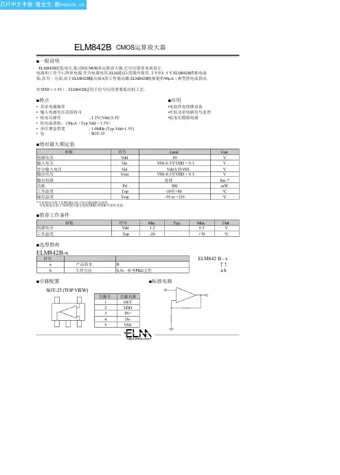
ELM842B CMOS运算放大器
■电气特性(VDD = 1.5V)
参数 输入偏移电压 输入偏置电流 共模输入电压范围 最大输出电压摆幅 最大输出源电流 开环增益 共模抑制比 电源电压抑制比 目前消费 单位增益带宽 压摆率
符号
条件
Vio
Vout=Vdd/2
Hale Waihona Puke IibVcmrVouts Vid=100mV, RL=200kΩ
1 nA
0.04
2.90 V
2.80
V
45 100
μA
80
dB
85
dB
80
dB
145 280 μA
1
MHz
0.45 1.00
V/μs
■标识
SOT-25
No.
Mark
a
C
b
0 to 9
c
0 to 9
内容
ELM842B
批号 批号
芯片中文手册,看全文,戳
ELM842B CMOS运算放大器
ELM842B CMOS运算放大器
■典型特征
源电流 - Vdd
200 180 160 140 120 100
电流8(0 A)
60 40 20
0 123456
Vdd (V) 源电流 - 热门
200
150
100
电流(A)
50
Vdd=3V Vdd=1.5V
-20 -10 0
200 180 160 140 120 100
■Note
1)负载电阻 ELM842B是专为低功耗应用;因此,输出源电流仅为90μA(典型值在VDD = 1.5V).其结果是, ELM842B不能试图驾驶小负载电阻时,以防护持输出电压摆幅.考虑到这一点,负载和反馈电阻为 ELM842B应仔细选择.
BZX84C4V3V中文资料
SILIICON PLANAR VOLTAGE REGULATOR DIODEBZX84C2V4 to 75V SOT-23Formed SMD PackageLow voltage general purpose voltage regulator diode ABSOLUTE MAXIMUM RATINGS (T a =25°C)UNIT %Repetitive Peak Forward Current mA Repetitive Peak Working Current mA mW mW °C °CTHERMAL RESISTANCE K/W* Device mounted on a ceramic alumna** Device mounted on an FR5 printed circuit boardELECTRICAL CHARACTERISTICS (T a =25°C unless specified otherwise) Device Temperature DifferentialI R at V RMarkingCoefficient ResistanceS Z (mV/K)rdiff (Ω)µAat I Z test=5mA at I Z test=1mAmin max min max max Max (V)BZX84C2V4 2.20 2.60 -3.560050 1.0Z11BZX84C2V72.50 2.90 -3.560020 1.0Z12BZX84C3V0 2.80 3.20 -3.560010 1.0Z13BZX84C3V3 3.10 3.50 -3.5600 5.0 1.0Z14BZX84C3V6 3.40 3.80 -3.5600 5.0 1.0Z15BZX84C3V9 3.70 4.10-3.56003.0 1.0Z16BZX84C4V34.00 4.60 -3.5600 3.0 1.0Z17BZX84C4V7 4.40 5.00 -3.5 0.2500 3.0 2.0Z1BZX84C5V1 4.80 5.40 -2.7 1.2480 2.0 2.0Z2BZX84C5V6 5.20 6.00 -2.0 2.5400 1.0 2.0Z3BZX84C6V2 5.80 6.60 0.4 3.7150 3.0 4.0Z4BZX84C6V8 6.407.20 1.2 4.580 2.0 4.0Z5BZX84C7V57.007.90 2.5 5.380 1.0 5.0Z6BZX84C8V27.708.70 3.2 6.2800.7 5.0Z7BZX84C9V18.509.60 3.8 7.01000.5 6.0Z8BZX84C109.4010.604.5 8.01500.27.0Z9BZX84C2V4_75V Rev_060506E*** Pulse Test 20ms < tp < 50ms1515152060401015909090801001009595 + 5VALUE max I ZRM Storage Temperature T stg Junction to Ambient*R th (j-a)DESCRIPTIONI FRM Working Voltage Tolerance Power Dissipation upto T a =25ºC SYMBOL *P D ***V Z ( + 5%)(V)at I Z test=5mA Resistance rdiff (Ω)at I Z test=5mA250420300- 65 to +150250Forward Voltage at V F <0.9V at 10mA and <1.5V at 200mAVoltage 150250Differential Working Power Dissipation upto T c =25ºC **P D Junction Temperature T j Pin Configuration1 = A N ODE2 = N C3 =CATHODE12Continental Device India LimitedAn ISO/TS 16949, ISO 9001 and ISO 14001 Certified CompanySILIICON PLANAR VOLTAGE REGULATOR DIODEBZX84C2V4 to 75V SOT-23Formed SMD PackageELECTRICAL CHARACTERISTICS (T a =25°C unless specified otherwise) Device Temperature DifferentialI R at V RMarkingCoefficientResistanceS Z (mV/K)rdiff (Ω)µAat I Z test=5mAat I Z test=1mA min max min max max Max (V)BZX84C1110.4011.60 5.4 9.01500.18Y1BZX84C1211.4012.70 6.0 101500.18Y2BZX84C1312.4014.10 7.0 111700.18Y3BZX84C1513.8015.60 9.2 132000.0510.5Y4BZX84C1615.3017.10 10.4 142000.0511.2Y5BZX84C1816.8019.10 12.4 162250.0512.6Y6BZX84C2018.8021.20 14.4 182250.0514.0Y7BZX84C2220.8023.30 16.4 202500.0515.4Y8BZX84C2422.8025.60 18.4 222500.0516.8Y9at I Z Test=2mA at I Z Test=0.5mABZX84C2725.1028.90 21.4 25.33000.0518.9Y10BZX84C3028.0032.00 24.4 29.43000.0521.0Y11BZX84C3331.0035.00 27.4 33.43250.0523.1Y12BZX84C3634.0038.00 30.4 37.43500.0525.2Y13BZX84C3937.0041.00 33.4 41.23500.0527.3Y14BZX84C4340.0046.00 37.6 46.63750.0530.1Y15BZX84C4744.0050.00 42.0 51.83750.0532.9Y16BZX84C5148.0054.00 46.6 57.24000.0535.7Y17BZX84C5652.0060.00 52.2 63.84250.0539.2Y18BZX84C6258.0066.00 58.8 71.64500.0543.4Y19BZX84C6864.0072.00 65.6 79.84750.0547.6Y20BZX84C7570.0079.0073.4 88.65000.0552.5Y21BZX84C2V4_75V Rev_060506E*** Pulse Test 20ms < tp < 50ms2002152402551301501701808080908025303070at I Z test=5mA at I Z test=5mA max at I Z test=2mAat I Z Test=2mA4045555520Resistance ***V Z ( + 5%)rdiff (Ω)(V)Forward Voltage at V F <0.9V at 10mA and <1.5V at 200mAWorking Differential Voltage Pin Configuration1 = A N ODE2 = N C3 =CATHODE12BZX84C2V4 to 75V SOT-23Formed SMD PackageSOT-23 Package Reel InformationReel specification for W" Packing (13" reel)BZX84C2V4_75V Rev_060506ESOT-23 Formed SMD PackageTape Specification for SOT-23 Surface Mount DeviceS O T -23 T &R3K /reel 10K /reel136 g m /3K p c s 415 g m /10K p c s3" x 7.5" x 7.5"9" x 9" x 9"13" x 13" x 0.5"12 K 51 K 10 K17" x 15" x 13.5"19" x 19" x 19"17" x 15" x 13.5"192 K 408 K 300 K12 k g s 28 k g s 16 k g sPACKAGEN e t W e i g h t /Q t y DetailsS T A N D A R D PACKI N N E R C A R T O N B O XQ t y O U T E R C A R T O N B O XQ t y G r W t SizeSizePacking Detail±0.0114.47.9 – 10.9T R A I L E RF I X I N GT A P EL E A D E R9.2±0.5MAXNOTES:No. of Devices8mm Tape Size of Reel 330 mm (13")10,000 Pcs 8mm Tape Size of Reel 180 mm (7")3,000 Pcs1.The bandolier of 330 mm reel contains at least 10,000 devices.2.The bandolier of 180 mm reel contains at least 3,000 devices.3.No more than 0.5% missing devices / reel. 50 empty compartments for 330 mm reel.15 empty compartments for 180 mm reel.4.Three consecutive empty places might be found provided this gap is followed by 6 consecutive devices.5.The carrier tape (leader) starts with at least 75 empty positions (equivalent to 330 mm).In order to fix the carrier tape a self adhesive tape of 20 to 50 mm is applied. At the end of the bandolier at least 40 empty positions (equivalent to 160 mm) are there.3.15Customer Notes BZX84C2V4 to 75VSOT-23Formed SMD Package1. CDIL Semiconductor Devices are RoHS compliant, customers are requested to pleasedispose as per prevailing Environmental Legislation of their Country.2. In Europe, please dispose as per EU Directive 2002/96/EC on Waste Electrical andElectronic Equipment (WEEE).BZX84C2V4_75V Rev_060506E DisclaimerThe product information and the selection guides facilitate selection of the CDIL's Semiconductor Device(s)best suited for application in your product(s)as per your requirement.It is recommended that you completely review our Data Sheet(s)so as to confirm that the Device(s)meet functionality parameters for your application.The information furnished in the Data Sheet and on the CDIL Web Site/CD are believed to be accurate and reliable.CDIL however,does not assume responsibility for inaccuracies or incomplete information.Furthermore,CDIL does not assume liability whatsoever,arising out of the application or use of any CDIL product;neither does it convey any license under its patent rights nor rights of others. These products are not designed for use in life saving/support appliances or systems.CDIL customers selling these products(either as individual Semiconductor Devices or incorporated in their end products),in any life saving/support appliances or systems or applications do so at their own risk and CDIL will not be responsible for any damages resulting from such sale(s).CDIL strives for continuous improvement and reserves the right to change the specifications of its products without prior notice.CDIL is a registered Trademark ofContinental Device India LimitedC-120 Naraina Industrial Area, New Delhi 110 028, India.Telephone + 91-11-2579 6150, 4141 1112 Fax + 91-11-2579 5290, 4141 1119email@ 。
BZX84C9V1S-7-F中文资料
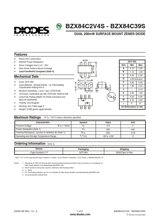
Lead-freeBZX84C2V4S - BZX84C39SDUAL 200mW SURFACE MOUNT ZENER DIODEFeaturesMaximum Ratings@ T A = 25°C unless otherwise specified* Add “-7-F” to the appropriate type number in Table 1 from Sheet 2 example: 6.2V Zener = BZX84C6V2S-7-F.Notes: 1. Mounted on FR4 PC Board with recommended pad layout which can be found on our website at /datasheets/ap02001.pdf.2. Short duration test pulse used to minimize self-heating effect.3. f = 1KHz.4. For Packaging Details, got to our website at /datasheets/ap02007.pdf.5. No purposefully added lead.(Note 4)Ordering InformationElectrical Characteristics@ T A = 25°C unless otherwise specifiedNotes: 6. Short duration test pulse used to minimize self-heating effect. 7. f = 1KHz.Date Code KeyKXX = Product Type Marking Code YM = Date Code Marking Y = Year ex: N = 2002M = Month ex: 9 = SeptemberKXX YMK X X Y M Marking Information102030405012345678910I , Z E N E R C U R R E N T (m A )Z V , ZENER VOLTAGE (V)Z Fig. 2 Zener Breakdown CharacteristicsC , T O T A L C A P A C I T A N C E (p F )T 101001000V , NOMINAL ZENER VOLTAGE (V)Z Fig. 4. Total Capacitance vs Nominal Zener VoltageT , AMBIENT TEMPERATURE, (°C)A Fig. 1. Power Derating CurveP , P O W E R D I S S I P A T I O N (m W )D 200100300001002000102030I , Z E N E R C U R R E N T (m A )Z V , ZENER VOLTAGE (V)Z Fig. 3, Zener Breakdown Characteristics10203040IMPORTANT NOTICEDiodes Incorporated and its subsidiaries reserve the right to make modifications, enhancements, improvements, corrections or other changes without further notice to any product herein. Diodes Incorporated does not assume any liability arising out of the application or use of any product described herein; neither does it convey any license under its patent rights, nor the rights of others. The user of products in such applications shall assume all risks of such use and will agree to hold Diodes Incorporated and all the companies whose products are represented on our website, harmless against all damages.LIFE SUPPORTDiodes Incorporated products are not authorized for use as critical components in life support devices or systems without the expressed written approval of the President of Diodes Incorporated.。
AD7847资料

8/13 ±3 2.4 0.8 ±1 8
8/13 ±3 2.4 0.8 ±1 8
8/13 ±3 2.4 0.8 ±1 8
kΩ min/max % max
V min V max µA max pF max Ω typ mA typ
Digital Inputs at 0 V and VDD
0.2 15
0.2 15
DD SS REFA REFB L L OUT FB MIN MAX
Parameter STATIC PERFORMANCE Resolution Relative Accuracy2 Differential Nonlinearity2 Zero Code Offset Error2 @ +25°C TMIN to TMAX Gain Error2 @ +25°C TMIN to TMAX REFERENCE INPUTS VREF Input Resistance VREFA, VREFB Resistance Matching DIGITAL INPUTS Input High Voltage, VINH Input Low Voltage, VINL Input Current Input Capacitance3 ANALOG OUTPUTS DC Output Impedance Short Circuit Current POWER REQUIREMENTS VDD Range VSS Range Power Supply Rejection ∆Gain/∆VDD ∆Gain/∆VSS IDD ISS
V min/max V min/max % per % max % per % max mA max mA max µs typ V/µs typ nV secs typ VDD = 15 V ± 5%, VREF = –10 V VSS = –15 V ± 5%, VREF = +10 V Output Unloaded. Typically 5 mA Output Unloaded. Typically 4 mA Settling Time to Within ± 1/2 LSB of Final Value. DAC Latch Alternately Loaded with All 0s and All 1s DAC Latch Alternately Loaded with 01 . . . 11 and 10 . . . 00 VREFA = 20 V p-p, 10 kHz Sine Wave. DAC Latches Loaded with All 0s VREFB = 20 V p-p, 10 kHz Sine Wave. DAC Latches Loaded with All 0s VREF = 20 V p-p, 10 kHz Sine Wave. DAC Latch Loaded with All 0s V REF = 100 mV p-p Sine Wave. DAC Latch Loaded with All 1s VREF = 20 V p-p Sine Wave. DAC Latch Loaded with All 1s VREF = 6 V rms, 1 kHz. DAC Latch Loaded with All 1s Code Transition from All 0s to All 1s See Typical Performance Graphs Amplifier Noise and Johnson Noise of RFB
BSS64;中文规格书,Datasheet资料
50
100
1
10 100 I C - COLLECTOR CURRE NT (mA)
200
/
BSS64
NPN General Purpose Amplifier
(continued)
Typical Characteristics
1 0.8
β = 10
V BEON - BASE EMITTER ON VOLTAGE (V)
SMALL SIGNAL CHARACTERISTICS
fT Cob Current Gain - Bandwidth Product Output Capacitance IC = 4.0 mA, VCE = 10, f = 35 MHz VCB = 10 V, f = 1.0 MHz 60 5.0 MHz pF
Absolute Maximum Ratings*
Symbol
VCEO VCBO VEBO IC TJ, Tstg Collector-Emitter Voltage Collector-Base Voltage Emitter-Base Voltage Collector Current - Continuous
TA = 25°C unless otherwise noted
Parameter
Value
80 120 5.0 200 -55 to +150
Units
V V V mA °C
Operating and Storage Junction Temperature Range
*These ratings are limiting values above which the serviceability of any semiconductor device may be impaired.
cs8411cs8412中文资料pdf数字音频接口接收机芯片
的差动电压,信号幅度必须超过 400mVp-p。这就意味着这个幅度最小值是 CP340/1201 和
IEC-958(这两种信号接口和 RS-422 不适配)所指定的最小 200mVp-p 的两倍。
开关特性-CS8411 并口(TA=25ºC 对于后缀“-CP”和“-CS”,TA=-40 到 85ºC 对于
Iin
±10
mA
输入电压,除 RXP、RXN 以外的任何角
VIN
-0.3
VD++0.3
V
输入电压,RXP 和 RXN
VIN
-12
12
V
工作环境温度(提供电源)
TA
-55
125
ºC
存储温度
Tstg
-65
150
ºC
注 1:电流瞬间达到 100mA 不会引起 SCR 打开。
注意:在这些限制条件之外工作可能会导致器件永久的损坏。正常工作不允许在这些最大最
3
电子发烧友 电子技术论坛
存储器,通过一个并口读数据,这个存储器可以缓存通道状态、用户数据和可选的辅助数据。 CS8412 把通道状态、用户数据和有效信息直接分离出来送给串行输出角,它为最重要的通 道状态比特位提供输出角。这 2 个芯片还包含内容广泛的出错报告以及用于自动设置的对接 收到的音频信号采样频率的指示。
CS8412 把通道、用户和有效数据直接分离到串行输出口的输出角上,串行输出口为最 重要的通道状态位提供输出角。
定购信息参看原文 32 页
性能/特性
绝对最大工作额定值(GND=0V,所有电压都对地测量得到)
参量
符号
最小值
最大值
单位
电源压
VD+,VA+
S-AU84中文资料
TOSHIBA RF Power Amplifier ModuleS-AU84Power Amplifier Module for Japan cdmaOneFeatures· High output power: Po = 27.5 dBmW (min)· Low operating current : I CC = 415 mA (typ.) @Po = 27.5 dBmW V CC = 3.5 V 1X modulation : I CC = 140 mA (typ.)@Po = 17.0 dBmW V CC = 1.3 V1X modulation · Low idle current : I CC (idle) = 52 mA (typ.) @V CC = 3.5 V, VDC = 3.6 V,Vcon = 2.8 V· Low leakage current : I CC (leak) = 10 µA (max)@V CC = 3.5 V, VDC = 3.6 V, Vcon = 0 V · Low-voltage operation : Operation at V CC = 1.3 V is possible.@Po = 17.0 dBmW· Compact package: 6.0 mm × 6.0 mm × 1.55 mm (5-6B package)Maximum Ratings (Ta = 25°C)Characteristics Symbol RatingUnitSupply voltage 1 V CC1 6 V Supply voltage 2 V CC2 6 V Bias circuit voltage VDC 6V Control voltage Vcon4VCollector current I CC 1 A Power dissipationP D (Note) 2WOperating temperature T op -20 to +85 °C Storage temperature rangeT stg-40 to +125 °CNote: Ta = 25°CMarking and Pin AssignmentWeight: 0.12 g (typ.)(1) Pin(2) V CC1 (3) V CC2 (4) GND (5) GND (6) GND(7) Pout (8) V DC (9) Vcon (10) GND (11) GND (12) GND(4)(5)(6)(9)(8)(7)Characteristics Symbol Test Condition Min Typ. Max UnitCollector idle current I CC (idle) ¾52 75 mABias circuit current IDC (idle) ¾ 0.5 2.0 mA Control current Icon (idle) V CC1 = V CC2 = 3.5 V, VDC = 3.6 V, Vcon = 2.8 V Pi = no input¾ 2.5 4.0 mA I CC (leak) ¾ ¾ 10 m A Leakage currentIDC (leak) V CC1 = V CC2 = 3.5 V, VDC = 3.6 V,Vcon = 0 V Pi = no input¾¾ 10 m AOutput power 1 Po1 V CC1 = V CC2 = 3.5 V, VDC = 3.6 V, Vcon = 2.8 V Pi = adjust27.5 28.0 ¾ dBmW Power gain 1 Gp1 25.027.5¾ dBCollector current 1 I CC1 ¾ 415 440mABias circuit current 1 IDC1 ¾ 2.5 4.0 mA Control current 1 Icon1 ¾ 3.5 5.0 mA Input VSWR 1VSWRin1 ¾ 2.0 3.5 ¾ Receiving band noise 1 NRB1 ¾ -139 -137dBmW/Hz 2nd harmonics 1 2fo1 ¾ -35 -30dBc 3rd harmonics 1 3fo1 V CC1 = V CC2 = 3.5 V, VDC = 3.6 V, Vcon = 2.8 V Po = 27.5 dBmW¾ -45 -40dBc Out-of-band noise 1N-3MHz1 fo = 888 MHz¾ -45 -40dBmW Adjacent-channel leakage powerratio 1ACPR1 D f = ±900 kHz (Note 2)¾ -49 -46dBc Adjacent-channel leakage power ratio 2ACPR2 D f = ±1.98 MHz (Note 2)¾ -59 -56dBc Adjacent-channel leakage power ratio 3ACPR3 D f = ±900 kHz (Note 2)¾ -50 -46dBc Adjacent-channel leakage power ratio 4ACPR4D f = ±1.98 MHz (Note 2)V CC1 = V CC2 = 3.3 V,VDC = 3.3 V,Vcon = 2.8 VPo = 26.5 dBmW¾-62-58dBcStability 1 SPR1V CC1 = V CC2 = 1.0 V to 4.2 V, VDC = 3.6 V, Vcon = 2.8 V, Po = 27.5 dBmW, ZG = 50 W , Load VSWR = 5:1 all phase, Ta = -20°C to 85°C¾ ¾ -55dBcLoad mismatch 1 ¾ V CC1 = V CC2 = 3.5 V, VDC = 3.6 V, Vcon = 2.8 V, Po = 0-27.5 dBmW, Pi = adjust, ZG = 50 W , VSWR LOAD 7:1 all phase No degradation ¾Power gain 2 Gp2 22.0 25.5 28.0dB Collector current 2 I CC2 ¾ 140 160mABias circuit current 2 IDC2 ¾ 0.8 2.5 mA Control current 2Icon2 V CC1 = V CC2 = 1.3 V, VDC = 3.6 V, Vcon = 2.8 V, Po = 17.0 dBmW¾ 2.5 4.0 mAAdjacent-channel leakage power ratio 5ACPR5 D f = ±900 kHz (Note 2)¾ -50 -46dBc Adjacent-channel leakage power ratio 6ACPR6D f = ±1.98 MHz (Note 2)¾-64-58dBcCaution: The RF power amplifier is sensitive to electrostatic discharge. When handling this product, ensure that theenvironment is protected against electrostatic discharge by using an earth strap, a conductive mat and an ionizer.Characteristics Symbol Test Condition Min Typ. Max UnitOutput power 2 Po2 V CC1 = V CC2 = 3.5 V, VDC = 3.6 V,Vcon = 2.8 V Pi = adjust27.5 28.0 ¾ dBmW Power gain 3 Gp3 25.027.5¾ dBCollector current 3 I CC3 ¾ 435 460mABias circuit current 3 IDC3 ¾ 2.5 4.0 mA Control current 3 Icon3 ¾ 3.5 5.0 mA Input VSWR 2VSWRin2 ¾ 2.0 3.5 ¾ Receiving band noise 2 NRB2 ¾ -138 -136dBmW/Hz 2nd harmonics 2 2fo2 ¾ -35 -30dBc 3rd harmonics 2 3fo2 V CC1 = V CC2 = 3.5 V, VDC = 3.6 V, Vcon = 2.8 V Po = 27.5 dBmW¾-45 -40dBc Out-of-band noise 2N-3MHz2 fo = 888 MHz¾ -44 -40dBmW Adjacent-channel leakage power ratio 7ACPR7 D f = ±900 kHz (Note 2)¾ -55 -50dBc Adjacent-channel leakage power ratio 8ACPR8 D f = ±1.98 MHz (Note 2)¾ -58 -55dBc Adjacent-channel leakage power ratio 9ACPR9 D f = ±900 kHz (Note 2)¾ -50 -46dBc Adjacent-channel leakage power ratio 10ACPR10D f = ±1.98 MHz (Note 2)V CC1 = V CC2 = 3.3 V,VDC = 3.3 V,Vcon = 2.8 VPo = 26.5 dBmW¾-60-56dBcStability 2 SPR2V CC1 = V CC2 = 1.0 V to 4.2 V, VDC = 3.6 V, Vcon = 2.8 V, Po = 27.5 dBmW, ZG = 50 W , Load VSWR = 5:1 all phase, Ta = -20°C to 85°C¾ ¾ -55dBcLoad mismatch 2 ¾ V CC1 = V CC2 = 3.5 V, VDC = 3.6 V, Vcon = 2.8 V, Po = 0-27.5 dBmW, Pi = adjust, ZG = 50 W , VSWR LOAD 7:1 all phase No degradation ¾Power gain 4 Gp4 22.0 25.0 28.0dB Collector current 4 I CC4 ¾ 145 165mABias circuit current 4 IDC4 ¾ 0.8 2.5 mA Control current 4Icon4 V CC1 = V CC2 = 1.3 V, VDC = 3.6 V, Vcon = 2.8 V, Po = 17.0 dBmW¾ 2.5 4.0 mAAdjacent-channel leakage power ratio 11ACPR11 D f = ±900 kHz (Note 2)¾ -50 -46dBc Adjacent-channel leakage power ratio 12ACPR12D f = ±1.98 MHz (Note 2)¾-64-58dBcNote1: I CC = Current of a V CC1 terminal + current of a V CC2 terminalNote2: ACPRa) Pc (1.23 MHz) is average power measured for 1.23 MHz bandwidth with carrier frequency. b) P (30 kHz) is average power measured for 30 kHz bandwidth with 900 kHz/1.98 MHz offset. c) ACPR1 (or ACPR2) = P (30 kHz) - P c (1.23 MHz) dB Note3: These electrical characteristics are measured using Toshiba standard test board in Toshiba standardmeasurement system.Electrical Characteristics 3(1X modulation, f = 887-925 MHz, Tc =-20~85°C, Zg = Zl = 50 W)Characteristics Symbol TestCondition MinTyp.Max UnitPower gain 5 Gp5 V CC1= V CC2= 3.5 V, VDC = 3.6 V,Vcon = 2.8 V, Po = 27.5 dBmW23.5 ¾¾ dBAdjacent-channel power ratio 13 ACPR13 D f =±900 kHz(Note 2)¾¾-45dBcAdjacent-channel power ratio 14 ACPR14D f =±1.98 MHz(Note 2)¾¾-54dBcElectrical Characteristics 4(IS-95 modulation, f = 887-925 MHz, Tc =-20~85°C, Zg = Zl = 50 W)Characteristics Symbol TestCondition MinTyp.Max UnitPower gain 6 Gp6 V CC1= V CC2= 3.5 V, VDC = 3.6 V,Vcon = 2.8 V, Po = 27.5 dBmW23.5 ¾¾ dBAdjacent-channel power ratio 15 ACPR15 D f =±900 kHz(Note 2)¾¾-48dBcAdjacent-channel power ratio 16 ACPR16D f =±1.98 MHz(Note 2)¾¾-54dBcPackage DimensionsWeight: 0.12 g (typ.) 1 . 5 5±0 . 1 5· TOSHIBA is continually working to improve the quality and reliability of its products. Nevertheless, semiconductor devices in general can malfunction or fail due to their inherent electrical sensitivity and vulnerability to physical stress. It is the responsibility of the buyer, when utilizing TOSHIBA products, to comply with the standards of safety in making a safe design for the entire system, and to avoid situations in which a malfunction or failure of such TOSHIBA products could cause loss of human life, bodily injury or damage to property.In developing your designs, please ensure that TOSHIBA products are used within specified operating ranges as set forth in the most recent TOSHIBA products specifications. Also, please keep in mind the precautions and conditions set forth in the “Handling Guide for Semiconductor Devices,” or “TOSHIBA Semiconductor Reliability Handbook” etc.. · The TOSHIBA products listed in this document are intended for usage in general electronics applications (computer, personal equipment, office equipment, measuring equipment, industrial robotics, domestic appliances, etc.). These TOSHIBA products are neither intended nor warranted for usage in equipment that requires extraordinarily high quality and/or reliability or a malfunction or failure of which may cause loss of human life or bodily injury (“Unintended Usage”). Unintended Usage include atomic energy control instruments, airplane or spaceship instruments, transportation instruments, traffic signal instruments, combustion control instruments, medical instruments, all types of safety devices, etc.. Unintended Usage of TOSHIBA products listed in this document shall be made at the customer’s own risk. · Gallium arsenide (GaAs) is a substance used in the products described in this document. The dust or vapor is harmful to the body. Do not break , cut, crush or dissolve chemically. · The information contained herein is presented only as a guide for the applications of our products. No responsibility is assumed by TOSHIBA CORPORATION for any infringements of intellectual property or other rights of the third parties which may result from its use. No license is granted by implication or otherwise under any intellectual property or other rights of TOSHIBA CORPORATION or others. · The information contained herein is subject to change without notice.020704EACRESTRICTIONS ON PRODUCT USE。
BSS145中文资料
Ordering Code Q67000-S132
RDS(on) 3.5 Ω
Package SOT-23
Tape and Reel Information E6327
Marking SBs
Maximum Ratings Parameter Drain source voltage Drain-gate voltage RGS = 20 kΩ Gate source voltage Gate-source peak voltage,aperiodic Continuous drain current TA = 31 °C DC drain current, pulsed TA = 25 °C Power dissipation TA = 25 °C
Parameter
Symbol
Values
min.
typ.
max.
Dynamic Characteristics Transconductance VDS≥ 2 * ID * RDS(on)max, ID = 0.2 A Input capacitance VGS = 0 V, VDS = 25 V, f = 1 MHz Output capacitance VGS = 0 V, VDS = 25 V, f = 1 MHz Reverse transfer capacitance VGS = 0 V, VDS = 25 V, f = 1 MHz Turn-on delay time VDD = 30 V, VGS = 10 V, ID = 0.2 A RGS = 50 Ω Rise time VDD = 30 V, VGS = 10 V, ID = 0.2 A RGS = 50 Ω Turn-off delay time VDD = 30 V, VGS = 10 V, ID = 0.2 A RGS = 50 Ω Fall time VDD = 30 V, VGS = 10 V, ID = 0.2 A RGS = 50 Ω
- 1、下载文档前请自行甄别文档内容的完整性,平台不提供额外的编辑、内容补充、找答案等附加服务。
- 2、"仅部分预览"的文档,不可在线预览部分如存在完整性等问题,可反馈申请退款(可完整预览的文档不适用该条件!)。
- 3、如文档侵犯您的权益,请联系客服反馈,我们会尽快为您处理(人工客服工作时间:9:00-18:30)。
handbook, halfpage
−600
MLD196
handbook, halfpage
60
MLD198
ID (mA) −400
RDSon (Ω) 40
VGS = −2.5 V −3 V −4 V −5 V
−200
20 −7.5 V −10 V
0 0
−2
−4
−6
−8 −10 VGS (V)
0 −1
LIMITING VALUES In accordance with the Absolute Maximum Rating System (IEC 134). SYMBOL VDS VGSO ID IDM Ptot Tstg Tj PARAMETER drain-source voltage (DC) gate-source voltage (DC) drain current (DC) peak drain current total power dissipation storage temperature operating junction temperature Tamb ≤ 25 °C; note 1 open drain CONDITIONS − − − − − −65 − MIN. MAX. −50 ±20 −130 −520 250 +150 150
Marking code: SP g
handbook, halfpage
BSS84
PINNING - SOT23 PIN 1 2 3 SYMBOL g s d DESCRIPTION gate source drain
3 d
s 1 Top view 2
MAM188
Fig.1 Simplified outline and symbol.
1997 Jun 18
4
元器件交易网
Philips Semiconductors
Product specification
P-channel enhancement mode vertical D-MOS transistor
BSS84
handbook, halfpage
1.2
handbook, halfpage
(1)
1.8
MLD194
k
k
(2)
1.0
1.4
0.8
1.0
0.6 −50
0
50
100
Tj (°C)
150
0.6
−50
0
50
100
Tj (°C)
150
V GSth at T j k = ------------------------------------V GSth at 25 ° C ID = −1 mA; VDS = VGS.
Pδ=tp T NhomakorabeaDC
100 ms
tp
0 0 50 100 150 200 Tamb (°C)
t T
−1
−1
−10
VDS (V)
−102
δ = 0.01. Tamb = 25 °C. (1) RDSon limitation.
Fig.4 Power derating curve.
Fig.5 DC SOAR.
R DSon at T j k = ---------------------------------------R DSon at 25 ° C (1) ID = −130 mA; VGS = −10 V. (2) ID = −20 mA; VGS = −2.4 V.
Fig.10 Temperature coefficient of gate-source threshold voltage.
Fig.3 Input and output waveforms.
handbook, halfpage
300
MLD199
−103 handbook, halfpage ID (mA) −102 (1)
MLD251
Ptot (mW)
tp = 10 µs 100 µs 1 ms
200
10 ms
100
−10
VGS = 0; Tj = 25 °C; f = 1 MHz. Tj = 25 °C.
Fig.6
Capacitance as a function of drain source voltage; typical values.
Fig.7 Typical output characteristics.
80
MLD191
handbook, halfpage
−600 ID
MLD197
C (pF) 60
VGS = −10 V −7.5 V
−6 V
(mA) −400 −5 V
40 Ciss 20 Coss
−200
−4 V
−3 V
Crss 0 0 −10 −20 VDS (V) −30
−2.5 V 0 0 −2 −4 −6 −8 −10 −12 VDS (V)
元器件交易网
Philips Semiconductors
Product specification
P-channel enhancement mode vertical D-MOS transistor
FEATURES • Low threshold voltage • Direct interface to C-MOS, TTL, etc. • High-speed switching • No secondary breakdown. APPLICATIONS • Line current interrupter in telephone sets • Relay, high speed and line transformer drivers. DESCRIPTION P-channel enhancement mode vertical D-MOS transistor in a SOT23 SMD package. CAUTION The device is supplied in an antistatic package. The gate-source input must be protected against static discharge during transport or handling. QUICK REFERENCE DATA SYMBOL VDS VGSO VGSth ID RDSon Ptot PARAMETER drain-source voltage (DC) gate-source voltage (DC) gate-source threshold voltage drain current (DC) drain-source on-state resistance total power dissipation ID = −130 mA; VGS = −10 V Tamb ≤ 25 °C open drain ID = −1 mA; VDS = VGS CONDITIONS − − −0.8 − − − MIN.
−10
−102
ID (mA)
−103
Tj = 25 °C. VDS = −10 V; Tj = 25 °C.
Fig.9 Fig.8 Typical transfer characteristics.
Drain-source on-state resistance as a function of drain current; typical values.
BSS84
UNIT V V mA mA mW °C °C
THERMAL CHARACTERISTICS SYMBOL Rth j-a PARAMETER thermal resistance from junction to ambient CONDITIONS note 1 VALUE 500 UNIT K/W
MAX. −50 ±20 −2 −130 10 250
UNIT V V V mA Ω mW
1997 Jun 18
2
元器件交易网
Philips Semiconductors
Product specification
P-channel enhancement mode vertical D-MOS transistor
BSS84
handbook, halfpage
VDD = −40 V
handbook, halfpage
10 %
INPUT 90 %
10 %
0V −10 V ID 50 Ω
MLD189
OUTPUT 90 % ton toff
MBB690
Fig.2 Switching time test circuit.
Note to the Limiting values and Thermal characteristics 1. Device mounted on a printed-circuit board. CHARACTERISTICS Tj = 25 °C unless otherwise specified. SYMBOL V(BR)DSS VGSth IDSS PARAMETER drain-source breakdown voltage gate-source threshold voltage drain-source leakage current CONDITIONS VGS = 0; ID = −10 µA VDS = VGS ; ID = −1 mA VGS = 0; VDS = −40 V VGS = 0; VDS = −50 V VGS = 0; VDS = −50 V; Tj = 125 °C IGSS RDSon yfs Ciss Coss Crss ton toff gate leakage current drain-source on-state resistance forward transfer admittance input capacitance output capacitance reverse transfer capacitance VDS = 0; VGS = ±20 V VGS = −10 V; ID = −130 mA VDS = −25 V; ID = −130 mA VGS = 0; VDS = −25 V; f = 1 MHz VGS = 0; VDS = −25 V; f = 1 MHz VGS = 0; VDS = −25 V; f = 1 MHz VGS = 0 to −10 V; VDD = −40 V; ID = −200 mA VGS = −10 to 0 V; VDD = −40 V; ID = −200 mA MIN. −50 −0.8 − − − − − 50 − − − − − TYP. − − − − − − − − 25 15 3.5 MAX. − −2 −100 −10 −60 ±10 10 − 45 25 12 − − UNIT V V nA µA µA nA Ω mS pF pF pF