Optimisation of sample thickness for THz-TDS measurements
炭_炭复合材料抗氧化涂层厚度的光学金相测量
廖寄乔等 : 炭 / 炭复合材料抗氧化涂层厚度的光学测量
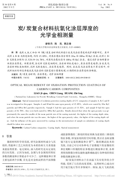
( a)
试样 A 的涂层结构图
( b)
试样 B 的涂层结构图
( c)
试样 C 的涂层 结构图 图3
( d) 经图像处理后的抗氧化涂层图像
试样 D 的涂层 结构图
表 1 试样的涂层厚度
编号 A B C D 孔隙度 ( %) 15. 85 15. 85 13. 52 16. 78 B4 C 粒度 / m 1 10 10 10 涂层平 均厚度 / m 240. 11 216. 42 208. 96 270. 83 厚度最 大值 / m 486. 11 268. 34 278. 00 386. 78 厚度最 小值 / m 67. 68 21. 26 85. 21 90. 34 ( a) 孔隙度为 15. 85% B4 C 粒度 1 m ( b) 孔隙度为 15. 85% B4 C 粒度 10 m
w as investigated in this paper . Samples A and B had the same open porosity of 15. 85% , which were coated by 1 m B4 C particles and 10 m B4 C part icles r espectiv ely. Sample C had the open porosity of 13. 52% , and sample D had the open porosit y of 16. 78% , they w er e bot h coated by 10 m B4 C particles. Results showed that when the open po rosity w as ap proximately the same the smaller of the mean particle size of t he coating material, the hig her of the coating depth value, and w hen the mean particle size was the same, the higher of the open porosity value, t he hig her of t he coating depth v al ue. A nd the influence of the pores uncovered by coatings in the microstructure of sample o n calculation of coating depth should be taken into account.
优美斯(Optimax Systems)的相位平移干扰光学测量方法白皮书说明书

The Effect Of Phase Distortion On InterferometricMeasurements Of Thin Film Coated Optical SurfacesJon Watson, Daniel SavageOptimax Systems, 6367 Dean Parkway, Ontario, NY USA*********************©Copyright Optimax Systems, Inc. 2010This paper discusses difficulty in accurately interpreting surface form data from a phase shifting interferometer measurement of a thin film interference coated surfaces.PHASE-SHIFTING INTERFEROMETRYPhase-shifting interferometry is a metrology tool widely used in optical manufacturing to determine form errors of an optical surface. The surface under test generates a reflected wavefront that interferes with the reference wavefront produced by the interferometer 1. A phase-shifting interferometer modulates phase by slightly moving the reference wavefront with respect to the reflected test wavefront 2 . The phase information collected is converted into the height data which comprises the surface under test3.Visibility of fringes in an interferometer is a function of intensity mismatch between the test and reference beams. Most commercially available interferometers are designed to optimize fringe contrast based on a 4% reflected beam intensity. If the surface under test is coated for minimum reflection near or at the test wavelength of the interferometer, the visibility of the fringe pattern can be too low to accurately measure.OPTICAL THIN-FILM INTERFERENCE COATINGSOptical thin-film interference coatings are structures composed of one or more thin layers (typically multiples of a quarter-wave optical thickness) of materials deposited on the surface of an optical substrate.The goal of interference coatings is to create a multilayer film structure where interference effects within the structure achieve a desired percent intensity transmission or reflection over a given wavelength range.The purpose of the coating defines the design of the multilayer structure. Basic design variables include:• Number of layers• Thickness of each layer• Material of each layerThe most common types of multilayer films are high reflector (HR) and anti-reflection (AR) coatings. HR coatings function by constructively interfering reflected light, while AR coatings function by destructively interfering reflected light. These coatings are designed to operate over a specific wavelength range distributed around a particular design wavelength.To produce the desired interference effects, thin-film structures are designed to modulate the phase of the reflected or transmitted wavefront. The nature of the interference effect depends precisely on the thickness of each layer in the coating as well as the refractive index of each layer. If the thickness and index of each layer is uniform across the coated surface, the reflected wavefront will have a constant phase offset across the surface. However, if layer thicknesses or index vary across the coated surface, then the phase of thereflected wavefront will also vary. Depending on the design of the coating and the severity of the thickness or index non-uniformity, the distortion of the phase of the reflected wavefront can be severe. 4Layer thickness non-uniformity is inherent in the coating process and is exaggerated by increasing radius of curvature of the coated surface.5 All industry-standard directed source deposition processes (thermal evaporation, sputtering, etc) result in some degree of layer thickness non-uniformity.5 Even processes developed to minimize layer non-uniformity, such as those used at Optimax, will still result in slight layer non-uniformity (within design tolerance).TESTING COATED OPTICS INTERFEROMETRICALLYPhase-shifting interferometers use phase information to determine the height map of the surface under test. However, surfaces coated with a thin-film interference coating can have severe phase distortion in the reflected wavefront due to slight layer thickness non-uniformities and refractive index inhomogeneity. Therefore, the measured irregularity of a coated surface measured on a phase shifting interferometer at a wavelength other than the design wavelength, may not represent the actual irregularity of the surface. Even using a phase shifting interferometer at the coating design wavelength does not guarantee accurate surface irregularity measurements. If a coating has very low reflectance over any given wavelength range (such as in the case of an AR coating), the phase shift on reflection with wavelength will vary significantly in that range.7 Figure 1 shows an example of how the phase can vary with coating thickness variations.Figure 1In this particular case, if a point at the lens edge has the nominal coating thickness and the coating at lens center is 2% thicker, expect ~38° phase difference in the measurement (~0.1 waves). This will erroneous be seen as height by the interferometer, despite the actual height change in this case being less than 7nm (~0.01 waves). Also, depending on coating design, low fringe visibility may inhibit measurements.There is an extreme method to determine the irregularity of a thin-film interference coated surface by flash coating it with a bare metal mirror coating. A metal mirror coating is not a thin-film interference coating, and the surface of the mirror represents the true surface, This relatively expensive process requires extra time, handling, and potential damage during the metal coating chemical strip process.CONCLUSIONS•There can be practical limitations to getting accurate surface form data on coated optical surfaces due to issues with phase distortion and fringe visibility.•The issues are a function of thin film coating design particulars and the actual deposition processes.1 R.E. Fischer, B. Tadic-Galeb, P. Yoder, Optical System Design, Pg 340, McGraw Hill, New York City, 20082 H.H. Karow, Fabrication Methods For Precision Optics, Pg 656, John Wiley & Sons, New York City, 19933 MetroPro Reference Guide OMP-0347J, Page 7-1, Zygo Corporation, Middlefield, Connecticut, 20044 H.A. Macleod, Thin Film Optical Filters, Chapter 11: Layer uniformity and thickness monitoring, The Institute of Physics Publishing, 2001.5 R.E. Fischer, B. Tadic-Galeb, P. Yoder, Optical System Design, Pg 581, McGraw Hill, New York City, 2008。
椭偏测厚仪主要参数及工作原理
“椭偏测厚仪”有关情况介绍一、引言:1、椭偏法是一种测量光在样品表面反射后偏振状态改变的广西方法,它可以同时测得样品薄膜的厚度和折射率。
由于此法具有非接触性、非破坏性以及高灵敏度、高精度等优点,鼓广泛用于薄膜厚度及材料的光学常数的测定。
2、椭偏法测量数据可在短时间内快速采集,可对各类薄膜的生长和工艺过程进行实时监测,故已成为半导体行业重要的在线监测设备之一。
3、纳米技术是当今科技的发展热点,能精确测得纳米级薄膜厚度和折射率的椭偏测量技术受到人们的高度重视和关注。
二、椭偏测厚仪发展概况:1、椭偏测厚仪在我国起步较晚,70年代我国自行设计生产的椭偏测厚仪只有“TP-77型椭偏测厚仪”和“WJZ型椭偏测厚仪”。
基本上是手动测量,仅配一种入射角和衬底材料的薄膜(n,d)~(Ψ,Δ)函数表(如SiO2,70°入射角,波长632.8nm)。
2、90年代末,华东师范大学研制并生产了“HST-1型”和“HST-2型”多功能智能椭偏测厚仪。
该仪器使用计算机技术,利用消光法自动完成,测量薄膜的厚度和折射率。
3、进入二十一世纪,国内生产自动椭偏测厚仪的厂家逐渐多起来。
如:天津港东科技发展有限公司生产的“SGC-1型椭圆偏振测厚仪”、“SGC-2型自动椭圆偏振测厚仪”。
天津拓普仪器有限公司生产的“TPY-1型椭圆偏振测厚仪”和“TPY-2型自动椭圆偏振测厚仪”等。
现将目前国内生产的几种自动椭圆偏振测厚仪,其性能指标等参数列表如下,供参考:国内几种“椭圆偏振测厚仪”的性能参数三、 消光法测量薄膜和折射率的计算公式:1. 在椭偏法测量中,为了简便,通常引入两个物理量——Ψ,Δ来描述反射光偏振态的变化,它们与总反射系数p R (p 分量,在入射面内),s R (s 分量,在垂直于入射面内)之间的关系,定义如下:tan Ψi e ∆=p R /s R ————————— 偏振方程 ○1 式中:Ψ,Δ —— 椭偏参数(均为角度度量)Ψ —— 相对振幅衰减 Δ —— 相位移动之差在固定实验条件下:~1n 和~3n 为已知,则Ψ=Ψ(d ,~2n ),Δ=Δ(d ,~2n )2122121i p p p i p p r r e R r r e δδ--+⋅=+⋅⋅,2122121i s s s i s s r r e R r r e δδ--+⋅=+⋅⋅式中:2δ——相邻两光束的相位差,设膜厚为d ,光波长为λ,则有:122~~~22221122()d n Cos d n n Sin ππδϕϕλλ=⋅⋅⋅=⋅⋅-⋅——— ○2若:P-起偏角,A-检偏角则:Ψ=A ,Δ=k ×180°+90°-2p (当0°≤p ≤135°时,k=1;当135°≤p ≤180°时,k=3)综上:通过测得起偏角P 和检偏角A ,即可求得Ψ,Δ,还可反求d ,~2n 。
椭偏仪测薄膜厚度的基本原理
椭偏仪测薄膜厚度的基本原理
1 薄膜厚度测量原理
椭偏仪是常用的薄膜厚度测量仪器,它可以有效地测量几乎任何
材料表面上由薄膜形成的厚度。
薄膜厚度测量原理是使用电磁阻抗原理,即椭偏仪发射一束同频的极化微波,该微波在发射维护发射端的
接收维护发射端的声音,其中发射端的微波通过薄膜而不能完全传导
微波,部分微波在薄膜样本表面反射,从而产生极化变化。
维护发射
端可以测得这种反射微波的变化,从而用以计算薄膜厚度。
2 信号处理原理
椭偏仪还可以通过处理信号以获取薄膜厚度,而无需测量仪器。
信号处理过程有三种:一是单程微波处理,即只使用发射端接收到的
反射微波进行处理;二是双程微波处理,发射端接收到的反射信号和
接收端发出的信号同时进行处理;三是易程微波处理,只使用发射端
接收到的信号进行处理,但是处理的步骤可以大幅增加。
3 椭偏仪典型应用
椭偏仪测量厚度范围很广,从几微米到几十微米不等,并且可以
测量石墨烯、氧化铝、核聚变堆壳体表面的薄膜厚度。
椭偏仪还可以
应用于模具的成型深度的测量,以及光学系统、显示屏等设备的成型、光学精度的检测。
它是生物医学、能源、电子、新材料、环境保护等
领域的重要检测仪器。
基于超声技术的薄膜层厚度测量研究

基于超声技术的薄膜层厚度测量研究引言:薄膜层厚度的测量在材料科学、纳米技术和光学等领域中具有重要意义。
传统的薄膜层厚度测量方法存在一些局限性。
因此,基于超声技术的薄膜层厚度测量成为了研究的热点之一。
本文将讨论基于超声技术的薄膜层厚度测量研究的现状和未来发展趋势。
一、超声技术概述超声技术是利用超声波在物质中传播、反射和折射的特性进行测量的一种非破坏性检测方法。
其具有频率高、穿透性强和测量精度高等特点,因此广泛应用于工业无损检测和医学成像。
二、传统薄膜层厚度测量方法的局限性传统的薄膜层厚度测量方法主要包括光学显微镜、电子显微镜和X 射线衍射等。
然而,这些方法在实际应用中存在一些局限性。
比如,光学显微镜只能测量可见光范围内的薄膜,对于透明或非透明的薄膜都不适用;电子显微镜的成本高且需要复杂的操作;X射线衍射则对样品的制备要求较高。
这些限制推动了基于超声技术的薄膜层厚度测量的发展。
三、基于超声技术的薄膜层厚度测量方法1. 超声回波法超声回波法是利用超声波在材料中的传播速度和干涉现象来测量薄膜层厚度。
通过测量材料中的超声波传播时间和反射强度的变化,可以得到薄膜的厚度信息。
2. 超声透射法超声透射法将超声波沿着法线方向入射到薄膜上,根据入射和透射超声波的幅度和相位差来测量薄膜的厚度。
透射超声波的衰减和相位差与薄膜的厚度密切相关,通过测量这些参数可以得到薄膜的准确厚度。
四、基于超声技术的薄膜层厚度测量的应用1. 薄膜电子器件的制备基于超声技术的薄膜层厚度测量可以用于薄膜电子器件的制备过程中,确保薄膜的厚度控制在设计要求的范围内,提高器件的性能和可靠性。
2. 纳米材料的研究纳米薄膜材料在纳米电子学、纳米光学和纳米生物技术等领域具有广泛应用。
基于超声技术的薄膜层厚度测量可以帮助研究人员了解纳米材料的生长机理和物性,推动纳米材料的研究和应用。
五、超声技术在薄膜层厚度测量中的挑战与展望尽管基于超声技术的薄膜层厚度测量已经取得了一些进展,但仍然面临一些挑战。
3.1 椭偏光法测量薄膜的厚度和折射率
实验3.1 椭偏光法测量薄膜的厚度和折射率一、引言椭圆偏振测量法,简称椭偏光法,是测量研究介质表面界面或薄膜光学特性的一种重要光学方法。
它是将一束偏振光非垂直地投射到被测样品表面,由观察反射光或透射光的偏振状态的变化来推知样品的光学特性,例如薄膜的厚度,材料的复折射率等。
这种测量方法的优点是测量精度非常高,而且对样品是非破坏性的,它可以测量出薄膜厚度约0.1 nm的变化。
因此。
可以用于表面界面的研究,也可用于准单原子层开始的薄膜生长过程的实时自动监测。
椭偏光法的应用范围广泛,自然界中普遍存在着各种各样的界面和薄膜,人工制备薄膜的种类也越来越多,因此椭偏光法应用于物理、化学、表面科学、材料科学、生物科学以及有关光学、微电子、机械、冶金和生物医学等领域中。
在材料科学中椭偏测量常用来测量各种功能介质薄膜、硅上超薄氧化层以及超薄异质层生长的实时监控、溅射刻蚀过程的实时监控等。
自1945年罗中(A. Rothen)描述了用以测量薄膜表面光学性质的椭偏仪以来,随着科学技术的迅速发展,椭偏光法发展很快,椭偏仪的制造水平也不断提高,特别是使用计算机处理复杂繁冗的椭偏测量数据后使测量快捷简便了许多。
二、实验目的1. 了解椭偏光测量原理和实验方法。
2. 熟悉椭偏仪器的结构和调试方法。
3. 测量介质薄膜样品的厚度和折射率,以及硅的消光系数和复折射率。
三、实验原理本实验介绍反射型椭偏光测量方法。
其基本原理是用一束椭偏光照射到薄膜样品上,光在介质膜的交界面发生多次的反射和折射,反射光的振幅和位相将发生变化,这些变化与薄膜的厚度和光学参数(折射率、消光系数等)有关,因此,只要测出反射偏振状态的变化,就可以推出膜厚和折射率等。
1. 椭圆偏振方程图1所示为均匀、各向同性的薄膜系统,它有两个平行的界面。
介质1通常是折射率为n 1的空气,介质2是一层厚度为d 的复折射率为n 2的薄膜,均匀地附在复折射率为n 3的衬底材料上。
φ1为光的入射角,φ2和φ3分别为薄膜中和衬底中的折射角。
光学膜厚监控方法
t n fm yrw i o t g ado eo ek y t h oo ist ra z u ma cc a n .ti h lfl o h l l e hl ca n , n n ft e cn lge o el ea t t ot g I s epu t i i a e i h e i o i i
算膜层 厚度 的计 算 方 法 以及 宽光谱 法 所常 用 的 3种 评 价 函数 ,总 结 出影 响单 波 长 法测 量 的 8种 因素 和 宽光 谱 法 的 l 1种 因素 , 并根 据 这 些 因素分析 了这 两种 方 法 的特 点 和适 用 范 围。 关键 词 : 膜厚 监控 ; 光 学薄膜 ; 单 长法 ; 宽光谱 法
o i ge wa ee g n u t— v l n t e p p l n o ln u o a c m o io n e o t a h c e s fsn l v l n t a d m l wa ee g a o u a i n i e a t m t n t r g t p c lt ik s h i h r r i i h i n o o tc l h i fl .Th wo k n p n i l s f te e f p ia t n i m e r i g r cp e o s m e o s i h h t d we e nr d c d.Th c lu a n e o r i to u e e ac lt g m t d i h
椭偏法测薄膜厚度
注意:激光管不宜频繁的开关,一旦打开(on),实验期间不要为省电而关掉(off), 以免影响激光管寿命。
四、实验步骤
1、把激光电源打开. 2、打开高压开关。 3、把 SiO2 样品放在测试台上,调节起偏器 P 的手轮和检偏器 A 的手轮,使红
色光点最强。 4、转动检偏器 A 手轮,从检偏器 A 的读数目镜中观测为 15O,再转动起偏器 P
2.仪器调整步骤 (l)打开激光电源开关,调节激光电流为 5mA 左右。 (2)将人射光路与反射光路调成一直线(人射角与反射角都为 90o)。检查光点 是否在观察窗中心位置。调整好后,恢复入射角等于反射角(70o). (3)调节样片台,使激光经样片反射后能进入反射光管到达观察中心位置。 (4)将起偏器 P,λ/4 波片,检偏器 A 都旋到零附近,检查观察窗光点是否 完全消光,微调起偏器,λ/4 波片,检偏器角度,直至观察窗中心光 点最暗为止.记下真正起点的读数作零读数(如仪器零读数确已调好,此 步骤可免)。
定为 0O,正 p 轴定为十 90O。由氦氖激光光源发出的单色光是自然光,经过起偏器 后变为线偏振,再经过λ/4 波片后,一般变为椭圆偏振光,入射到硅片表面。入射 椭圆偏振光,其 E 矢量在 p 轴 s 轴上的投影为 p 波与 s 波,振幅分别为 Api,Asi,振 幅比为(Ap/As);,位相差为βi。此椭园偏振光经硅片反射后,随硅片薄膜厚度 d 和折射率 n1 等的不同,一般是变为另一种不同状态的椭圆偏振光,但通过旋转起 偏器以调节线偏振光振动面方位角 pa(从而改变入射椭圆的位相差βi)也可使反 射光成为直线偏振光,其振幅比是(Ap/As)r,其位相差由振动学知,当直线振动面 在 l,3 象限时βr=0(例如图 3),在 2,4 象限时βr=π。
影响粒度测试结果的因素以及测量方法的建立
0.18
Record number d (0.1) d (0.5) d (0.9)
TiO2 的最佳分散条件
›
›
推荐的分散条件:
预分散在0.15%的六偏磷酸钠溶液中,外超声250W 15分钟,测 试时分散在0.15%的六偏磷酸钠溶液中
材料有不同,不应该迷信任何一个条件,而要充分理 解规则!
不同分散剂的选择
Size (microns)
3 2 1 0 0 5 10 15 20 25 Record Number D10 D50 D90
在最佳分散条件下的测试结果 超声前、超声中、超声后
Trend Graph
0.58 0.53
Parameter
0.48 0.43 0.38 0.33 0.28 0.23
98 99 100 101 102 103 104 105 106 107 108 109 110 111 112 113 114
粘度/纯度/折光率/透明度
选择干法的理由
› › › › ›
1.颗粒可以很容易的分散而不被打碎 2.如果想看到团聚状态下的颗粒,如造粒后的粒径 3.样品可以悬浮在空气流中 4.特殊性质的样品,如磁性材料 建议在样品测试之前用显微镜观察样品形状,考察 样品是否易碎
选择湿法的理由
› › › › ›
1.材料有一定的危险性,如有毒,易暴等等 2.样品颗粒很大-特别是密度很大 3.样品非常粘 4.样品非常细(比如小于1微米)-当颗粒越小,团聚力 越大,可以总是倾向于团聚在一起 5.样品颗粒易碎
% 30 100 90 80 20 70 60 50 40 10 30 20 10 0 1.0 10.0 100.0 Particle Diameter (祄.) 1000.0 0
ICP-OES法测定纳米氧化铝中Fe含量的不确定度评定
山东化工SHANDONG CHEMICAL INDUSTRY・114・2022年第51卷
ICP-OES法测定纳米氧化铝中Fe含量的不确定度评定汪一聪(华南师范大学分析测试中心,
广东广州
510006)
摘要:利用电感耦合等离子体发射光谱(ICP-OES)法测定纳米氧化铝中Fe元素的含量,建立对应的数学模型。对试样秤量、溶液定容、
标准溶液浓度、仪器测定误差、标准工作曲线回归等因素引入的不确定度分量进行分析与评定,并采用模型中Fe含量关于各变量的偏导
数作为灵敏度系数计算合成不确定度。结果表明,当纳米氧化铝中Fe含量为553.4 mg/k呂时,其标准合成不确定度为18.1 mg/k
呂
,扩展
不确定度为36.2 mg/kgo可见,纳米氧化铝中Fe元素的含量测定的不确定度主要来自仪器测定误差、标准工作曲线回归、移液器的量值
误差和标准储备溶液的Fe浓度误差。
关键词:ICP-OES ;纳米氧化铝;不确定度;偏导数;灵敏度系数
中图分类号:TQ633.52;O657.31 文献标识码:A 文章编号= 1008-021X(2022) 10-0114-03
Evaluation of the Uncertainty in the
Determination
of Fe
in
Nano
Aluminum
Oxide by
ICP-OES
Wang Yicong(Analysis & Testing Center,South China Normal University,Guangzhou 510006,China)
Abstract: A mathematical model is established for determination of Fe in nano aluminum oxide by Inductive Coupled Plasma
Optical Emission Spectrometry ( ICP - OES). Uncertainty induced by factors including sample weighting, solution volume determination, standard solution concentration, instrument measuring error, standard working curve regression, etc. were
- 1、下载文档前请自行甄别文档内容的完整性,平台不提供额外的编辑、内容补充、找答案等附加服务。
- 2、"仅部分预览"的文档,不可在线预览部分如存在完整性等问题,可反馈申请退款(可完整预览的文档不适用该条件!)。
- 3、如文档侵犯您的权益,请联系客服反馈,我们会尽快为您处理(人工客服工作时间:9:00-18:30)。
OptimisationofsamplethicknessforTHz-TDSmeasurementsW.Withayachumnankul,B.M.Fischer,andD.AbbottCentreforBiomedicalEngineeringandSchoolofElectrical&ElectronicEngineering,TheUniversityofAdelaideAdelaide,SA5005,Australia
ABSTRACTHowthickshouldthesamplebeforatransmissionTHz-TDSmeasurement?Shouldthesamplebeasthickaspossible?Theansweris‘no’.AlthoughmorethicknessallowsT-raystointeractmorewithbulkmaterial,SNRrollsoffwiththicknessduetosignalattenuation.Then,shouldthesamplebeextremelythin?Again,theansweris‘no’.AsamplethatistoothinrendersitselfnearlyinvisibletoT-rays,insuchawaythatthesystemcanhardlysensethedifferencebetweenthesampleandafreespacepath.So,whereistheoptimalboundarybetween‘toothick’and‘toothin’?Thetrade-offisanalysedandrevealedinthispaper,whereourapproachistofindtheoptimalthicknessthatresultsintheminimalvarianceofmeasuredopticalconstants.
Keywords:THz-TDS,T-rays,terahertz,optimumthickness
1.INTRODUCTIONTeraherztime-domainspectroscopy(THz-TDS)isapromisingtoolindeterminingthecomplexresponseofmaterialsintheT-rayfrequencyregime,boundedbetween0.1and10THz.Thesystemgeneratesanddetectscoherentbroadbandpulses,usuallyonthebasisofultrashortlaserexcitation.Recentdevelopmentsofthesystemmainlyaimsforwiderbandwidth1,2andhigherSNR,3butnottheuncertaintyofthesignal.Itisknownthatinadditiontothenoiseinoptics4andelectronics,5themechanicaldrift6resultsinfluctuationofmeasuredsignalsovertime.
Notmanymethodsareavailableinreductionofthesignaluncertainty.Increasingthesignalstrengthandusingopticalchoppercanlessenthecontributionofnoisefromelectronicparts,butcannotsolvetheproblemfrommechanicaldriftandopticalnoise.Repeatingthesamemeasurementanumberoftimes,inpractice,allowtheeffectfrommechanicaldrifttomanifestinmeasuredsignals.Anotherdifferentapproachinreductionoftheuncertaintyinsignalsishiddeninthesampleundermeasurement.
ItiswellknowntoeveryTHz-TDSexperimentalistthat,inthetransmission-modespectroscopy,toothickofasamplewithconsiderablebulkabsorptioncansignificantlyreducethesignalpowerandincreasetheuncertaintyofmeasurement.Inresponsetothatawareness,asampleisusuallymadeverythin,whileitsstrengthandshapearewellretained.However,toothinofasamplecanalsocauseproblem,asthesystemmightnotbesufficientlysensitivetodetectthechangeinamplitudeandphaseofthesignal.Inthispaper,thecentrelinebetweenthetwoextremesisproposed.Thedeterminationofthislineisonthebasisofminimumuncertaintyinmeasurement.
Thearticleisorganisedasfollows:InSection2,ananalyticalmodelrelatingthevarianceinsignalstothevarianceinopticalconstantsisintroduced.Thismodelleadstotheoptimisationofthesamplethicknessbyminimisationofthevarianceinopticalconstants,asshowninSection3.Ananalyticalformulaforoptimumthickness,astheoutcomeoftheoptimisation,isverifiedbytheexperimentswithvariousmaterialsinSection4.TheusageoftheformulaisdiscussedinSection5.ThearticleendswithconclusioninSection6.
Emailaddresses:withawat@eleceng.adelaide.edu.au(W.Withayachumnankul);bfischer@eleceng.adelaide.edu.au(B.M.Fischer);dabbott@eleceng.adelaide.edu.au(D.Abbott)
arXiv:0711.3815v1 [physics.optics] 24 Nov 20072.VARIANCEINOPTICALCONSTANTSINFLUENCEDBYNOISETheT-rayamplitudeispronetovariationinducedbymanysourcesofrandomandsystematicerrors.Thesourcesofrandomerrorincludelaserintensityfluctuation,opticalandelectronicnoise,jitterinthedelaystage,etc.,whereasthesourcesofsystematicerrorincluderegistrationnoise,mechanicaldrift,etc.Thevariationintheamplitudemayembracetheeffectsfrominhomogeneityinasampleoramongsamples,ifthesampleisdisplacedorreplacedwithnominallyidenticalsamplesduringseveralmeasurements.Consideredhereistheamplitudevariancemodel,whichunitesalltheseerrorsandassumesanormalprobabilitydistribution.TheinfluenceofthisamplitudevarianceontheextractedopticalconstantsisshowninthisSection.
Giventhatthesampleundermeasurementhasparallelandpolishedsurfaces,andtheangleofincidenceoftheincomingT-raybeamisnormaltothesurfaces,thetransmissivetransferfunctionofthesampleisexpressedas
H(ω)=Esam(ω)Eref(ω)=ττ·exp−κ(ω)ωlc·exp−j[n(ω)−n0]ωlc.(1)whereEref(ω)andEsam(ω)isthetimedomainreferenceandsamplesignals,listhesamplethickness,n(ω)andκ(ω)aretherefractiveindexandtheextinctioncoefficientofthesample,n0istherefractiveindexofair,andτandτarethetransmissioncoefficientsatthesampleinterfaces.
Influencedbythevarianceinmeasuredsignals,thevariancesintheopticalconstants,derivedbasedonEquation1,read,
s2n,E(ω)=cωl2Asam(ω)|Esam(ω)|4+Aref(ω)|Eref(ω)|4,(2a)s2κ,E(ω)=cωl2Bsam(ω)|Esam(ω)|4+Bref(ω)|Eref(ω)|4+n(ω)−n0n(ω)+n02s2n,E(ω)n(ω)2,(2b)whereAsam(ω)=k2[Esam(ω)exp(jωkτ)]s2Esam(k),(3a)