MAX15026同步降压控制器
CL1502LED驱动
推荐工作范围
符号 ILED_1 ILED_2 VLED_MIN
参数
LED输出电流@Vout=72V (输入电压175V~265V) LED输出电流@Vout=36V (输入电压175V~265V)
最低LED负载电压
参数范围 单位
<220
mA
<300
mA
>15
V
CL1502_CN Rev. 1.1
4
PN结到环境的热阻
188 ℃/W
工作结温范围
-40℃ to 150 ℃
最低/最高存储温度
-55℃ to 150 ℃
CL1502
封装耗散等级
封装 SOP8
RθJA (℃/W) 188
注:超出“最大额定值”可能损毁器件。推荐工作范围内器件可以工作,但不保证其特性。运行在最大额定条件下
长时间可能会影响器件的可靠性。
其中,VIN为系统经过整流桥后的输入电压;L系统工作电感;VLED为LED灯上的工作压降。 在功率管关断时,电感电流开始下降。功率管关断时间公式为:
储能电感选取值为:
tOFF
=
L ×IPEAK VLED
L = VLED × (VIN - VLED ) f ×IPAEK × VIN
CL1502内部设置了功率管的最小关断时间和最大关断时间,分别为4.5us和240us。如果储能电感的感值很
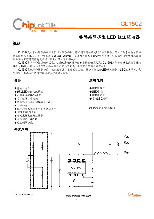
CL1502具有多种恒流辅助功能,实现优异的线性补偿和高精度恒流效果。CL1502工作于电感电流临界连续 模式(TM),输出电流不随电感和负载的变化而变化,具有优异的负载调整特性。
CL1502集成多种保护功能,极大的增强了系统的可靠性。保护功能包括LED开路保护、LED短路保护、欠 压锁定,电流采样电阻短路保护和过温调节功能。
MAX1951ESA-T中文资料

General DescriptionThe MAX1951/MAX1952 high-efficiency, DC-to-DC step-down switching regulators deliver up to 2A of out-put current. The devices operate from an input voltage range of 2.6V to 5.5V and provide an output voltage from 0.8V to V IN , making the MAX1951/MAX1952 ideal for on-board postregulation applications. The MAX1951total output error is less than 1% over load, line, and temperature.The MAX1951/MAX1952 operate at a fixed frequency of 1MHz with an efficiency of up to 94%. The high operating frequency minimizes the size of external components.Internal soft-start control circuitry reduces inrush current.Short-circuit and thermal-overload protection improve design reliability.The MAX1951 provides an adjustable output from 0.8V to V IN , whereas the MAX1952 has a preset output of 1.8V. Both devices are available in a space-saving 8-pin SO package.ApplicationsASIC/DSP/µP/FPGA Core and I/O Voltages Set-Top Boxes Cellular Base StationsNetworking and TelecommunicationsFeatureso Compact 0.385in 2Circuit Footprinto 10µF Ceramic Input and Output Capacitors, 2µH Inductor for 1.5A Output o Efficiency Up to 94%o 1% Output Accuracy Over Load, Line, and Temperature (MAX1951, Up to 1.5A)o Guaranteed 2A Output Current o Operate from 2.6V to 5.5V Supplyo Adjustable Output from 0.8V to V IN (MAX1951)o Preset Output of 1.8V (1.5% Accuracy) (MAX1952)o Internal Digital Soft-Softo Short-Circuit and Thermal-Overload ProtectionMAX1951/MAX19521MHz, All-Ceramic, 2.6V to 5.5V Input,2A PWM Step-Down DC-to-DC Regulators________________________________________________________________Maxim Integrated Products 1Ordering Information19-2622; Rev 1; 8/03For pricing, delivery, and ordering information,please contact Maxim/Dallas Direct!at 1-888-629-4642, or visit Maxim’s website at .Typical Operating CircuitPin ConfigurationM A X 1951/M A X 19521MHz, All-Ceramic, 2.6V to 5.5V Input,2A PWM Step-Down DC-to-DC Regulators 2_______________________________________________________________________________________ABSOLUTE MAXIMUM RATINGSELECTRICAL CHARACTERISTICSStresses beyond those listed under “Absolute Maximum Ratings” may cause permanent damage to the device. These are stress ratings only, and functional operation of the device at these or any other conditions beyond those indicated in the operational sections of the specifications is not implied. Exposure to absolute maximum rating conditions for extended periods may affect device reliability.IN, V CC to GND........................................................-0.3V to +6V COMP, FB, REF to GND.............................-0.3V to (V CC + 0.3V)LX to Current (Note 1).........................................................±4.5A PGND to GND.............................................Internally Connected Continuous Power Dissipation (T A = +85°C)8-Pin SO (derate 12.2mW/°C above +70°C)................976mWOperating Temperature RangeMAX195_ ESA..................................................-40°C to +85°C Junction Temperature Range............................-40°C to +150°C Storage Temperature Range.............................-65°C to +150°C Lead Temperature (soldering, 10s).................................+300°CNote 1:LX has internal clamp diodes to PGND and IN. Applications that forward bias these diodes should take care not to exceedthe IC ’s package power dissipation limits.MAX1951/MAX19521MHz, All-Ceramic, 2.6V to 5.5V Input,2A PWM Step-Down DC-to-DC Regulators_______________________________________________________________________________________3ELECTRICAL CHARACTERISTICS (continued)(V IN = V CC = 3.3V, PGND = GND, FB in regulation, C REF = 0.1µF, T A = 0°C to +85°C , unless otherwise noted. Typical values are at T A = +25°C.)ELECTRICAL CHARACTERISTICSM A X 1951/M A X 19521MHz, All-Ceramic, 2.6V to 5.5V Input,2A PWM Step-Down DC-to-DC Regulators 4_______________________________________________________________________________________Note 3:The LX output is designed to provide 2.4A RMS current.ELECTRICAL CHARACTERISTICS (continued)(V IN = V CC = 3.3V, PGND = GND, FB in regulation, C REF = 0.1µF, T A = -40°C to +85°C , unless otherwise noted.) (Note 2)MAX1951/MAX19521MHz, All-Ceramic, 2.6V to 5.5V Input,2A PWM Step-Down DC-to-DC Regulators_______________________________________________________________________________________5EFFICIENCY vs. LOAD CURRENT(V CC = V IN = 5V)LOAD CURRENT (mA)E F F I C I E N C Y (%)100010010203040506070809010001010,000EFFICIENCY vs. LOAD CURRENT(V CC = V IN = 3.3V)LOAD CURRENT (mA)E F F I C I E N C Y (%)100010010203040506070809010001010,000REF VOLTAGEvs. REF OUTPUT CURRENTREF OUTPUT CURRENT (µA)R E F V O L T A G E (V )35302520151051.9901.9911.9921.9931.9941.9951.98940SWITCHING FREQUENCY vs. INPUT VOLTAGEINPUT VOLTAGE (V)S W I T C H I N G F R E Q U E N C Y (M H z )5.14.63.13.64.10.850.900.951.001.051.101.151.200.802.65.6OUTPUT VOLTAGE DEVIATIONvs. LOAD CURRENTLOAD CURRENT (A)O U T P U T V O L T A G ED E V I A T I O N (m V)1.20.80.4-5-4-3-2-10123456-61.6Typical Operating Characteristics(Typical values are at V IN = V CC = 5V, V OUT = 1.5V, I OUT = 1.5A, and T A = +25°C, unless otherwise noted. See Figure 2.)LOAD TRANSIENT RESPONSEMAX1951 toc0640µs/div0OUTPUT VOLTAGE:100mV/div, AC-COUPLED OUTPUT CURRENT:0.5A/div V IN = 5V V OUT = 2.5V I OUT = 0.5 TO 1ALOAD TRANSIENT RESPONSEMAX1951 toc0740µs/divOUTPUT VOLTAGE:100mV/div, AC-COUPLEDOUTPUT CURRENT:0.5A/div V IN = 3.3V V OUT = 1.5V I OUT = 0.5 TO 1AM A X 1951/M A X 19521MHz, All Ceramic, 2.6V to 5.5V Input,2A PWM Step-Down DC-to-DC Regulators 6_______________________________________________________________________________________Typical Operating Characteristics (continued)(Typical values are at V IN = V CC = 5V, V OUT = 1.5V, I OUT = 1.5A, and T A = +25°C, unless otherwise noted. See Figure 2.)SHUTDOWN CURRENT vs. INPUT VOLTAGEM A X 1951 t o c 12INPUT VOLTAGE (V)S H U T D O W N C U R R E N T (m A )5.04.54.03.53.00.10.20.30.40.50.60.70.80.91.002.55.5SWITCHING WAVEFORMSMAX1951 toc08200ns/div0INDUCTOR CURRENT 1A/divV LX 5V/divOUTPUT VOLTAGE 10mV/div, AC-COUPLEDV IN = 3.3V V OUT = 1.8V I LOAD = 1.5ASOFT-START WAVEFORMSMAX1951 toc091ms/divV COMP 2V/divOUTPUT VOLTAGE 1V/divV IN = V CC = 3.3V V OUT = 2.5V I LOAD = 1.5ASOFT-START WAVEFORMSMAX1951 toc101ms/divV COMP 2V/divOUTPUT VOLTAGE 0.5V/divV IN = V CC = 3.3V V OUT = 0.8VSHUTDOWN WAVEFORMSMAX1951 toc1120µs/divV COMP 2V/divV LX 5V/divOUTPUT VOLTAGE 1V/divV IN = V CC = 3.3V V OUT = 2.5V I LOAD = 1.5AMAX1951/MAX19521MHz, All-Ceramic, 2.6V to 5.5V Input,2A PWM Step-Down DC-to-DC Regulators_______________________________________________________________________________________7Detailed DescriptionThe MAX1951/MAX1952 high-efficiency switching regula-tors are small, simple, DC-to-DC step-down converters capable of delivering up to 2A of output current. The devices operate in pulse-width modulation (PWM) at a fixed frequency of 1MHz from a 2.6V to 5.5V input voltage and provide an output voltage from 0.8V to V IN , making the MAX1951/MAX1952 ideal for on-board postregula-tion applications. The high switching frequency allows for the use of smaller external components, and internal synchronous rectifiers improve efficiency and eliminate the typical Schottky free-wheeling diode. Using the on-resistance of the internal high-side MOSFET to sense switching currents eliminates current-sense resistors,further improving efficiency and cost. The MAX1951total output error over load, line, and temperature (0°C to +85°C) is less than 1%.Controller Block FunctionThe MAX1951/MAX1952 step-down converters use a PWM current-mode control scheme. An open-loop com-parator compares the integrated voltage-feedback signal against the sum of the amplified current-sense signal and the slope compensation ramp. At each rising edge of the internal clock, the internal high-side MOSFET turns on until the PWM comparator trips. During this on-time, cur-rent ramps up through the inductor, sourcing current to the output and storing energy in the inductor. The current-mode feedback system regulates the peak inductor cur-rent as a function of the output voltage error signal. Since the average inductor current is nearly the same as the peak inductor current (<30% ripple current), the circuit acts as a switch-mode transconductance amplifier. To preserve inner-loop stability and eliminate inductor stair-casing, a slope-compensation ramp is summed into the main PWM comparator. During the second half of the cycle, the internal high-side P-channel MOSFET turns off,and the internal low-side N-channel MOSFET turns on.The inductor releases the stored energy as its current ramps down while still providing current to the output. The output capacitor stores charge when the inductor current exceeds the load current, and discharges when the inductor current is lower, smoothing the voltage across the load. Under overload conditions, when the inductor current exceeds the current limit (see the Current Limit section), the high-side MOSFET does not turn on at the rising edge of the clock and the low-side MOSFET remains on to let the inductor current ramp down.Current SenseAn internal current-sense amplifier produces a current signal proportional to the voltage generated by the high-side MOSFET on-resistance and the inductor cur-rent (R DS(ON) x I LX ). The amplified current-sense signal and the internal slope compensation signal are summed together into the comparator ’s inverting input.The PWM comparator turns off the internal high-side MOSFET when this sum exceeds the output from the voltage-error amplifier.Current LimitThe internal high-side MOSFET has a current limit of 3.1A (typ). If the current flowing out of LX exceeds this limit,the high-side MOSFET turns off and the synchronous rectifier turns on. This lowers the duty cycle and causes the output voltage to droop until the current limit is no longer exceeded. A synchronous rectifier current limit of -0.6A (typ) protects the device from current flowing into LX. If the negative current limit is exceeded, the synchro-nous rectifier turns off, forcing the inductor current to flowM A X 1951/M A X 19521MHz, All-Ceramic, 2.6V to 5.5V Input,2A PWM Step-Down DC-to-DC Regulators 8_______________________________________________________________________________________through the high-side MOSFET body diode, back to the input, until the beginning of the next cycle or until the inductor current drops to zero. The MAX1951/MAX1952utilize a pulse-skip mode to prevent overheating during short-circuit output conditions. The device enters pulse-skip mode when the FB voltage drops below 300mV, lim-iting the current to 3A (typ) and reducing power dissipation. Normal operation resumes upon removal of the short-circuit condition.V CC DecouplingDue to the high switching frequency and tight output tolerance (1%), decouple V CC with a 0.1µF capacitor connected from V CC to GND, and a 10Ωresistor con-nected from V CC to IN. Place the capacitor as close to V CC as possible.Soft-StartThe MAX1951/MAX1952 employ digital soft-start circuitry to reduce supply inrush current during startup conditions.When the device exits undervoltage lockout (UVLO), shut-down mode, or restarts following a thermal-overload event, or the external pulldown on COMP is released, the digital soft-start circuitry slowly ramps up the voltages at REF and FB (see the Soft-Start Waveforms in the Typical Operating Characteristics).Undervoltage LockoutIf V CC drops below 2.25V, the UVLO circuit inhibits switching. Once V CC rises above 2.35V, the UVLO clears, and the soft-start sequence activates.Compensationand Shutdown ModeThe output of the internal transconductance voltage error amplifier connects to COMP. The normal operation voltage for COMP is 1V to 2.2V. To shut down the MAX1951/MAX1952, use an NPN bipolar junction transistor or a very low output capacitance open-drain MOSFET to pull COMP to GND. Shutdown mode causes the internal MOSFETs to stop switching, forces LX to a high-impedance state, and shorts REF to G ND.Release COMP to exit shutdown and initiate the soft-start sequence.Thermal-Overload ProtectionThermal-overload protection limits total power dissipation in the device. When the junction temperature exceeds T J = +160°C, a thermal sensor forces the device into shut-down, allowing the die to cool. The thermal sensor turns the device on again after the junction temperature cools by 15°C, resulting in a pulsed output during continuous overload conditions. Following a thermal-shutdown condi-tion, the soft-start sequence begins.Figure 1. Functional DiagramMAX1951/MAX19521MHz, All-Ceramic, 2.6V to 5.5V Input,2A PWM Step-Down DC-to-DC Regulators_______________________________________________________________________________________9Design ProcedureOutput Voltage Selection: Adjustable(MAX1951) or Preset (MAX1952)The MAX1951 provides an adjustable output voltage between 0.8V and V IN . Connect FB to output for 0.8V output. To set the output voltage of the MAX1951 to a voltage greater than V FB (0.8V typ), connect the output to FB and G ND using a resistive divider, as shown in Figure 2a. Choose R2 between 2k Ωand 20k Ω, and set R3 according to the following equation:R3 = R2 x [(V OUT / V FB ) – 1]The MAX1951 PWM circuitry is capable of a stable min-imum duty cycle of 18%. This limits the minimum output voltage that can be generated to 0.18 ✕V IN . Instability may result for V IN /V OUT ratios below 0.18.The MAX1952 provides a preset output voltage.Connect the output to FB, as shown in Figure 2b.Output Inductor DesignUse a 2µH inductor with a minimum 2A-rated DC cur-rent for most applications. For best efficiency, use an inductor with a DC resistance of less than 20m Ωand a saturation current greater than 3A (min). See Table 2for recommended inductors and manufacturers. For most designs, derive a reasonable inductor value (L INIT ) from the following equation:L INIT = V OUT x (V IN - V OUT ) / (V IN x LIR x I OUT(MAX)x f SW )where f SW is the switching frequency (1MHz typ) of the oscillator. Keep the inductor current ripple percentage LIR between 20% and 40% of the maximum load cur-rent for the best compromise of cost, size, and perfor-mance. Calculate the maximum inductor current as:I L(MAX)= (1 + LIR / 2) x I OUT(MAX)Check the final values of the inductor with the output ripple voltage requirement. The output ripple voltage is given by:V RIPPLE = V OUT x (V IN - V OUT ) x ESR / (V IN x L FINAL x f SW )where ESR is the equivalent series resistance of the output capacitors.Input Capacitor DesignThe input filter capacitor reduces peak currents drawn from the power source and reduces noise and voltage ripple on the input caused by the circuit ’s switching.The input capacitor must meet the ripple current requirement (I RMS ) imposed by the switching currents defined by the following equation:For duty ratios less than 0.5, the input capacitor RMS current is higher than the calculated current. Therefore,use a +20% margin when calculating the RMS current at lower duty cycles. Use ceramic capacitors for their low ESR, equivalent series inductance (ESL), and lower cost. Choose a capacitor that exhibits less than 10°C temperature rise at the maximum operating RMS cur-rent for optimum long-term reliability.After determining the input capacitor, check the input ripple voltage due to capacitor discharge when the high-side MOSFET turns on. Calculate the input ripple voltage as follows:V IN_RIPPLE = (I OUT x V OUT ) / (f SW x V IN x C IN )Keep the input ripple voltage less than 3% of the input voltage.Output Capacitor DesignThe key selection parameters for the output capacitor are capacitance, ESR, ESL, and the voltage rating requirements. These affect the overall stability, output ripple voltage, and transient response of the DC-to-DC converter. The output ripple occurs due to variations in the charge stored in the output capacitor, the voltage drop due to the capacitor ’s ESR, and the voltage drop due to the capacitor ’s ESL. Calculate the output voltage ripple due to the output capacitance, ESR, and ESL as:V RIPPLE = V RIPPLE(C)+ V RIPPLE(ESR) + V RIPPLE(ESL)where the output ripple due to output capacitance,ESR, and ESL is:V RIPPLE(C)= I P-P / (8 x C OUT x f SW )V RIPPLE(ESR) = I P-P x ESRV RIPPLE(ESL)= (I P-P / t ON ) x ESL or (I P-P / t OFF ) x ESL,whichever is greater and I P-P the peak-to-peak inductor current is:I P-P = [ (V IN – V OUT ) / f SW x L) ] x V OUT / V INUse these equations for initial capacitor selection, but determine final values by testing a prototype or evalua-tion circuit. As a rule, a smaller ripple current results in less output voltage ripple. Since the inductor ripple current is a factor of the inductor value, the output voltage ripple decreases with larger inductance. Use ceramic capacitors for their low ESR and ESL at the switching frequency of the converter. The low ESL of ceramic capacitors makes ripple voltages negligible.Load transient response depends on the selected output capacitor. During a load transient, the output instantly changes by ESR x I LOAD . Before the controller can respond, the output deviates further, depending on the inductor and output capacitor values. After a short time (see the Load Transient Response graphin theM A X 1951/M A X 19521MHz, All-Ceramic, 2.6V to 5.5V Input,2A PWM Step-Down DC-to-DC Regulators 10______________________________________________________________________________________Typical Operating Characteristic s), the controller responds by regulating the output voltage back to its nominal state. The controller response time depends on the closed-loop bandwidth. A higher bandwidth yields a faster response time, thus preventing the output from deviating further from its regulating value.Compensation DesignThe double pole formed by the inductor and output capacitor of most voltage-mode controllers introduces a large phase shift, which requires an elaborate compensa-tion network to stabilize the control loop. The MAX1951/MAX1952 utilize a current-mode control scheme that reg-ulates the output voltage by forcing the required current through the external inductor, eliminating the double pole caused by the inductor and output capacitor, and greatly simplifying the compensation network. A simple type 1compensation with single compensation resistor (R 1) and compensation capacitor (C 2) creates a stable and high-bandwidth loop.An internal transconductance error amplifier compen-sates the control loop. Connect a series resistor and capacitor between COMP (the output of the error ampli-fier) and G ND to form a pole-zero pair. The external inductor, internal current-sensing circuitry, output capacitor, and the external compensation circuit deter-mine the loop system stability. Choose the inductor and output capacitor based on performance, size, and cost.Additionally, select the compensation resistor and capacitor to optimize control-loop stability. The compo-nent values shown in the typical application circuit (Figure 2) yield stable operation over a broad range of input-to-output voltages.The basic regulator loop consists of a power modulator,an output feedback divider, and an error amplifier. The power modulator has DC gain set by gmc x R LOAD ,with a pole-zero pair set by R LOAD , the output capaci-tor (C OUT ), and its ESR. The following equations define the power modulator:Modulator gain:G MOD = ∆V OUT / ∆V COMP = gmc x R LOAD Modulator pole frequency:fp MOD = 1 / (2 x πx C OUT x (R LOAD +ESR))Modulator zero frequency:fz ESR = 1 / (2 x πx C OUT x ESR)where, R LOAD = V OUT / I OUT(MAX), and gmc = 4.2S.The feedback divider has a gain of G FB = V FB / V OUT ,where V FB is equal to 0.8V. The transconductance error amplifier has a DC gain, G EA(DC),of 70dB. The com-pensation capacitor, C 2,and the output resistance of the error amplifier, R OEA (20M Ω), set the dominantpole. C 2and R 1 set a compensation zero. Calculate the dominant pole frequency as:fp EA = 1 / (2πx C C x R OEA )Determine the compensation zero frequency is:fz EA = 1 / (2πx C C x R C )For best stability and response performance, set the closed-loop unity-gain frequency much higher than the modulator pole frequency. In addition, set the closed-loop crossover unity-gain frequency less than, or equal to, 1/5 of the switching frequency. However, set the maximum zero crossing frequency to less than 1/3 of the zero frequency set by the output capacitance and its ESR when using POSCAP, SPCAP, OSCON, or other electrolytic capacitors.The loop-gain equation at the unity-gain frequency is:G EA(fc) x G MOD(fc) x V FB / V OUT = 1where G EA(fc )= gm EA x R 1, and G MOD(fc)= gmc x R LOAD x fp MOD /f C, where gm EA = 60µS .R 1calculated as:R 1= V OUT x K / (gm EA x V FB x G MOD(fc))where K is the correction factor due to the extra phase introduced by the current loop at high frequencies (>100kHz). K is related to the value of the output capacitance (see Table 1 for values of K vs. C). Set the error-amplifier compensation zero formed by R 1and C 2at the modulator pole frequency at maximum load. C 2is calculated as follows:C 2= (2 x V OUT x C OUT / (R 1 x I OUT(MAX))As the load current decreases, the modulator pole also decreases; however, the modulator gain increases accordingly, resulting in a constant closed-loop unity-gain frequency. Use the following numerical example to calculate R 1and C 2values of the typical application circuit of Figure 2a.Table 1. K ValueV OUT = 1.5VI OUT(MAX)= 1.5A C OUT = 10µF R ESR = 0.010Ωgm EA = 60µSMAX1951/MAX19521MHz, All-Ceramic, 2.6V to 5.5V Input,2A PWM Step-Down DC-to-DC Regulators______________________________________________________________________________________11gmc = 4.2Sf SWITCH = 1MHzR LOAD = V OUT / I OUT(MAX)= 1.5V / 1.5 A = 1Ωfp MOD = [1 / (2πx C OUT x (R LOAD + R ESR )]= [1 / (2 x π×10 ×10-6x (1 + 0.01)] = 15.76kHz.fz ESR = [1/(2πxC OUT R ESR )]= [1 / (2 x π×10 ×10-6×0.01)] = 1.59MHz.For 2µH output inductor, pick the closed-loop unity-gain crossover frequency (f C ) at 200kHz. Determine the power modulator gain at f C :G MOD(fc )= gmc ×R LOAD ×fp MOD / f C = 4.2 ×1 ×15.76kHz / 200kHz = 0.33then:R 1= V O x K / (gm EA x V FB x G MOD(fc )) = (1.5 x 0.55) /(60 ×10-6 ×0.8 ×0.33) ≈51.1k Ω(1%)C 2= (2 x V OUT ×C OUT ) / (R C ×I OUT(max))= (2 ×1.25 × 10 × 10-6)/ (51.1k ×1.5) ≈209pF, choose 220pF, 10%Applications InformationPC Board Layout ConsiderationsCareful PC board layout is critical to achieve clean and stable operation. The switching power stage requires particular attention. Follow these guidelines for good PC board layout:1)Place decoupling capacitors as close to the IC as possible. Keep power ground plane (connected to PG ND) and signal ground plane (connected to GND) separate.2)Connect input and output capacitors to the power ground plane; connect all other capacitors to the signal ground plane.3)Keep the high-current paths as short and wide as possible. Keep the path of switching current (C1 to IN and C1 to PG ND) short. Avoid vias in the switching paths.4)If possible, connect IN, LX, and PGND separately to a large copper area to help cool the IC to further improve efficiency and long-term reliability.5)Ensure all feedback connections are short and direct. Place the feedback resistors as close to the IC as possible.6)Route high-speed switching nodes away from sensi-tive analog areas (FB, COMP).Thermal ConsiderationsThe MAX1951 uses a fused-lead 8-pin SO package with a R THJC rating of 32°C/W. The MAX1951 EV kit layout is optimized for 1.5A. The typical application circuit shown in Figure 2c was tested with the existing MAX1951 EV kit layout at +85°C ambient temperature, and G ND lead temperature was measured at +113°C for a typical device. The estimated junction temperature was +138°C. Thermal performance can be further improved with one of the following options:1) Increase the copper areas connected to G ND, LX,and IN.2) Provide thermal vias next to G ND and IN, to the ground plane and power plane on the back side of PC board, with openings in the solder mask next to the vias to provide better thermal conduction.3) Provide forced-air cooling to further reduce case temperature.M A X 1951/M A X 19521MHz, All-Ceramic, 2.6V to 5.5V Input,2A PWM Step-Down DC-to-DC Regulators 12______________________________________________________________________________________Figure 2a. MAX1951 Adjustable Output Typical Application CircuitFigure 2b. MAX1952 Fixed-Output Typical Application CircuitMAX1951/MAX19521MHz, All-Ceramic, 2.6V to 5.5V Input,2A PWM Step-Down DC-to-DC Regulators______________________________________________________________________________________13Figure 2c. MAX1951 Typical Application Circuit with 2A OutputM A X 1951/M A X 19521MHz, All-Ceramic, 2.6V to 5.5V Input,2A PWM Step-Down DC-to-DC Regulators 14______________________________________________________________________________________Chip InformationTRANSISTOR COUNT: 2500PROCESS: BiCMOSMAX1951/MAX19521MHz, All-Ceramic, 2.6V to 5.5V Input,2A PWM Step-Down DC-to-DC RegulatorsMaxim cannot assume responsibility for use of any circuitry other than circuitry entirely embod ied in a Maxim prod uct. No circuit patent licenses are implied. Maxim reserves the right to change the circuitry and specifications without notice at any time.Maxim Integrated Products, 120 San Gabriel Drive, Sunnyvale, CA 94086 408-737-7600 ____________________15©2003 Maxim Integrated ProductsPrinted USAis a registered trademark of Maxim Integrated Products.Package Information(The package drawing(s) in this data sheet may not reflect the most current specifications. For the latest package outline information go to /packages .)。
3.7V转3.3V,3.7V转1.5V芯片,PW2058和PW2059规格书
0.8A,同步降压转换器一般说明自动英文翻译篇PW2058/PW2059是一种恒频、电流模式降压转换器。
该器件集成了一个主开关和一个同步整流器,无需外加肖特基二极管就可以实现高效率。
它是用单电池锂离子电池为便携式设备供电的理想选择。
输出电压可调低至0.6V,PW2058/PW2059还可在100%的占空比下进行低电压降操作,延长了便携式系统的电池寿命。
该装置提供PWM控制和PFM模式开关控制两种工作模式,可在更宽的负载范围内实现高效率。
特征⚫效率高达96%⚫ 1.5MHz恒频运行⚫ 800mA输出电流⚫不需要肖特基二极管⚫ 2V至6V输入电压范围⚫输出电压低至0.6V⚫低负载下高效率的PFM模式⚫退出运行时100%占空比⚫低静态电流:20μA⚫斜坡补偿电流模式控制,以获得良好的线路和负载瞬态响应⚫短路保护⚫热故障保护⚫涌流限制和软启动⚫ <1μA关断电流⚫ SOT23-5包应用⚫移动电话和智能手机⚫无线和DSL调制解调器⚫ PDA系统⚫便携式仪器⚫数码相机和摄像机⚫数字电视典型应用电路芯片135代2845理8039 Mr。
郑,有技术FAE支援引脚分配/说明PCB布局建议布置印刷电路板时,应进行以下检查,以确保PW2058/PW2059正常工作。
在布局中检查以下内容:1.功率轨迹,包括GND轨迹、SW轨迹和Vin轨迹应保持短、直、宽。
2.CIN的(+)板是否尽可能靠近车辆识别号(VIN)。
这个电容器为内部功率mosfet提供交流电流。
3.使交换节点SW远离敏感的VOUT节点。
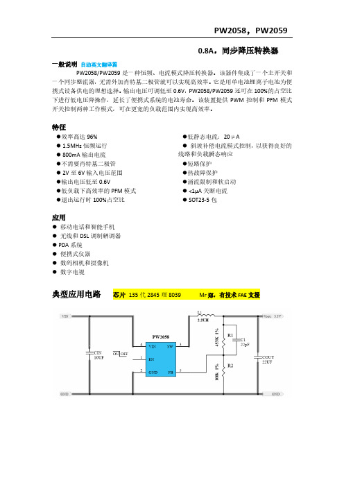
4.尽可能靠近CIN和COUT的(-)板功能描述PW2058/PW2059是一款高性能、800mA、1.5MHz单片降压转换器。
PW2058/PW2059只需要三个外部电源部件(CIN、COUT和L)。
可调版本可编程的外部反馈任何电压,从0.6V到输入电压。
在下降操作时,转换器占空比增加到100%,输出电压跟踪输入电压减去高压侧MOSFET的RDS(ON)降。
LM2653 1.5A 同步切换电源评估板用户指南说明书

User'sGuideSNVA012B–May1999–RevisedApril2013
AN–1133LM2653EVAL1.5ASynchronousSwitchingRegulatorEvaluationBoard
1IntroductionTheLM2653switchingregulatorprovideshighefficiencypowerconversionovera100:1loadrange(1.5Ato15mA).ThisfeaturemakestheLM2653anidealfitinbattery-poweredapplications.
Synchronousrectificationand75mΩinternalswitchesprovideupto97%efficiency.Atlightloads,theLM2653entersalowpowerhystereticor“sleep”modetokeeptheefficiencyhigh.Inmanyapplications,theefficiencystillexceeds80%at15mAload.AshutdownpinisavailabletodisabletheLM2653andreducethesupplycurrentto7µA.
TheICcontainspatentedcurrentsensingcircuitryforcurrentmodecontrol.Thisfeatureeliminatestheexternalcurrentsensingrequiredbyothercurrent-modeDC-DCconverters.
TheIChasa300kHzfixedfrequencyinternaloscillator.Thehighoscillatorfrequencyallowstheuseofextremelysmall,lowprofilecomponents.
泰姬尔电子Ultima 150电源产品说明书

Quick Change Torch! No tools required.Cost Savings! The Ultima 150 is priced competitively with automated TIG systems. Plasma welding ismeasurably the lower cost process with savings gained through increased productivity, reduced scrap, reduced down time and fewer electrode changes.Wide Current Range!0.5 – 150amp current range for quality performance over a wide variety of applications.Very Smooth Arc! Ultra smooth DC arc for repetitive, high quality welds.Repeatable Arc Starting! Pilot arc allows for repeatable arc starts,reducing defects and rework.Multiple Voltage! 208-460 VAC in 1 or 3 phase power at 50 or 60 Hz with 575 VAC optional module.Simple to Set-Up! The Ultima 150is a self contained unit, which requires attaching input power and gasses, then mounting the torch.Smart Logic ®! Prevents damage to the internal components if installed to improper voltage.Current Limiter! Limits power source output to torch capability to avoid torch damage.Preview Set Current! Allows you to display actual current/voltage and avoid costly test set-ups.Easy to Use! Simple interface for automated or manual control.*Limited warranty. Refer to warranty schedule.**Refer to ordering information for torch selection.#Subject to change without notification.5 Y e a r*Repeatable welds again, and again, and again#Subject to change without notification.What is Plasma Welding?#Plasma Welding is a superior variation of the TIG process that offers many advantages over TIG:•Increases productivity by reducing down time•Reduces scrap by providing consistent arc starting every time •Improved process control for repeatable, high quality welds •Reduces interference (noise) with computers, phone systems,CNC controllersSimply stated, plasma welding is a variation to GTAW (TIG) that encloses the tungsten electrode in a protected environment (Fig. 1) and delivers the arc through a cooled copper tip.Enclosing the electrode protects it from contamination, thus substantially extending electrode life. The consistent arcshape of plasma results in consistent welds for 8 hours or more of operation as compared to automated TIG welding, where deterioration of the exposed TIG electrode (Fig. 2) can result in weld arc variations (Fig. 3) in one hour or less of operation.Plasma welding uses a pilot arc (Fig. 4) to consistently transfer the arc to the work without the repeated use of high frequency current. The Ultima 150 pilot arc circuit results in repetitive starting and reduces problems of high frequency interference with CNC controls, phones and computers which are commonwith the TIG process.PilotProtected ElectrodeFigure 1Figure 2Figure 3Figure 4Tig Weld SampleUsed Tig ElectrodeNew ElectrodeUsed Plasma ElectrodeTIGPLASMAShift Hours per Day 24Days worked per Week5Value Per Part:1Production Parts/Dollars Gained with Plasma:94,640Typical Plasma/TIG Welding Productivity Benefit AnalysisTotal Parts Tig Electrode Minutes to Parts Lost Plasma ElectrodeParts Lost Net Gain PlasmaTimeat 100% Cap.ChangesChange Electrodewith TIGChangeswith Plasmaover TIGHour 20815170017Day 4,99224120416352364Week 24,9601206002,080152601,820Month 108,1605202,6009,013651,1277,887Year1,297,9206,24031,200108,16078013,52094,640Application: Outside corner welds home applianceNote: 4 welds required on each part. For more information, contact Thermal Arc or your Authorized Thermal Arc Distributor.Plasma & Secondarygas flow meter.Quick disconnect hand held orautomated torchesavailable.Easy fill coolantreservoir with built-in deionizer bag.Features##Subject to change without notification.System status anderror indicator lights.Digital welding/Pilot current amp meter.Specifications ##Subject to change without notification.®Control Panel#2.Shield Gas Flow Control3.Plasma Gas Flow Control4.Pilot Arc On/Set5.Pilot Current Adjust6.Pilot Current Preview7.Weld Current Preview/Actual 8.Weld Current Adjust 9.Current Limiter Adjust10.Weld Current Range 11. Remote/Panel ControlPANEL INDICATOR LIGHTS 1.AC - indicates correct input voltage is applied2.TEMP - over temperature indicator light3.Gas - lights to indicate Plasma & Shield gas pressure switches are satisfied4.Coolant - indicates proper coolant flow to torch5.Pilot - indicates pilot arc is active6.DC - indicates output welding DC current is active123567891011#Subject to change without notification.4123456Torch Specifications#2-2130 (M)NOTE: All torches listed incorporate a quick disconnect connector specifically for operation with the Ultima 150.(H) designates torch with molded handle(M) designates torch with rack and pinion assembly#Subject to change without notification.Torch Parts#SPARE SPARE SPAREPARTS PARTS PARTS ITEM PART2A KIT3A KIT4A KIT NO.DESCRIPTION TORCH5-2984TORCH5-2985TORCH5-29861Torch Head8-2027 (70°)8-3030 (70°))8-4014 (70°) Assembly8-2028 (90°)8-3031 (90°)8-4015 (90°)8-2097 (180°offset)8-3032 (180°offset)8-4016 (180°offset)8-4054 (180°inline) 2Shield Cup8-3236 (use w/ext. tip)28-304018-408818-2071 (use w/std. tip)3Tip8-2023 (.045) 35A-std9-1788 (.031) 35A-lg9-1890 (.062) 100A-lg58-2024 (.062) 55A-std9-1789 (.046) 50A-lg59-1891 (.093) 125A-lg58-2025 (.081) 75A-std9-1790 (.062) 75A-lg9-1892 (.125) 150A-lg*58-2079 (.031) 15A-lg9-1791 (.081) 100A-lg58-2080 (.045) 25A-lg9-1811 (.-093) 130A-lg58-2082 (.062) 35A-lg58-2083 (.081) 50A-lg54Electrode8-2033 (.093) std8-2007 (.093) std.29-1827 (.187) std.28-2006 (.093) ext.9-1775 (.093) ext.9-1834 (.187) ext.8-2044 (.040) std.8-2046 (.040) ext.5Liner N/A N/A8-40112 6Gas Distributor8-2040 (.093-electrode)19-224019-22041 (insulating sleeve)8-2042 (.040-electrode)7Gas Diffuser N/A8-30598-40878Collet Assembly8-2039 (.093-electrode)9-178019-18768-2041 (.040-electrode)9Back Cap8-2032 (std-electrode)9-1779 (std-electrode)8-4158 (std-electrode)8-2030 (ext-electrode)9-1803 (ext-electrode)9-1877 (ext-electrode)N/S Collar N/A N/A8-4024N/S O-ring (liner)N/A N/A8-0560N/S O-ring (internal)N/A N/A8-0528N/S O-ring (back-cap)8-20358-05278-0530N/S Gasket (shield cup)8-20368-30578-4069N/S Gage/Wrench Assy8-202119-181019-18731N/S Lubricant8-402518-402518-40251N/S Tool Box8-314118-314118-31411 NOTE:The use of extended electrode requires an extended back cap.Tip ratings @ minimum electrode setback.*Tip maximum current rating not to exceed the maximum output of Ultima-150#Subject to change without notification.Ordering InformationPRODUCT PART NO.DESCRIPTION QTY PRICE Ultima 1503-2770Power source only inc. quick disconnect assemblyPART NO.PART NO.SYSTEMw/12.5ft torch & leads w/25ft torch & leads DESCRIPTIONUltima 150 System Torch (rating)2A(75 Amps)1-1551-211-1552-21PWH-2A, 70 degree1-1551-221-1552-22PWH-2A, 90 degree1-1551-231-1552-23PWH-2A, 180 degree1-1553-231-1553-23PWM-2A, 180 degree3A(150 Amps)1-1551-311-1552-31PWH-3A, 70 degree1-1551-321-1552-32PWH-3A, 90 degree1-1551-331-1552-33PWH-3A, 180 degree1-1553-331-1553-33PWM-3A, 180 degree4A(200 Amps)1-1551-411-1552-41PWH-4A, 70 degree1-1551-421-1552-42PWH-4A, 90 degree1-1551-431-1552-43PWH-4A, 180 degree1-1551-531-1552-53PWH-4A1, 180 degree1-1553-431-1553-43PWM-4A, 180 degree1-1553-531-1553-53PWM-4A1, 180 degreeACCESSORIES PART NO.DESCRIPTIONQuick Disconnect Kit5-2990Allows existing torches to be converted for use with Ultima 150Regulator - Argon9-2722Regulator - Argon/Hydrogen9-3053Foot Control7-3080Hand Pendant10-2005Requires 7-3316 adapterRemote Interface Cable 10ft.9-4063Weld Process Controller - WC-1600279Remote Hand Pendant 25ft.600280Cable Assembly (required for WC-1)9-4129TOTAL QUOTE PRICENOTE: PWH designates a torch with a molded handle; PWM designates a torch with rack and pinion.Torch amperage rating based on minimum electrode set back.。
简易低价电源控制器:SC2618说明书

应用在电子消费产品上的低价简易电源控制器Chen ZhouSemtech International AG, ShanghaiAbstract: 随着新一代机顶盒, 高清晰度电视进入普通家庭,此类产品的销售价格将进一步下降。
如何降低此类产品成本是许多开发工程师重要的任务之一。
在这篇文章中将介绍一种简易低价电源控制器(SC2618)。
它5V,12V,和24V输入消费电子产品中有较好的应用。
Abstract: As new consumer electronics products such as set-top-boxes, digital high definition TVs, xDSL modems are becoming mainstream electronics items in ordinary homes, selling price of these products are decreasing significantly. This places tremendous pressure on electronic designers to lower overall product cost. In this paper, a simple low cost synchronous buck PWM controller SC2618 is introduced. It is found that the simplicity and functionality of SC2618 enable wide usages in today’s consumer power supply applications.Keywords: PWM Controller, Synchronous BuckI. 引言过去电子设计工程师通常向电源生产厂家购买交流转直流开关电源。
这种电源通常需要带有多组输出隔离变压器并由一颗原边电源控制器控制输出电压和电流。
IR1167智能同步整流控制器
所示) ,保证在关断后的消隐时间内不做动作。当 VDS 达到 VTH3 后,消隐时间结
束,IR1167 复位,为下一个开关周期做好准备。
AN-1087
5
ID_PRIM VDS_PRIM
T1 ID_SEC VDS_SEC
T2
T3
ID_PRIM VDS_PRIM
图 5: 断续模式波形示意
图 13: 中心抽头低侧整流 (半桥或全桥), 辅助绕组供电 (Voutput < 6V)。
IR1167
Rmot
Vd
EN
Vs
MOT
Rg
GND OVT
Vgate Vcc
C
R C
Vgate Vcc
Rg
GND OVT
Vs
MOT
Vd
EN
IR1167
Rmot
+ -
OUTPUT
图 14: 中心抽头低侧整流 (半桥或全桥), 绕组抽头供电 (6V < Voutput < 10V)。
AN-1087
3
开关管导通后源极到漏极电压下降到 RDSon ⋅ ID ,而且此时变压器漏感和初级开关管 输出电容之间会产生寄生震荡,导致整流开关管上有电压振铃而会令VDS电平下降 到VTH1, 可能导致误关断。所以IR1167芯片内部采用专用逻辑电路(MOT和tblank) 防止抖动引起的误关断和导通,这将在后文中详细介绍。
fSWmax = 66.14 + 3⋅ 2.48 = 73.6kHz
¾ 工作模式 全范围改变交流输入和负载,可以看到电源工作在哪种模式。
AN-1087
15
设计要点
以下计算是假定同步整流开关管和上文的几个系统参数都已经获取的情况。 a. OVT 设置
LLC用同步整流管MDU1511
ID, Drain Current [A]
2
100 ms
100 90 80 70 60 50 40 30
10
1
DC
10
0
10
-1
Single Pulse TJ=Max Rated TC=25℃
20 10
10
-2
10
-1
10
0
10
1
10
0 25
50
75
100
125
150
VDS, Drain-Source Voltage [V]
6
2500 2000 1500 1000 500 0
※ Notes ; 1. VGS = 0 V 2. f = 1 MHz
4
2
Coss Crss
0 5 10 15 20
0 0 5 10 15 20 25 30 35 40 45 50 55
25
QG, Total Gate Charge [nC]
VDS, Drain-Source Voltage [V]
Characteristics Drain-Source Voltage Gate-Source Voltage TC=25 C Continuous Drain Current (1) TC=70 C TA=25 C TA=70oC Pulsed Drain Current TC=25 C TC=70 C Power Dissipation TA=25 C TA=70oC Single Pulse Avalanche Energy (2) Junction and Storage Temperature Range EAS TJ, Tstg
38.8 18.7 2510 246 490 -
AE1501 PWM降压型DC DC开关调节器 技术说明书 V1.0
PWM降压型DC/DC开关调节器◆主要特征◆ 概述– 3.3V,5V两种固定输出电压型–内置固定频率为150kHz的振荡器–过热保护电路和限流保护电路–输入电压最高到36V–只需4个外围器件–可提供3A负载电流–待机电流85uA–高效率◆ 应用领域- 简单的高效降压调节器–LCD电压调节器◆ 管脚设置5-Lead TO-263(S)AE1501系列是降压型开关稳压器,具有优良的电压调整率和负载调整率。
能够提供3A的负载电流。
有3.3V、5V两种固定输出电压型。
外围元件少,应用简单,内置频率补偿电路和固定频率振荡器。
开关频率为150KHz,可以使用小尺寸的滤波元件。
在额定输入电压和输出负载的条件下,输出电压容差为±5%,振荡频率的容差为±15%。
待机电流为85μA(典型值),内置两级过流保护电路和过热保护电路。
◆功能框图◆ 最大绝对额定值◆ 电气特性除非特别说明,V IN=12V, I LOAD=500mA。
◆ 电气特性(续)==注1:最大绝对额定值给器件的正常工作范围做了限制,超过这些条件时器件有可能损坏。
注2:人体放电模式相当于一个100pF 的电容通过一个1.5KΩ的电阻向每个管脚放电。
注3:典型数据是指在工作在25℃下,代表最常见的情况。
注4:所有的范围保证在室温和极限温度下,所有室温下的范围都是经过100%测试得出的,所有的极限温度下的范围都可以通过使用相关的标准统计质量控制方法来加以保证。
注5:外部元件为续流二极管、储能电感、输入和输出端电容,会影响开关调节器的系统性能,AE1501用在如图1所示测试电路中时,其系统性能如电气特性中的系统参数所示。
注6:当第二级电流限制起作用时,开关频率会降低,降低值决定于过流程度。
注7:输出脚不连接二极管、电感和电容。
注8:把反馈端直接连接到0V 电压,强制输出开关管常开启。
注9:把连接在调整器输出脚的反馈端断开,V OUT =3.3V、5V 的AE1501反馈端连接12V 电压,强制输出开关管常关闭。
MAX31865中文资料_数据手册_参数
VIL
CS, SDI, SCLK
Input Logic 1
Analog Voltages (FORCE+,FORCE2, FORCE-, RTDIN+, RTDIN-) Reference Resistor Cable Resistance
VIH
CS, SDI, SCLK
Normal conversion results
MAX31865 RTD-to-Digital Converter
ABSOLUTE MAXIMUM RATINGS
Voltage Range on VDD Relative to GND1.............-0.3V to +4.0V Voltage Range on BIAS, REFIN+,
Applications
Industrial Equipment Medical Equipment Instrumentation
Ordering Information appears at end of data sheet.
For related parts and recommended products to use with this part, refer to /MAX31865.related.
PACKAGE THERMAL CHARACTERISTICS (Note 1)
TQFN Junction-to-Ambient Thermal Resistance (qJA)...........29°C/W Junction-to-Case Thermal Resistance (qJC)..................2°C/W
EVALUATION KIT AVAILABLE
- 1、下载文档前请自行甄别文档内容的完整性,平台不提供额外的编辑、内容补充、找答案等附加服务。
- 2、"仅部分预览"的文档,不可在线预览部分如存在完整性等问题,可反馈申请退款(可完整预览的文档不适用该条件!)。
- 3、如文档侵犯您的权益,请联系客服反馈,我们会尽快为您处理(人工客服工作时间:9:00-18:30)。
MAX15026 同步降压控制器
MAX15026 同步降压控制器工作在 4.5V 至 28V 输入电压范围内,可产生
调节范围为输入电压的 85%到低至 0.6V 的输出电压,支持高达 25A 的负载电
流。器件允许单调启动至预偏置而不对输出放电,并具有自适应的内部数字软
启动功能。 MAX15026 可通过外部电阻在 200kHz 至 2MHz 范围内调节开
关频率。MAX15026 的自适应同步整流无需外部续流肖特基二极管。该器件用
外部低边 MOSFET 的导通电阻作为电流检测元件,省去了电流检测电阻。这
样无需检流电阻即可在输出过载或输出短路故障情况下保护 DC-DC 元件不受
损坏。打嗝模式限流降低了短路情况下的功耗。MAX15026 包括一个电源就绪
输出和一个具有精确开启/关断门限的使能输入,可用于输入电源监测和电源排
序。
其它保护功能包括吸电流模式限流及热关断。
当器件从输出吸电流时,吸电流模式限流功能可防止反向电感电流达到
危险值。
MAX15026 采用节省空间和热增强型 3mm x 3mm、14 引脚 TDFN-EP 封
装。MAX15026 可工作在扩展级-40°C 至+85°C 以及汽车级-40°C 至+125°C 温
度范围。
关键特性
4.5V 至 28V 或 5V ±10%输入电压范围
0.6V 至(0.85 x VIN)可调输出
200kHz 至 2MHz 可调开关频率
可启动至预偏置负载
具有可调温度补偿门限的无损、逐周期、谷电流模式限流