A 0.8V 64×64 CMOS imager with integrated sense-and-stimulus pixel for artificial retina
Leon Instruments X3-DIL64 原型板用户指南说明书

X3-DIL64 prototyping modulewith ATxmega128A3U-AU processorLeon Instrumentswww.leon-instruments.plversion 2.1X3-DIL64 prototyping module allows rapid development of electronic equipment with low cost and advanced ATxmega128A3U microcontroller by Atmel. The module is intended to be used in design offices, school laboratories and for hobbyists.G e n e r a l d e s c r i p t i o nThe X3-DIL64 module is populated with:∙ATxmega128A3U-AU microcontroller∙MiniUSB connector∙MicroSD card socket∙PDI programming interface connector∙Crystal oscillator socket∙RESET button and button for enabling USB programming mode∙Voltage regulator and filtersA b s o l u t e m a x i m u m r a t i n g sStresses exceeding absolute maximum ratings reduce device reliability and may cause perma-nent damage to the device.Other parameters are listed in ATxmega128A3U datasheet.S TORAGE AND H ANDLINGStatic electricity can significantly shorten the lifespan of electronic components. Please observe these tips to prevent damage that could occur from electro-static discharge: ∙Use anti-static precautions such as operating on an anti-static mat and wearing an anti-static wrist-band.∙Store the evaluation board in the packaging provided.∙Touch a metal USB housing to equalize voltage potential between you and the board.A T x m e g a128A3U m i c r o c o n t r o l l e rGeneral description of the microcontroller’s functionality and parameters:∙Memory: 128kB Flash, 8kB SRA, 2kB EEPROM∙Four-channel DMA controller∙Eight-channel event system∙Seven programmable timers/counters∙Full-speed USB∙Seven USARTs with IrDA support for one USART∙Two two-wire interfaces with dual address match (I2C and SMBus compatible)∙Three serial peripheral interfaces (SPIs)∙AES and DES crypto engine∙CRC-16 (CRC-CCITT) and CRC-32 (IEEE® 802.3) generator∙Two sixteen-channel, 12-bit, 2msps Analog to Digital Converters∙One two-channel, 12-bit, 1msps Digital to Analog Converter∙Four Analog Comparators with window compare function, and current sources∙External interrupts on all general purpose I/O pins∙Programmable watchdog timer with separate on-chip ultra low power oscillator∙QTouch® library supportCPU C LOCK F REQUENCY32MHz at 2,7V; 12MHz at 1,6V.The microcontroller is equipped with an internal RC oscillator, providing CPU clock without the need of external crystal connection. Internal RC oscillator is enabled as default. Maximum fre-quency of crystal oscillator is 16MHz.For further information please refer to ATxmega128A3U datasheet.X3-D I L64U s e r’s G u i d eThe module components are listed in the figure 1.Fig. 1. X3-DIL64 componentsP OWERX3-DIL module can be powered in many ways:1)MiniUSB connector– connect the module to your computer with a MiniUSB cable. Put theUSBPWR jumper on. You can measure USB bus voltage with a voltmeter connected to 5V/GND.2)5V/GND connector– apply 5V voltage to 5V/GND connector and put the USBPWR jumperon. In this case connection to a computer via MiniUSB is not allowed.3)PDI programmer connector– if your programmer provides powering the programmed cir-cuit, the X3-DIL64 module can be powered from PDI connector. Take the USBPWR jumper off. Connection to a computer via MiniUSB is possible.4)Any 3V3 and GND pin on edge connector– apply 3.3V voltage to any pin signed 3V3 andconnect any GND pin to the ground. All 3V3 and GND pins are joined together so there’s no need to join them manually. The USBPWR jumper should be taken off. Connection to a computer via MiniUSB is possible.Regardless of the powering method, on all 3V3 pins should be measured 3.3V. Improper configura-tion of the USBPWR jumper may cause permanent damage to the X3-DIL64 module and/or other equipment.M EMORY P ROGRAMMINGATxmega128A3U has internal 128kB flash memory to store software and 2kB EEPROM for user data. You can access these memories with following tools:1.Programmer compatible with PDI standard–example of this kind programmer is Atmel’sAVR ISPmkII. Pinout of PDI connector is shown in figure 2.Fig. 2. PDI connector pinout1)FLIP bootloader– the microcontroller populated in X3-DIL64 module is programmed withFLIP bootloader to make possible memory programming without PDI programmer. FLIP loader is available at /tools/FLIP.aspx and should be installed on your computer. To enter the programming mode, press and hold RESET and FLIP button.Then release RESET and your computer should immediately recognize a new USB device.Next, release FLIP button. Now ATxmega128A3U is in programming mode and ready to download new software from the computer.2)JTAG interface– there is no JTAG connector on X3-DIL64 board but ATxmega128A3U sup-ports this interface. Connect JTAG programmer to TDO, TCK, TDI, TMS pins.Do not disconnect power or programming cable while the downloading process is in progress be-cause it may damage the microcontroller.USB I NTERFACEATxmega128A3U supports full-speed USB 2.0 interface. USB signal lines are connected to following processor I/O pins:∙D+– pin D7∙D–– pin D6Anti-spike 22R resistors are placed between the USB connector and the microcontroller.M ICRO SD C ARD S OCKETX3-DIL64 is populated with a MicroSD card socket. MicroSD uses SPI interface connected as fol-lows:∙MISO– pin C6∙MOSI– pin C5∙SCK– pin C7∙CS– pin C4∙CARD-DETECT– pin E0After MicroSC card insertion, pin E0 is shorted to ground with 470R resistor. In case the user doesn’t have MicroSD it is possible to use port C for other purpose but the socket must be empty.FLIP B UTTONFLIP button is designed to switch the microcontroller into memory programming mode but it can be used as general purpose button for user’s applications. When pressed, it shorts E5 pin to the ground. Pin E5 is pulled-up with a 100k resistor.FLIP– pin E5C RYSTAL O SCILLATOR S OCKETX3-DIL64 module supports fast and easy crystal oscillator replacement without the need of solder-ing. Just plug the oscillator into the socket. HC49 type crystals are compatible with the socket. Maximum frequency of crystal oscillator is 16MHz.D UAL-I N-L INE C ONNECTORSX3-DIL64 module has two 32-pin connectors on the both edges of the board. The placement and dimensions of these connectors were designed to be identical as standard DIL64 package. Num-bers of TQFP64 pins package are same as DIL64 package and placed in the same order.D e m o n s t r a t i o n S o f t w a r eATxmega128A3U is pre-programmed with a demonstration program. The processor generates low frequency square signals on port F. When FLIP button pressed, the frequency of these signals dou-bles. You can observe this using a LED diode with 470R serial resistor connected between any port F pin and the ground or to any other port F pin.#include<avr/io.h>#include<util/delay.h>int main(void){PORTE.DIR=0;// port E as inputPORTF.DIR=0b11111111;// port F as outputuint8_t counter=0;// to control blinking LEDswhile(1){counter++;PORTF.OUT=counter;if(PORTE.IN&(1<<5)){// if FLIP pressed_delay_ms(100);}else{// if FLIP released_delay_ms(50);}}}This and other demonstration designs are available at http://www.leon-instruments.pl.T e c h n i c a l D r a w i n gR e v i s i o n H i s t o r y。
RTC6711
SYMBOL
PARAMETER
CONDITION
Tj VDD2D5 VDD33
I_RF
I_module
I_pd Fref V_IH
V_IL
Temperature Range Analog Supply Voltage
3.3V Supply Voltage Power consumption for IC
31 VAMPVDD 30 VAMPIN
29 BBOUT2
Buffer
VDD33D 9
SPI
VSS_SYN3 10
Synthesizer
Buffer AGC
28 VAMP_REF 27 FSKCOMIN
VSS_SYN4 11
26 BBVDD0
XTAL1 12
25 AGC_C
13 14 15 16 17 18 19 20 21 22 23 24
Preliminary
38 FSKVDD 39 HYS_C
40 FSKCOMOUT 41 BBVDD1 42 IFAOUTN 43 IFAOUTP 44 VDD33_IFA 45 IFAVDD 46 RFGND 47 RFIN 48 LNA_LG
Block Diagram
Data Sheet
RTC6711
Supply IN Digital Control Input Digital Control Input Analog I/O
AD9783中文资料

CLKP CLKN
LVDS INTERFAቤተ መጻሕፍቲ ባይዱE
D[15:0] VIA, VIB
DEINTERLEAVING LOGIC
Full programmability is provided through a serial peripheral interface (SPI) port. Some pin-programmable features are also offered for those applications without a controller.
Dual 12-/14-/16-Bit,
LVDS Interface, 500 MSPS DACs
AD9780/AD9781/AD9783
GENERAL DESCRIPTION
The AD9780/AD9781/AD9783 include pin-compatible, high dynamic range, dual digital-to-analog converters (DACs) with 12-/14-/16-bit resolutions, and sample rates of up to 500 MSPS. The devices include specific features for direct conversion transmit applications, including gain and offset compensation, and they interface seamlessly with analog quadrature modulators such as the ADL5370.
A 6-μW Chip-Area-Efficient Output-Capacitorless LDO in 90-nm CMOS Technology

With forecasting that more SoC will be implemented by ultra-small-scale technologies in the next decade, the impacts, either positive or negative, of the nano-scale technology on the OCL-LDO design cannot be overlooked anymore. Unfortunately, most of the foregoing OCL-LDO designs are not implemented in nano-scale technologies, except one fully-integrated 50-mA LDO design implemented in 90-nm CMOS technology reported in 2005 [3]. This design consumes a quiescent current of 6 mA and is stabilized by a 0.6-nF on-chip capacitor. The load regulation under voltage positioning is 90 mV/50 mA. The performance of this LDO design reveals that the design challenges of OCL-LDO in nano-scale technology are (1) enhancement of loop gain for better load regulation, (2) optimization of quiescent current for power saving, and (3) minimization of on-chip capacitance for chip-area reduction. The recently reported OCL-LDO structures are based on a LDO reported in [3], [7], [10] and [11], as shown in Fig. 1. The core is a flipped voltage follower (FVF) [12]. The stability of this LDO structure has been proven stable under the absence of an off-chip capacitor. However, the large-signal response under the lowcondition limits the transient response, and thus dynamic biasing was proposed in [7] and [11]. When the LDO is implemented in nano-scale technology, both the small-signal and large-signal responses are expected to be significantly improved due to the much smaller parasitic capacitance associated with nano-devices. However, the FVF-based LDO structure itself does not have a high loop gain due to its simple folded circuit structure, even though it is implemented in a submicron CMOS technology. As a result, the reported load regulation is not outstanding. It can be easily predicted that when
sp0829spec_commercial 2.0

1/15 Inch QVGA CMOS Image SensorSP0829SpecificationVersion Commercial 2.02012.01.16SuperPix Micro Technology Co., LtdS up er P i xSP 08291/15 Inch QVGA CMOS Image Sensor Part Number SP0829SuperPix TM SP0829 image sensor is SuperPix TM latest design representing a complete QVGA digital color image sensor chip with SPI serial interface. As the multi-sensor products become more and more popular, 240 x 320 resolution or less sensors become remarkable, which because their can work as one of multi-camera module for mobile phones or other handsets. SP0829 can work with SuperPix TM SP0827 as an extremely high cost performance dual sensor solution. It is designed specifically to meet the demands of the rapidly growing feature and handset market. SP0829 is capable of capture color digital still or motion images. Embedded SPI serial interface can access and output image data in high speed and high quality.SP0829 will result in extremely various applications in video-enable mobile phones.Functionalities⏹ CMOS Image Sensor ⏹ EMI Parallel Interface ⏹ SPI Serial InterfaceApplications⏹ Dual Sensor Mobile Phone ⏹ PC Camera ⏹ ToysRoom 201, Hao Hai Bld.,NO.7 Shang Di 5th Street, Haidian District, Beijing, China, 100085Tel 86-10-82784282 Fax 86-10-827848512011 SuperPix Micro Technology Co., Ltd. All rights reservedS up er P i xSP 0829Overview (5)General Description.................................................................................................................................5 Function Diagram....................................................................................................................................6 Typical Application List..........................................................................................................................6 Typical Application Diagram..................................................................................................................6 Key Performance Parameters................................................................................................................7 Features List.....................................................................................................................................................8 Function Description (9)Pixel Array Structure..............................................................................................................................9 SPI Serial Bus........................................................................................................................................10 Image Signal Process.. (10)Black Level Compensation..............................................................................................................10 Lens Shading Correction.................................................................................................................10 Bad Pixel Correction.......................................................................................................................11 Smooth and Sharpness.....................................................................................................................11 Color Interpolation..........................................................................................................................11 Auto White Balance.........................................................................................................................11 Color Correction..............................................................................................................................11 Gamma Correction..........................................................................................................................11 RGB to YUV...................................................................................................................................12 I²C Bus. (12)Single READ and Single WRITE....................................................................................................12 Start/Stop Conditions.......................................................................................................................14 Acknowledge Bit.............................................................................................................................14 Data Valid........................................................................................................................................14 Timing Parameter. (15)Package...........................................................................................................................................................17 Revision History .. (19)S up er P i xSP 0829Figure 1 Function Diagram (6)Figure 2 Typical Application ........................................................................................................................6 Figure 3 Pixel Array Structure Detail ..........................................................................................................9 Figure 4 Sensor Pixel Description ..............................................................................................................10 Figure 5 I²C Read & Write Description ....................................................................................................13 Figure 6 I²C Start & Stop Description .......................................................................................................14 Figure 7 I²C Acknowledge Bit Description ...............................................................................................14 Figure 8 I²C Data Transport Description ..................................................................................................14 Figure 9 I²C Bus Timing Parameter Illustration ......................................................................................15 Figure 10 package (17)List of TablesTable 1 Key Performance Parameters .........................................................................................................7 Table 2 Package Dimensions ......................................................................................................................18 Table 3 Pin Description . (18)S up er P i xSP 0829OverviewGeneral DescriptionSuperPix TM SP0829 image sensor is SuperPix TM latest design representing a complete QVGA digital color image sensor chip with SPI serial interface. As the multi-sensor products become more and more popular, 240 x 320 resolution orless sensors become remarkable, which because their can work as one of multi-camera module for mobile phones or other handsets. SP0829 can work with SuperPix TM SP0827 as an extremely high cost performance dual sensor solution. It is designed specifically to meet the demands of the rapidly growing feature and handset market. SP0829 is capable of capture color digital still or motion images. Embedded SPI serial interface can access and output image data in high speed and high quality. SP0829 will result in extremely various applications invideo-enable mobile phones.SP0829 is a chip built on SuperPix TM proprietary pixel and on-chip ISPtechnology for the users who demand high quality sensor for multiple realms. SP0829 can work within a device which requires high image frame speed. Further more, comparing with other sensor with the same resolution, SP0829 consumes much less power. SP0829 capable of delivering images and video at 30 frames per second(fps) in QVGA, which support mobile video call, making it an ideal solution for tomorrow’s video-centric camera phones. SP0829 is allowed tobe integrated into broad selection of platforms, such as it can be used in MTK MT6252 and Spreadtrum SC6610 and SC6620 platform. The dual sensor module include SP0829 and SP0827 will offer a quick and easy upgrade from existing video-enable mobile phone designs. SP0829 meets the cost, size and performance requirement of the entry-level phone market.An overview of the SP0829 Image Sensor features and functions will be givenbelow.S up er P i xSP 0829Function DiagramFigure 1 Function DiagramTypical Application List Typical Application Diagram⏹Multi-Sensor Mobile Phone⏹ Multi-Sensor Handsets ⏹ PC Camera ⏹ Web CameraFigure 2 Typical ApplicationS up er P i xSP 0829Key Performance ParametersParameterValueActive Pixel Array 240 x 320 Pixel Size 2.8um x 2.8um Lens Size 1/15 inchI/O Power Supply 1.6V ~ 3.3V Standby 30uA Power ConsumptionActive <15mA YUV422 RGB565CCIR656 2lines & 4 lines Output Data FormatSPI 1line Max. Frame Rate30fps@48MHz Single Power SupplyWithMax SPI Working Clock48MHzAnalog Clock 6.25MHz Max Internal Working Clock Digital Clock 6.25MHz Operating Temperature -20°C ~ 70°C Stable Temperature0°C ~ 50°CPackage TSVTable 1 Key Performance ParametersS up er Pi xSP 0829Features List● Analog gain rage is 1.0x – 15.5x● Pipeline ADC output 10bit image data● Support R, Gr, B, Gb 4 transmission channel ● Embedded bad pixel correction● Support programmable global digital gain control ● Embedded black level control●Embedded image preprocessor functionality − Interpolation arithmetic − Auto white balance − Auto exposal control − Image sharpening− Smooth inhibiting noise − Color space transform− Special image effect: mirror image & vertical flip ● I²C bus controlling registers inside chip ● Support Single power supply● SPI interface data access and outputS up er P i xSP 0829Function DescriptionPixel Array StructureThe SP0829 pixel array is configured as of 248 columns by 328 rows, shown below.There are 240 columns by 320 rows of optically active pixels. The active area is surrounded with optically transparent dummy 12 columns and 10 rows to improve image uniformity with in the active area.Figure 3 Pixel Array Structure Detail S up er P i xSP 0829Figure 4 Sensor Pixel DescriptionSPI Serial BusThe Serial Peripheral Interface Bus embedded in SP0829 is a serial data link standard, which operates in full duplex mode. SP0829 can access raw image data from SP0827 through SPI serial bus, and they can work as a dual sensor module in this way.Image Signal ProcessBlack Level CompensationImage signal processor starts the image processing stream with black levelcompensation module. The Black level compensation module provides the function which is to adjust the black level of the image from the sensor automatically.Lens Shading CorrectionLens shading correction unit is used to correct the brightness near the edge of the lens,and make the brightness across the field of view similar. SP0829 has an embedded lens shading correction module that can be programmed to precisely counter the shading effect of a lens on each RGB color signal. The Lens Shading Correction module multiplies RGB signals by a 2-dimensional correction function F(x,y), whose profile in both x and y direction is a piecewise quadratic polynomial with coefficients independently programmable for each direction and color.S up er P i xSP 0829Bad Pixel CorrectionBad pixels will be detected and be replaced by a value calculated from the neighborpixel during the Bad Pixel module.Smooth and SharpnessIn this module, smoothing is used to remove the noise in planes and sharpness is used to enhance the edges and detail regions. This block is designed especial for images token out door. The sharpness module of SP0829 is integrated in color interpolation module.Color InterpolationColor interpolation module is to convert the raw data to RGB image data. The algorithm is a digital image process used to interpolate a complete image from the partial raw data received form the color filter in form of a matrix of colored pixels. Each 10bit raw pixel data is converted to RGB value using an edge-sensitive color interpolation algorithm.Auto White BalanceAuto white balance unit is help to remove the unrealistic color from the image automatically by referencing the white balance pre-gain. With auto white balance unit, the still / video camera system can determine the color temperature of the light and automatically adjust for the color temperature.Color CorrectionColor correction unit is design to correct the color with the color correction coefficient. The color correction multiplies the interpolated RGB value by programmable 3x3 matrix to map the color response of the sensor to a desired target. The matrix values are determined based on the spectral response and the cross talk characteristics of the sensor and the values can be programmable. This module can deliver vivid images for users.Gamma CorrectionThe SP0829 includes a module for gamma correction that has the capability to adjustS up er P i xSP 0829its gamma curve, to enhance the performance under certain lighting conditions. As aresult, the images turn to more fresh after this module.RGB to YUVAfter the gamma correction, the image data stream undergoes RGB to YUV conversion. The RGB format image data can be turned to YUV422 format. I²C BusSingle READ and Single WRITEA typical READ or WRITE sequence begins by the master sending a start bit. After the start bit, the master sends the slave device’s 8-bit address. The last bit of the address determines if the request will be a read or a write, where a 0 indicates a WRITE and a 1 indicates a READ. The slave device acknowledges its address by sending an acknowledge bit back to the master.The write device address is 86H and the read device address is 87H.If the request was a WRITE, the master then transfers the 8-bit register address to which a write should take place. The slave sends an acknowledge bit to indicate that the register address has been received. The master then transfers the data 8 bits at a time, with the slave sending an acknowledge bit after each 8 bits. The master stops writing by sending a start or stop bit.A typical READ sequence is executed as follows. First the master sends the write-mode slave address and 8-bit register address just as in the write request. The master then sends a start bit and the read-mode slave address. The master then clocks out the register data 8 bits at a time. The master sends an acknowledge bit after each 8-bit transfer. The data transfer is stopped when the master sends a no-acknowledge bit.Tow figures that is shown below will illustrate SP0829 single READ sequence and single WRITE sequence.S up er P i xSP 0829Figure 5 I²C Read & Write Description S up er Pi xSP 0829Start/Stop ConditionsThe serial bus will recognize logic 1 to logic 0 transition on the SDA pin while theSCLK pin is at logic 1 as the start condition. A logic 0 to logic 1 transition on the SDA pin while the SCLK pin is at logic 1 is interrupted as the stop condition.Figure 6 I²C Start & Stop DescriptionAcknowledge BitThe SP0829 will hold the value of the SDA pin to logic 0 during the logic 1 state of the Acknowledge clock pulse on SCLK.Figure 7 I²C Acknowledge Bit DescriptionData ValidThe master must ensure that data is stable during the logic 1 state of the SCLK pin.All transitions on the SDA pin can only occur when the logic level on the SCLK pin is “0”.Figure 8 I ²C Data Transport DescriptionS up er P i xSP 0829Timing ParameterFigure 9 I²C Bus Timing Parameter IllustrationSymbolDescriptionMinMaxUnitfsclSBCL clock frequency10 400 KHz tbuf Bus free time between a stop and a start 1.2 - ns thd_sta Hold time for a repeated start 1 - ns tlow LOW period of SBCL 1.2 - ns thigh HIGH period of SBCL1 - ns tsu_sta Setup time for a repeated start 1.2 - ns thd_dat Data hold time 1.3 - ns tsu_dat Data Setup time250 - ns tr Rise time of SBCL, SBDA - 250 ns tf Fall time of SBCL, SBDA - 300 ns tsu_sto Setup time for a stop1.2 - ns CbCapacitive load of bus line (SBCL, SBDA)--pfS up er P i xSP 0829Electric CharacteristicsDC Specifications SymbolDescriptionMin.Typ.Max.UnitA VDD Power supply voltage for IO and analog 2.62.83.0V2.6 2.83.0 V VDDIOPower supply voltage for IO and digital1.6 1.82.0 VVIH Input high V oltage 0.7xVDDIO 3.0 VVIL Input low voltage 00.3xVDDIOV VOHOutput high voltage@8mA0.7xVDDIOVVOL Output low voltage@8mA0.3xVDDIO VT Junction Temperature -20 25 70 °CExamination Item No.Reliability ItemsCondition1 Temp Cycle-20°C ~ 70°Ceach 30 min, 24 cycles 2 High Temp. & Humidity storage 70°C / 80% / 72Hr 3Low Temp. & Humidity storage-20°C / 96Hrnatural dry, for 3 hours4 High Temp Operating 70°C / 80% / 72Hr / 2.8V other pins are active condition5 Low Temp Operating-20°C / 72Hr / 2.8Vother pins are active condition 6 Drop Test1.5m drop, 1 X 6 plane ( Camera with 100g cradle ) 7 Random Vibration5~100HZ, 3 axis(X,Y ,Z),15min/axis,swing :6mmS up er P i xSP 0829PackageS u p e r Pi xS P 0829Figure 10 packageTable 2 Package DimensionsPin No.NameTypeDescriptionA1 ECLK IN Master ClockA2 SPI_D3 IN/OUT SPI data 3 A3 SPI_D2 IN/OUT SPI data 2 B1 DGND GND Digital Ground B2 SPI_D1 OUT SPI data 1 / VS_out B3 PD IN Power down enable C1 DVDD PWR Digital power 2.8V C2 SPI_D0 OUT SPI data 0 D1 SPI_CLK OUT SPI clock D2 SBDA IN/OUT I²C data D3 A VDD PWR Analog power 2.8V E1 SCLK IN I²C clock input E2 AGND GND Analog GroundTable 3 Pin DescriptionS up er Pi xSP 0829Revision HistoryVersion #Date ModificationCommercial 1.0 2011.07.05 1. The first version for customersCommercial 1.12011.09.051. add stable temperature2. edit I 2C description to make it simpler3. add Pin description4. add max working clockCommercial 1.2 2011.09.061.edit key performance parameters: power consumption, output data format, max frame rate2.edit pixel array structure3.edit pin descriptionCommercial 1.32011.09.09 1.edit key performance parameters: I/O power supply Commercial 1.4 2011.10.12 1.add package descriptionCommercial 1.5 2011.10.20 1.edit key performance parameters Commercial 1.6 2011.11.01 1.edit rhetoric error Commercial 1.7 2011.11.04 1.edit packageCommercial 1.8 2011.11.28 1.edit pin description B2 SPI_D1Commercial 1.8 2011.12.16 1. edit application diagram2. add Electric characteristics, including DC specifications andexamination ItemCommercial 2.02012.01.161. edit the lens size 1/15 inch2. edit the formally part number mistakeS up er P i xSP 0829。
R5F212A8SDFA资料
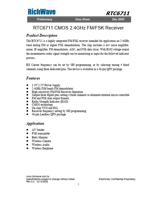
R8C/2A Group, R8C/2B GroupRENESAS MCU1.Overview1.1FeaturesThe R8C/2A Group and R8C/2B Group of single-chip MCUs incorporates the R8C/Tiny Series CPU core,employing sophisticated instructions for a high level of efficiency. With 1 Mbyte of address space and is capable of executing instructions at high speed. In addition, the CPU core boasts a multiplier for high-speed operation processing.Power consumption is low, and the supported operating modes allow additional power control. These MCUs also use an anti-noise configuration to reduce emissions of electromagnetic noise and are designed to withstand EMI.Integration of many peripheral functions, including multifunction timer and serial interface, reduces the number of system components.Furthermore, the R8C/2B Group has on-chip data flash (1 KB × 2 blocks).The difference between the R8C/2A Group and R8C/2B Group is only the presence or absence of data flash. Their peripheral functions are the same.1.1.1ApplicationsElectronic household appliances, office equipment, audio equipment, consumer equipment, etc.REJ03B0182-0100Rev.1.00Feb 09, 20071.1.2SpecificationsTables 1.1 and 1.2 outlines the Specifications for R8C/2A Group and Tables 1.3 and 1.4 outlines the Specifications for R8C/2B GroupTable 1.1Specifications for R8C/2A Group (1)Item Function SpecificationCPU Central processingunit R8C/Tiny series core•Number of fundamental instructions: 89•Minimum instruction execution time:50 ns (f(XIN) = 20 MHz, VCC = 3.0 to 5.5 V)100 ns (f(XIN) = 10 MHz, VCC = 2.7 to 5.5 V)200 ns (f(XIN) = 5 MHz, VCC = 2.2 to 5.5 V)•Multiplier: 16 bits × 16 bits → 32 bits•Multiply-accumulate instruction: 16 bits × 16 bits + 32 bits → 32 bits •Operation mode: Single-chip mode (address space: 1 Mbyte)Memory ROM, RAM Refer to Table 1.5 Product List for R8C/2A Group.Power Supply Voltage Detection Voltage detectioncircuit•Power-on reset•Voltage detection 2I/O Ports Programmable I/Oports •Input-only: 2 pins•CMOS I/O ports: 55, selectable pull-up resistor •High current drive ports: 8Clock Clock generationcircuits 3 circuits: XIN clock oscillation circuit (with on-chip feedback resistor),On-chip oscillator (high-speed, low-speed)(high-speed on-chip oscillator has a frequency adjustment function),XCIN clock oscillation circuit (32 kHz)•Oscillation stop detection: XIN clock oscillation stop detection function •Frequency divider circuit: Dividing selectable 1, 2, 4, 8, and 16•Low power consumption modes:Standard operating mode (high-speed clock, low-speed clock, high-speed on-chip oscillator, low-speed on-chip oscillator), wait mode, stop modeInterrupts•External: 5 sources, Internal: 23 sources, Software: 4 sources•Priority levels: 7 levelsWatchdog Timer15 bits × 1 (with prescaler), reset start selectableTimer Timer RA8 bits × 1 (with 8-bit prescaler)Timer mode (period timer), pulse output mode (output level inverted everyperiod), event counter mode, pulse width measurement mode, pulse periodmeasurement modeTimer RB8 bits × 1 (with 8-bit prescaler)Timer mode (period timer), programmable waveform generation mode (PWMoutput), programmable one-shot generation mode, programmable wait one-shot generation modeTimer RC16 bits × 1 (with 4 capture/compare registers)Timer mode (input capture function, output compare function), PWM mode(output 3 pins), PWM2 mode (PWM output pin)Timer RD16 bits × 2 (with 4 capture/compare registers)Timer mode (input capture function, output compare function), PWM mode(output 6 pins), reset synchronous PWM mode (output three-phasewaveforms (6 pins), sawtooth wave modulation), complementary PWM mode(output three-phase waveforms (6 pins), triangular wave modulation), PWM3mode (PWM output 2 pins with fixed period)Timer RE8 bits × 1Real-time clock mode (count seconds, minutes, hours, days of week), outputcompare modeTimer RF16 bits × 1 (with capture/compare register pin and compare register pin)Input capture mode, output compare modeNOTES:1.I 2C bus is a trademark of Koninklijke Philips Electronics N. V.2.Specify the D version if D version functions are to be used.Table 1.2Specifications for R8C/2A Group (2)Item Function SpecificationSerial Interface UART0, UART1, UART2Clock synchronous serial I/O/UART × 3Clock Synchronous Serial I/O with Chip Select (SSU) 1 (shared with I 2C-bus)I 2C bus (1) 1 (shared with SSU)LIN Module Hardware LIN: 1 (timer RA, UART0)A/D Converter 10-bit resolution × 12 channels, includes sample and hold function D/A Converter 8-bit resolution × 2 circuitsFlash Memory•Programming and erasure voltage: VCC = 2.7 to 5.5 V •Programming and erasure endurance: 100 times •Program security: ROM code protect, ID code check•Debug functions: On-chip debug, on-board flash rewrite function Operating Frequency/Supply Voltagef(XIN) = 20 MHz (VCC = 3.0 to 5.5 V)f(XIN) = 10 MHz (VCC = 2.7 to 5.5 V)f(XIN) = 5 MHz (VCC = 2.2 to 5.5 V)Current consumption12 mA (VCC = 5.0 V, f(XIN) = 20 MHz)5.5 mA (VCC = 3.0 V, f(XIN) = 10 MHz)2.1 µA (VCC =3.0 V, wait mode (f(XCIN) = 32 kHz))0.65 µA (VCC = 3.0 V, stop mode)Operating Ambient Temperature -20 to 85°C (N version)-40 to 85°C (D version)(2)Package64-pin LQFP•Package code: PLQP0064KB-A (previous code: 64P6Q-A)•Package code: PLQP0064GA-A (previous code: 64P6U-A)Table 1.3Specifications for R8C/2B Group (1)Item Function SpecificationCPU Central processingunit R8C/Tiny series core•Number of fundamental instructions: 89•Minimum instruction execution time:50 ns (f(XIN) = 20 MHz, VCC = 3.0 to 5.5 V)100 ns (f(XIN) = 10 MHz, VCC = 2.7 to 5.5 V)200 ns (f(XIN) = 5 MHz, VCC = 2.2 to 5.5 V)•Multiplier: 16 bits × 16 bits → 32 bits•Multiply-accumulate instruction: 16 bits × 16 bits + 32 bits → 32 bits •Operation mode: Single-chip mode (address space: 1 Mbyte)Memory ROM, RAM Refer to Table 1.6 Product List for R8C/2B Group.Power Supply Voltage Detection Voltage detectioncircuit•Power-on reset•Voltage detection 2I/O Ports Programmable I/Oports •Input-only: 2 pins•CMOS I/O ports: 55, selectable pull-up resistor •High current drive ports: 8Clock Clock generationcircuits 3 circuits: XIN clock oscillation circuit (with on-chip feedback resistor),On-chip oscillator (high-speed, low-speed)(high-speed on-chip oscillator has a frequency adjustment function),XCIN clock oscillation circuit (32 kHz)•Oscillation stop detection: XIN clock oscillation stop detection function •Frequency divider circuit: Dividing selectable 1, 2, 4, 8, and 16•Low power consumption modes:Standard operating mode (high-speed clock, low-speed clock, high-speed on-chip oscillator, low-speed on-chip oscillator), wait mode, stop modeInterrupts•External: 5 sources, Internal: 23 sources, Software: 4 sources•Priority levels: 7 levelsWatchdog Timer15 bits × 1 (with prescaler), reset start selectableTimer Timer RA8 bits × 1 (with 8-bit prescaler)Timer mode (period timer), pulse output mode (output level inverted everyperiod), event counter mode, pulse width measurement mode, pulse periodmeasurement modeTimer RB8 bits × 1 (with 8-bit prescaler)Timer mode (period timer), programmable waveform generation mode (PWMoutput), programmable one-shot generation mode, programmable wait one-shot generation modeTimer RC16 bits × 1 (with 4 capture/compare registers)Timer mode (input capture function, output compare function), PWM mode(output 3 pins), PWM2 mode (PWM output pin)Timer RD16 bits × 2 (with 4 capture/compare registers)Timer mode (input capture function, output compare function), PWM mode(output 6 pins), reset synchronous PWM mode (output three-phasewaveforms (6 pins), sawtooth wave modulation), complementary PWM mode(output three-phase waveforms (6 pins), triangular wave modulation), PWM3mode (PWM output 2 pins with fixed period)Timer RE8 bits × 1Real-time clock mode (count seconds, minutes, hours, days of week), outputcompare modeTimer RF16 bits × 1 (with capture/compare register pin and compare register pin)Input capture mode, output compare modeNOTES:1.I 2C bus is a trademark of Koninklijke Philips Electronics N. V.2.Specify the D version if D version functions are to be used.Table 1.4Specifications for R8C/2B Group (2)Item Function SpecificationSerial Interface UART0, UART1, UART2Clock synchronous serial I/O/UART × 3Clock Synchronous Serial I/O with Chip Select (SSU) 1 (shared with I 2C-bus)I 2C bus (1) 1 (shared with SSU)LIN Module Hardware LIN: 1 (timer RA, UART0)A/D Converter 10-bit resolution × 12 channels, includes sample and hold function D/A Converter 8-bit resolution × 2 circuitsFlash Memory•Programming and erasure voltage: VCC = 2.7 to 5.5 V•Programming and erasure endurance: 10,000 times (data flash)1,000 times (program ROM)•Program security: ROM code protect, ID code check•Debug functions: On-chip debug, on-board flash rewrite function Operating Frequency/Supply Voltagef(XIN) = 20 MHz (VCC = 3.0 to 5.5 V)f(XIN) = 10 MHz (VCC = 2.7 to 5.5 V)f(XIN) = 5 MHz (VCC = 2.2 to 5.5 V)Current consumption12 mA (VCC = 5.0 V, f(XIN) = 20 MHz)5.5 mA (VCC = 3.0 V, f(XIN) = 10 MHz)2.1 µA (VCC =3.0 V, wait mode (f(XCIN) = 32 kHz))0.65 µA (VCC = 3.0 V, stop mode)Operating Ambient Temperature -20 to 85°C (N version)-40 to 85°C (D version)(2)Package64-pin LQFP•Package code: PLQP0064KB-A (previous code: 64P6Q-A)•Package code: PLQP0064GA-A (previous code: 64P6U-A)1.2Product ListTable 1.5 lists Product List for R8C/2A Group, Figure 1.1 shows a Part Number, Memory Size, and Package of R8C/2A Group, Table 1.6 lists Product List for R8C/2B Group, and Figure 1.2 shows a Part Number, Memory Size, and Package of R8C/2B Group.Table 1.5Product List for R8C/2A Group Current of Feb. 2007 Part No.ROM Capacity RAM Capacity Package Type RemarksR5F212A7SNFP48 Kbytes 2.5 Kbytes PLQP0064KB-A N versionR5F212A7SNFA48 Kbytes 2.5 Kbytes PLQP0064GA-AR5F212A8SNFP64 Kbytes 3 Kbytes PLQP0064KB-AR5F212A8SNFA64 Kbytes 3 Kbytes PLQP0064GA-AR5F212AASNFP (D)96 Kbytes7 Kbytes PLQP0064KB-AR5F212AASNFA (D)96 Kbytes7 Kbytes PLQP0064GA-AR5F212ACSNFP (D)128 Kbytes7.5 Kbytes PLQP0064KB-AR5F212ACSNFA (D)128 Kbytes7.5 Kbytes PLQP0064GA-AR5F212A7SDFP (D)48 Kbytes 2.5 Kbytes PLQP0064KB-A D versionR5F212A7SDFA (D)48 Kbytes 2.5 Kbytes PLQP0064GA-AR5F212A8SDFP (D)64 Kbytes 3 Kbytes PLQP0064KB-AR5F212A8SDFA (D)64 Kbytes 3 Kbytes PLQP0064GA-AR5F212AASDFP (D)96 Kbytes7 Kbytes PLQP0064KB-AR5F212AASDFA (D)96 Kbytes7 Kbytes PLQP0064GA-AR5F212ACSDFP (D)128 Kbytes7.5 Kbytes PLQP0064KB-AR5F212ACSDFA (D)128 Kbytes7.5 Kbytes PLQP0064GA-A(D): Under development(D): Under developmentTable 1.6Product List for R8C/2B GroupCurrent of Feb. 2007Part No.ROM CapacityRAMCapacity Package TypeRemarksProgram ROM Data flash R5F212B7SNFP 48 Kbytes 1 Kbyte × 2 2.5 Kbytes PLQP0064KB-A N version R5F212B7SNFA 48 Kbytes 1 Kbyte × 2 2.5 Kbytes PLQP0064GA-A R5F212B8SNFP 64 Kbytes 1 Kbyte × 2 3 Kbytes PLQP0064KB-A R5F212B8SNFA 64 Kbytes 1 Kbyte × 2 3 Kbytes PLQP0064GA-A R5F212BASNFP (D)96 Kbytes 1 Kbyte × 27 Kbytes PLQP0064KB-A R5F212BASNFA (D)96 Kbytes 1 Kbyte × 27 Kbytes PLQP0064GA-A R5F212BCSNFP (D)128 Kbytes 1 Kbyte × 27.5 Kbytes PLQP0064KB-A R5F212BCSNFA (D)128 Kbytes 1 Kbyte × 27.5 Kbytes PLQP0064GA-AR5F212B7SDFP (D)48 Kbytes 1 Kbyte × 2 2.5 Kbytes PLQP0064KB-A D version R5F212B7SDFA (D)48 Kbytes 1 Kbyte × 2 2.5 Kbytes PLQP0064GA-A R5F212B8SDFP (D)64 Kbytes 1 Kbyte × 2 3 Kbytes PLQP0064KB-A R5F212B8SDFA (D)64 Kbytes 1 Kbyte × 2 3 Kbytes PLQP0064GA-A R5F212BASDFP (D)96 Kbytes 1 Kbyte × 27 Kbytes PLQP0064KB-A R5F212BASDFA (D)96 Kbytes 1 Kbyte × 27 Kbytes PLQP0064GA-A R5F212BCSDFP (D)128 Kbytes 1 Kbyte × 27.5 Kbytes PLQP0064KB-A R5F212BCSDFA (D)128 Kbytes 1 Kbyte × 27.5 KbytesPLQP0064GA-A1.3 Block DiagramFigure 1.3 shows a Block Diagram.1.4Pin AssignmentFigure 1.4 shows Pin Assignment (Top View). Tables 1.7 and 1.8 outlines the Pin Name Information by Pin Number.NOTE:1.Can be assigned to the pin in parentheses by a program.Table 1.7Pin Name Information by Pin Number (1)PinNumber Control PinPort I/O Pin Functions for of Peripheral ModulesInterruptTimer SerialInterfaceSSU I 2C busA/D Converter,D/A Converter1P3_3SSI 2P3_4SCS SDA3MODE 4XCIN P4_35XCOUT P4_46RESET 7XOUT P4_78VSS/AVSS9XIN P4_610VCC/AVCC11P5_4TRCIOD 12P5_3TRCIOC 13P5_2TRCIOB14P5_1TRCIOA/TRCTRG15P5_0TRCCLK 16P2_7TRDIOD117P2_6TRDIOC118P2_5TRDIOB119P2_4TRDIOA120P2_3TRDIOD021P2_2TRDIOC022P2_1TRDIOB023P2_0TRDIOA0/TRDCLK24P1_7INT1TRAIO25P1_6CLK026P1_5(INT1)(1)(TRAIO)(1)RXD027P1_4TXD028P8_629P8_5TRFO1230P8_4TRFO1131P8_3TRFO10/TRFI 32P8_2TRFO0233P8_1TRFO0134P8_0TRFO0035P6_0TREO 36P4_5INT0INT037P6_6INT2TXD138P6_7INT3RXD139P6_5(CLK1)(1)/CLK240P6_4RXD241P6_3TXD242P3_1TRBO 43P3_0TRAO44P3_6(INT1)(1)45P3_2(INT2)(1)Table 1.8Pin Name Information by Pin Number (2)Pin Number Control Pin PortI/O Pin Functions for of Peripheral ModulesInterrupt TimerSerialInterfaceSSU I2C busA/D Converter,D/A Converter46P1_3Kl3AN11 47P1_2KI2AN10 48P1_1KI1AN9 49P1_0KI0AN8 50P0_0AN7 51P0_1AN6 52P0_2AN5 53P0_3AN4 54P0_4AN3 55P6_256P6_157P0_5CLK1AN2 58P0_6AN1/DA0 59VSS/AVSS60P0_7AN0/DA1 61VREF62VCC/AVCC63P3_7SSO64P3_5SSCK SCL1.5Pin FunctionsTables 1.9 and 1.10 list Pin Functions.I: Input O: Output I/O: Input and output NOTE:1.Refer to the oscillator manufacturer for oscillation characteristics.Table 1.9Pin Functions (1)ItemPin Name I/O TypeDescriptionPower supply input VCC, VSS −Apply 2.2 V to 5.5 V to the VCC pin. Apply 0 V to the VSS pin.Analog power supply input AVCC, AVSS −Power supply for the A/D converter.Connect a capacitor between AVCC and AVSS.Reset input RESET I Input “L” on this pin resets the MCU.MODE MODE I Connect this pin to VCC via a resistor.XIN clock input XIN I These pins are provided for XIN clock generation circuit I/O.Connect a ceramic resonator or a crystal oscillator between the XIN and XOUT pins (1). To use an external clock, input it to the XIN pin and leave the XOUT pin open.XIN clock output XOUT O XCIN clock input XCIN I These pins are provided for XCIN clock generation circuit I/O.Connect a crystal oscillator between the XCIN and XCOUT pins (1). To use an external clock, input it to the XCIN pin and leave the XCOUT pin open.XCIN clock output XCOUT O INT interrupt input INT0 to INT3I INT interrupt input pins.INT0 is timer RD input pin. INT1 is timer RA input pin.Key input interrupt KI0 to KI3I Key input interrupt input pins Timer RA TRAIO I/O Timer RA I/O pin TRAO O Timer RA output pin Timer RB TRBO O Timer RB output pin Timer RCTRCCLK I External clock input pin TRCTRGI External trigger input pin TRCIOA, TRCIOB,TRCIOC, TRCIODI/O Timer RC I/O pins Timer RDTRDIOA0, TRDIOA1, TRDIOB0, TRDIOB1, TRDIOC0, TRDIOC1, TRDIOD0, TRDIOD1I/OTimer RD I/O pinsTRDCLK I External clock input pin Timer RE TREO O Divided clock output pin Timer RFTRFII Timer RF input pin TRFO00 to TRFO02, TRFO10 to TRFO12O Timer RF output pins Serial interface CLK0, CLK1, CLK2I/O Transfer clock I/O pins RXD0, RXD1, RXD2I Serial data input pins TXD0, TXD1, TXD2O Serial data output pins I 2C bus SCL I/O Clock I/O pin SDA I/O Data I/O pin SSUSSI I/O Data I/O pinSCS I/O Chip-select signal I/O pin SSCK I/O Clock I/O pin SSOI/O Data I/O pinReference voltage inputVREFIReference voltage input pin to A/D converter and D/A converterTable 1.10Pin Functions (2)Item Pin Name I/O Type Description A/D converter AN0 to AN11I Analog input pins to A/D converter D/A converter DA0 to DA1O D/A converter output pinsI/O port P0_0 to P0_7,P1_0 to P1_7,P2_0 to P2_7,P3_0 to P3_7,P4_3 to P4_5,P5_0 to P5_4,P6_0 to P6_7,P8_0 to P8_6I/O CMOS I/O ports. Each port has an I/O select direction register, allowing each pin in the port to be directed for inputor output individually.Any port set to input can be set to use a pull-up resistor or notby a program.P2_0 to P2_7 also function as LED drive ports.Input port P4_6, P4_7I Input-only portsI: Input O: Output I/O: Input and output2.Central Processing Unit (CPU)Figure 2.1 shows the CPU Registers. The CPU contains 13 registers. R0, R1, R2, R3, A0, A1, and FB configure a register bank. There are two sets of register bank.2.1Data Registers (R0, R1, R2, and R3)R0 is a 16-bit register for transfer, arithmetic, and logic operations. The same applies to R1 to R3. R0 can be split into high-order bits (R0H) and low-order bits (R0L) to be used separately as 8-bit data registers. R1H and R1L are analogous to R0H and R0L. R2 can be combined with R0 and used as a 32-bit data register (R2R0). R3R1 is analogous to R2R0.2.2Address Registers (A0 and A1)A0 is a 16-bit register for address register indirect addressing and address register relative addressing. It is also used for transfer, arithmetic, and logic operations. A1 is analogous to A0. A1 can be combined with A0 and as a 32-bit address register (A1A0).2.3Frame Base Register (FB)FB is a 16-bit register for FB relative addressing.2.4Interrupt Table Register (INTB)INTB is a 20-bit register that indicates the start address of an interrupt vector table.2.5Program Counter (PC)PC is 20 bits wide and indicates the address of the next instruction to be executed.2.6User Stack Pointer (USP) and Interrupt Stack Pointer (ISP)The stack pointers (SP), USP, and ISP, are each 16 bits wide. The U flag of FLG is used to switch betweenUSP and ISP.2.7Static Base Register (SB)SB is a 16-bit register for SB relative addressing.2.8Flag Register (FLG)FLG is an 11-bit register indicating the CPU state.2.8.1Carry Flag (C)The C flag retains carry, borrow, or shift-out bits that have been generated by the arithmetic and logic unit.2.8.2Debug Flag (D)The D flag is for debugging only. Set it to 0.2.8.3Zero Flag (Z)The Z flag is set to 1 when an arithmetic operation results in 0; otherwise to 0.2.8.4Sign Flag (S)The S flag is set to 1 when an arithmetic operation results in a negative value; otherwise to 0.2.8.5Register Bank Select Flag (B)Register bank 0 is selected when the B flag is 0. Register bank 1 is selected when this flag is set to 1.2.8.6Overflow Flag (O)The O flag is set to 1 when an operation results in an overflow; otherwise to 0.2.8.7Interrupt Enable Flag (I)The I flag enables maskable interrupts.Interrupt are disabled when the I flag is set to 0, and are enabled when the I flag is set to 1. The I flag is set to 0 when an interrupt request is acknowledged.2.8.8Stack Pointer Select Flag (U)ISP is selected when the U flag is set to 0; USP is selected when the U flag is set to 1.The U flag is set to 0 when a hardware interrupt request is acknowledged or the INT instruction of software interrupt numbers 0 to 31 is executed.2.8.9Processor Interrupt Priority Level (IPL)IPL is 3 bits wide and assigns processor interrupt priority levels from level 0 to level 7.If a requested interrupt has higher priority than IPL, the interrupt is enabled.2.8.10Reserved BitIf necessary, set to 0. When read, the content is undefined.3.Memory3.1R8C/2A GroupFigure 3.1 is a Memory Map of R8C/2A Group. The R8C/2A group has 1 Mbyte of address space from addresses 00000h to FFFFFh.The internal ROM is allocated lower addresses, beginning with address 0FFFFh. For example, a 48-Kbyte internal ROM area is allocated addresses 04000h to 0FFFFh.The fixed interrupt vector table is allocated addresses 0FFDCh to 0FFFFh. They store the starting address of each interrupt routine.The internal RAM is allocated higher addresses, beginning with address 00400h. For example, a 2.5-Kbyte internal RAM area is allocated addresses 00400h to 00DFFh. The internal RAM is used not only for storing data but also for calling subroutines and as stacks when interrupt requests are acknowledged.Special function registers (SFRs) are allocated addresses 00000h to 002FFh. The peripheral function control registers are allocated here. All addresses within the SFR, which have nothing allocated are reserved for future use and cannot be accessed by users.3.2R8C/2B GroupFigure 3.2 is a Memory Map of R8C/2B Group. The R8C/2B group has 1 Mbyte of address space from addresses 00000h to FFFFFh.The internal ROM (program ROM) is allocated lower addresses, beginning with address 0FFFFh. For example, a 48-Kbyte internal ROM area is allocated addresses 04000h to 0FFFFh.The fixed interrupt vector table is allocated addresses 0FFDCh to 0FFFFh. They store the starting address of each interrupt routine.The internal ROM (data flash) is allocated addresses 02400h to 02BFFh.The internal RAM area is allocated higher addresses, beginning with address 00400h. For example, a 2.5-Kbyte internal RAM is allocated addresses 00400h to 00DFFh. The internal RAM is used not only for storing data but also for calling subroutines and as stacks when interrupt requests are acknowledged.Special function registers (SFRs) are allocated addresses 00000h to 002FFh. The peripheral function control registers are allocated here. All addresses within the SFR, which have nothing allocated are reserved for future use and cannot be accessed by users.4.Special Function Registers (SFRs)An SFR (special function register) is a control register for a peripheral function. Tables 4.1 to 4.12 list the special function registers.Table 4.1SFR Information (1)(1)Address Register Symbol After reset0000h0001h0002h0003h0004h Processor Mode Register 0PM000h0005h Processor Mode Register 1PM100h0006h System Clock Control Register 0CM001101000b0007h System Clock Control Register 1CM100100000b0008h Module Operation Enable Register MSTCR00h0009h000Ah Protect Register PRCR00h000Bh000Ch Oscillation Stop Detection Register OCD00000100b000Dh Watchdog Timer Reset Register WDTR XXh000Eh Watchdog Timer Start Register WDTS XXh000Fh Watchdog Timer Control Register WDC00X11111b0010h Address Match Interrupt Register 0RMAD000h0011h00h0012h00h0013h Address Match Interrupt Enable Register AIER00h0014h Address Match Interrupt Register 1RMAD100h0015h00h0016h00h0017h0018h0019h001Ah001Bh001Ch Count Source Protection Mode Register CSPR00h10000000b(6) 001Dh001Eh001Fh0020h0021h0022h0023h High-Speed On-Chip Oscillator Control Register 0FRA000h0024h High-Speed On-Chip Oscillator Control Register 1FRA1When shipping0025h High-Speed On-Chip Oscillator Control Register 2FRA200h0026h0027h0028h Clock Prescaler Reset Flag CPSRF00h0029h002Ah002Bh High-Speed On-Chip Oscillator Control Register 6FRA6When Shipping0030h0031h Voltage Detection Register 1(2)VCA100001000b0032h Voltage Detection Register 2(2)VCA200h(3)00100000b(4) 0033h0034h0035h0036h Voltage Monitor 1 Circuit Control Register(5)VW1C00001000b0037h Voltage Monitor 2 Circuit Control Register(5)VW2C00h0038h Voltage Monitor 0 Circuit Control Register(2)VW0C0000X000b(3)0100X001b(4) 0039h003Ah003Bh003Ch003Dh003Eh003FhX: UndefinedNOTES:1.The blank regions are reserved. Do not access locations in these regions.2.Software reset, watchdog timer reset, voltage monitor 1 reset, or voltage monitor 2 reset do not affect this register.3.The LVD0ON bit in the OFS register is set to 1 and hardware reset.4.Power-on reset, voltage monitor 0 reset, or the LVD0ON bit in the OFS register is set to 0 and hardware reset.5.Software reset, watchdog timer reset, voltage monitor 1 reset, or voltage monitor 2 reset do not affect b2 and b3.6.The CSPROINI bit in the OFS register is set to 0.Table 4.2SFR Information (2)(1)Address Register Symbol After reset 0040h0041h0042h0043h0044h0045h0046h0047h Timer RC Interrupt Control Register TRCIC XXXXX000b 0048h Timer RD0 Interrupt Control Register TRD0IC XXXXX000b 0049h Timer RD1 Interrupt Control Register TRD1IC XXXXX000b 004Ah Timer RE Interrupt Control Register TREIC XXXXX000b 004Bh UART2 Transmit Interrupt Control Register S2TIC XXXXX000b 004Ch UART2 Receive Interrupt Control Register S2RIC XXXXX000b 004Dh Key Input Interrupt Control Register KUPIC XXXXX000b 004Eh004Fh SSU/IIC Interrupt Control Register(2)SSUIC / IICIC XXXXX000b 0050h Compare 1 Interrupt Control Register CMP1IC XXXXX000b 0051h UART0 Transmit Interrupt Control Register S0TIC XXXXX000b 0052h UART0 Receive Interrupt Control Register S0RIC XXXXX000b 0053h UART1 Transmit Interrupt Control Register S1TIC XXXXX000b 0054h UART1 Receive Interrupt Control Register S1RIC XXXXX000b 0055h INT2 Interrupt Control Register INT2IC XX00X000b 0056h Timer RA Interrupt Control Register TRAIC XXXXX000b 0057h0058h Timer RB Interrupt Control Register TRBIC XXXXX000b 0059h INT1 Interrupt Control Register INT1IC XX00X000b 005Ah INT3 Interrupt Control Register INT3IC XX00X000b 005Bh Timer RF Interrupt Control Register TRFIC XXXXX000b 005Ch Compare 0 Interrupt Control Register CMP0IC XXXXX000b 005Dh INT0 Interrupt Control Register INT0IC XX00X000b 005Eh A/D Conversion Interrupt Control Register ADIC XXXXX000b 005Fh Capture Interrupt Control Register CAPIC XXXXX000b 0060h0061h0062h0063h0064h0065h0066h0067h0068h0069h006Ah006Bh006Ch006Dh006Eh006Fh0070h0071h0072h0073h0074h0075h0076h0077h0078h0079h007Ah007Bh007Ch007Dh007Eh007FhX: UndefinedNOTES:1.The blank regions are reserved. Do not access locations in these regions.2.Selected by the IICSEL bit in the PMR register.Table 4.3SFR Information (3)(1)Address Register Symbol After reset 0080h0081h0082h0083h0084h0085h0086h0087h0088h0089h008Ah008Bh008Ch008Dh008Eh008Fh0090h0091h0092h0093h0094h0095h0096h0097h0098h0099h009Ah009Bh009Ch009Dh009Eh009Fh00A0h UART0 Transmit/Receive Mode Register U0MR00h00A1h UART0 Bit Rate Register U0BRG XXh00A2h UART0 Transmit Buffer Register U0TB XXh00A3h XXh00A4h UART0 Transmit/Receive Control Register 0U0C000001000b 00A5h UART0 Transmit/Receive Control Register 1U0C100000010b 00A6h UART0 Receive Buffer Register U0RB XXh00A7h XXh00A8h UART1 Transmit/Receive Mode Register U1MR00h00A9h UART1 Bit Rate Register U1BRG XXh00AAh UART1 Transmit Buffer Register U1TB XXh00ABh XXh00ACh UART1 Transmit/Receive Control Register 0U1C000001000b 00ADh UART1 Transmit/Receive Control Register 1U1C100000010b 00AEh UART1 Receive Buffer Register U1RB XXh00AFh XXh00B0h00B1h00B2h00B3h00B4h00B5h00B6h00B7h00B8h SS Control Register H / IIC bus Control Register 1(2)SSCRH / ICCR100h00B9h SS Control Register L / IIC bus Control Register 2(2)SSCRL / ICCR201111101b 00BAh SS Mode Register / IIC bus Mode Register(2)SSMR / ICMR00011000b 00BBh SS Enable Register / IIC bus Interrupt Enable Register(2)SSER / ICIER00h00BCh SS Status Register / IIC bus Status Register(2)SSSR / ICSR00h / 0000X000b 00BDh SS Mode Register 2 / Slave Address Register(2)SSMR2 / SAR00h00BEh SS Transmit Data Register / IIC bus Transmit Data Register(2)SSTDR / ICDRT FFh00BFh SS Receive Data Register / IIC bus Receive Data Register(2)SSRDR / ICDRR FFhX: UndefinedNOTES:1.The blank regions are reserved. Do not access locations in these regions.2.Selected by the IICSEL bit in the PMR register.。
自积分型CMOS读出电路硅光二极管阵列的性能分析
第7卷第15期2007年8月 1671—1819(2007)15—3694—04
科学技术与工程
Science Technology and Engineering Vo1.7 No.15 Aug.2007
⑥2007 Sci.Tech.Engng.
自积分型CMOS读出电路硅光二极管 阵列的性能分析
陈世军张学敏 (中国科学院上海技术物理研究所,上海200083)
摘要给出了自积分型(sI)读出电路(ROIC)构成的光电二极管阵列的电路结构,对该电路的工作原理进行了分析,讨论 了电路工作时的电荷转移过程、传输效率、噪声等特性。该读出电路结构简单,适合大规模焦平面阵列。针对电路的具体性 能参数测试,还进行了理论分析、推导和计算,最后提供了样品的测试参数。 关键词 自积分读出电路 光电二极管阵列 CMOS移位寄存器 中图法分类号TN43; 文献标识码A
介绍了我们研制的集成光电探测器阵列。它 与传统的半导体光敏器件相比,最为明显的特点是 将硅光电二极管阵列、信号读出电路(ROIC)及输出 电路集成在一个芯片上,使得整个系统的可靠性明 显提高,噪声也大幅度减小。 SI自积分型读出电路结构由于结构简单,因而 在要求高密度、大面积和低功耗的电路中,广泛地 应用。用硅光二极管阵列与SI型MOSFET开关读 出电路构成的光电探测器阵列是一种基本、重要, 而且常用的结构形式,具有较强的代表性和普遍 性。它具有分辨率高、抗辐射性能强、光敏元形状 及尺寸设计灵活、外围电路简单等优点…。它的研 究对直接注入型、缓冲直接注入型、源跟随型等的 读出电路构成的光电探测器阵列有着重要的意义。 1电路结构及工作原理 1.1电路结构 图1为电路结构图。、每个单元都有一个有效光 电二极管、一个哑元二极管和一个相应的CMOS开 关多路传输器组成,其信号读出采用自积分模式 2007年5月1日收到 第一作者简介:陈世军(1967一),女,上海人,研究方向:半导体 器件测试及集成电路设计。E—mail:susan1967@cifiz.net。 工作。
MEMS 教程 Lecture16
Final Exam details
50% multiple choice. 50% free response. All multiple choice material come from previous quizzes Questions will be worded slightly differently than on quizzes Questions will focus on understanding concepts and applications, not rote memorization Exception: You must know certain “famous” MEMS devices by name (e.g. Texas Instruments DMD, Analog Devices ADXL 50). Free response questions will require you to sketch drawings Know Know Know Know how basic devices look how basic devices work basic sizes and materials how fabrication processes work
Introduction to MEMS Final Review A review of some of the many issues discussed in this class
Introduction to MEMS lecture #16 FINAL LECTURE Mark Bachman, UCI, Fall 2004
16
Diffuser valve devices
You should know: Basic design, materials, operation, application, fabrication
KAC-9648;中文规格书,Datasheet资料
PRODUCT SUMMARYKODAK KAC-9648 IMAGE SENSOR1288 (H) X 1032 (V) COLOR CMOS IMAGE SENSOR DESCRIPTIONThe KODAK KAC-9648 Image Sensor is a high performance, low power, 1/2" SXGA CMOS Active Pixel Sensor capable of capturing color, monochrome, still, or motion images and converting them to a digital data stream.Mega-pixel class image quality is achieved by integrating a high performance analog signal processor comprising of a high speed 10 bit A/D converter, fixed pattern noise elimination circuits and separate color gain amplifiers. The offset and black level can be automatically adjusted on chip using a full loop black level compensation circuit. Furthermore, a programmable smart timing and control circuit allows the user maximum flexibility in adjusting integration time, active window size, gain, frame rate. Various control, timing and power modes are also provided.FEATURES• Video and snapshot operation• Progressive scan read out with horizontal and vertical flip• Programmable exposure with master clock divider, inter row delay, inter frame delay, andpartial frame integration• Four channels of digitally programmable analog gain• Full automatic servo loop for black level & offset adjustment on each gain channel• Horizontal & vertical sub-sampling (2:1 & 4:2) with averaging• Windowing• Programmable pixel clock, inter-frame and inter-line delays• I2C compatible serial control interface Parameter TypicalValue Array Format Total: 1032 x 1312Active: 1032 (V) x 1288 (H)Effective Image Area Total: 6.192mm x 7.872mmActive: 6.192mm x 7.728mmOptical Format 1/2"Pixel Size 6.0 µm x 6.0 µmVideo Outputs 8 & 10 Bit DigitalFrame Rate 18 frames per secondDynamic Range 55 dBShutter Rollingreset FPN 0.2% PRNU 1.7% Sensitivity 2.5V/lux*sFill Factor 49%Color Mosaic Bayer patternMicrolens none Package 48LCC Single Supply 3.0V ± 10%Power Consumption 150mWOperating Temp -10° C to 50° CAPPLICATIONS• Dual Mode Camera• Digital Still Camera• Security Camera• Machine Vision/go/imagersCHIP BLOCK DIAGRAMORDERING INFORMATIONProduct Name DescriptionCatalogNumber4H0723 KAC- 9648-CBA-FB-AA Color (Bayer RGB), Telecentric Microlens, CLCC Package, Clear Cover Glass (no coatings), Standard Grade 3F5386 KEM-3F5386-KAC-96XX Evaluation Board (Main Board)3F5385 KEH-3F5385-KAC-9648 Evaluation Board (Head Board)Please see ISS Application Note “Product Naming Convention” (MTD/PS-0892) for a full description of naming convention used for KODAK image sensors.Address all inquiries and purchase orders to:Image Sensor SolutionsEastman Kodak CompanyRochester, New York 14650-2010Phone: (585) 722-4385Fax: (585) 477-4947E-mail: imagers@©Eastman Kodak Company, 2006. Kodak and Pixelux are trademarks. Revision 2.0分销商库存信息: KODAKKAC-9648。
RTC6705
Confidential Proprietary
Free Datasheet
RTC6705-DST-001
Block Diagram
Data Sheet
RTC6705
SEP 2007
L DO 2V5 VCOVDD GND NC NC PAO UT 1 PAOUT2 R FG ND PAVDD BUFVDD
Power consumption for reference design with 2dBm output power
Power consumption for chip with 13dBm output power Oscillator operating frequency
SPI_SE NC S BX
SPIDATA/CS0 SPILE/CS1
SPICLK/CS2 VDD33_DIG V2D5_PLL VT_Mod
10
9
8
7
6
5
4
3
2
1
40
39
38
37
36
35
34
33
32
31
5 GHz N/A Counter
SPI/REGIST ER_CONT
PA1
PA2 5GHz_PA
3.3V Analog power supply for VCO
Specifications subject to change without notice V0.2
3
Confidential Proprietary
Free Datasheet
ELECTRICAL SPECIFICATIONS
(1) Absolute Maximum Ratings
- 1、下载文档前请自行甄别文档内容的完整性,平台不提供额外的编辑、内容补充、找答案等附加服务。
- 2、"仅部分预览"的文档,不可在线预览部分如存在完整性等问题,可反馈申请退款(可完整预览的文档不适用该条件!)。
- 3、如文档侵犯您的权益,请联系客服反馈,我们会尽快为您处理(人工客服工作时间:9:00-18:30)。
A 0.8V 64x64 CMOS Imager with Integrated Sense-and-Stimulus Pixel for Artificial Retina ApplicationsChih-Lin Lee and Chih-Cheng HsiehSignal Sensing and Application LaboratoryDepartment of Electrical Engineering, National Tsing Hua UniversityHsinchu, Taiwan, R.O.CEmail: g9761571@.twAbstract —A 0.8V 64x64 CMOS Image Sensor (CIS) array with integrated sense-and-stimulus (SAS) pixel is presented in this paper. The in-pixel photon-to-biphasic-current converter (sense) and balanced current-mode stimulator (stimulus) are proposed to achieve a high integration and low power solution for high-resolution vision recovery. Two operation modes as programming (PG) mode and implanted (IP) mode are integrated in this design for multiple purposes. In PG mode, the output pattern of current stimulator array is programmable with external addresses for patterned electrical stimulus experiments of retina. In IP mode, the chip is fully functional with minimized number of I/O as 4 optimized for implant operation. A 64x64 SAS pixel array with 30x30 um2 pixel size has been designed and fabricated in TSMC 0.18um CIS technology. Measurement results show a 0.01uA/lux conversion gain and the maximum driving capability of biphasic neural stimulation current pulse is 10μA with a 10kΩ electrode model. It achieves the highest array resolution as 4096 pixels operated at 0.8V, 19.5fps, and 9.6mW.I.I NTRODUCTIONOR the blind people with age related macular degeneration (AMD) and retinitis pigmentosa (RP), blindness results from loss of photoreceptors, but other retinal neurons maintain an active connection to the brain [1]. In previous works, MOS image sensors based on epiretinal and subretinal implants to restore useful eyesight have been proposed and applied for helping blind disease. Over 1000 pixels with an area less than 5x5mm2 are needed to provide a useful vision. A retinal stimulator needs several key features in order to be useful: low power consumption, small size, long lifetime, reliability and few external components [2]. The goal is to stimulate the healthy retinal neurons for reconstructing the vision patterns using a biphasic current pulses. The pulse frequency modulation (PFM) photo sensor has many advantages such as asynchronous operation, digital output, wide dynamic range and low voltage operation [3]. A inverter-based PFM sensor with in-pixel biphasic current driver has been reported in [4]. Lower power supply voltage provides longer battery life and less heat generates which can protect the eye ball.In this work, a 64×64 pixels comparator-based PFM CIS array with in-pixel biphasic current output, which can replace the function of damaged retinal cell, has been proposed. For image sensors, the pulse-modulation-based (PM) readout circuit, such as the pulse-frequency-modulation (PFM) image sensor, converts the photo-generated charge difference of sensor node to modulated output. After that, the in-pixel biphasic current pulses generator and electrode will be implemented to achieve an on-chip photon-to-biphasic current conversion for neural stimulation application. The comparator-based PFM CIS comparison is designed to achieve a better uniformity compared to previous design of inverter-based PFM CIS [4]. Another advantage of comparator-based PFM CIS is that adjusting the reference voltage node of the comparator also can easily control the gain response of the PFM CIS. The block diagram of proposed chip and the signal conversion in the pixel are shown in Fig.1.The outline of this paper is as follow. In section II, the architecture of the pixel is described. In section III, functions of the chip’s operation mode are being described. Then, the measurement results are summarized in section IV. Finally, the conclusions are drawn in section V.II.C HIP A RCHITECTURE AND O PERATION M ODEThe proposed CIS chip provides two operation modes as programming (PG) mode for the stimulus experiment and implanted (IP) mode for the in vivo operation. The detailed descriptions are as follow:A.Programming ModeAn example with programming pattern “heart” is shown in Fig.2. In PG mode, the sensor block is disabled and the biphasic current output stage is keep enable. The pixels of arbitrary pattern are addressed by programming external signal. The H and V decoder in PG mode are used to program the pattern. It consists of shift register arrays to carry the programming data in sequentially accordance with a clock signal. The proposed PG mode provides an effective solution of patterned electrical stimulus experiments of retina. The amplitude of the biphasic current pulse is also adjustable by varying the external bias level.F IEEE Asian Solid-State Circuits ConferenceNovember 14-16, 2011 / Jeju, KoreaBlock diagram of a pixel circuit for biphasic current pulse stimulationBiphasic Current driverElectrodeOutputFig.1 Block diagram of the proposed chipFig.2 An example of programming modeB. Implantation ModeFor the applications of artificial retina, in vivo operation is inevitable. Therefore, a retina chip has to be realized with a minimum number of input/output (I/O) nodes. In IP mode, all signals such as digital control clocks, addressing, and analog biasing voltages are generated internally on chip. Thus, only four I/Os (power, ground, system clock, and biphasic-reference voltage) need to be connected to the chip. For power limitation of in vivo operation, the stimulus currents output single row at a time progressively. The total I/O numbers for different modes are summaries in Table I. With proper sharing design of interface, the proposed chip is fully functional with only 4 I/Os, that is, 4 external wires in IP mode.TABLE IPG Mode IP Mode I/O number 14 4III. SAS P IXEL A RCHITECTURE AND C IRCUITA 0.8V 64x64 CMOS Image Sensor (CIS) array with integrated sense-and-stimulus (SAS) pixel is presented. The pixel consists of two components: comparator-based PFM photo sensor and biphasic current generator which includes a frequency-to-voltage converter.A. Comparator-based PFM photosensorThe schematic of the proposed PFM photo sensor cell is shown in Fig. 3. It is composed of a photodiode, a comparator, a reset transistor Mr, and a feedback loop with a delay chain (inverter chain). The comparator converts the difference between the local luminance signal V pd and threshold terminal V th to the PFM circuit’s output. When V pd is lower than V th , the output changes the state and is feedback through a delay chain to reset the sensor node. It results in a pulse generation and the frequency is proportional to the light intensity. The delay chain is used to implement the necessary reset pulse width and maintain the oscillation condition of the loop. Since the full-well of sensor node is self-reset and re-used through the feedback loop, the dynamic range of PFM sensor is much higher than the conventional image sensor. The ultra-low voltage operation feature of the inverter-based PFM image sensor has been demonstrated in [4], where it was operated under a 0.6-V power supply voltage. But the output frequency of inverter-based PFM depends the threshold of the inverter which leads to the possibility mismatch errors. The comparator-based design generates output frequency with a better uniformity relied on amplifier’s gain instead of device’s threshold voltage, but it requires a higher operational supply as 0.8V. A tunable front-stage gain is also achieved by adjusting the voltage of V th . With this front-stage tunable gain, the dynamic range and sensor SNR can be optimized depends on applications.Biphasic current generatorAn in-pixel frequency-to-voltage (F-V) converter followed by a voltage-to-biphasic-current generator is proposed to provide the electric stimulus. As shown in Fig. 3, the F-V converter switches the current I sw and integrates the charge on the capacitor C int. An adjustable integration slope on capacitor C int is achieved by scaling the current I sw. Through the level shifter (M psf), the converted voltage is then fed to the voltage controlled current source. The generated current is then mirrored to as a current sink and a source of electrode, respectively. Optimized matching between the negative and positive current level is important to deliver a good charge balance [5]. Charge balancing is a major concern in functional electrical stimulation, since any excess charge accumulation over time leads to electrolysis with electrode dissolution and tissue destruction [6]. The biphasic pulse width, polarity, and output rate are adjustable by controlling the timing of the φ1 and φ2. After stimulation, the electrode potential value is then pullback to the reference voltage V ref by turning on the switch SW ref through the clock φ3. It removes the charge residue on the electrode after every stimulation cycle to avoid the neuron memory effect and possible physiological damage.IV.P ROTOTYPE C HIP AND M EASUREMENT R ESULTThe microphotograph of the fabricated chip (3 mm × 3 mm) in TSMC 0.18 μm CMOS image sensor (CIS) technology is shown in Fig. 4. The pixel layout is shown in Fig. 5. Each 30x30 μm2 pixel size contains a 300μm2 n-diffusion/p-substrate photodiode results in a 33.3% fill factor. An in-pixel electrode pad window is embedded for further electrode formation.Figure 6 shows the measured sensitivity of the comparator-based PFM sensor operated at 1.8V and 0.8V, respectively . The response between input light intensity (lux) and output frequency (Hz) is linear as expectation. It shows a higher lux-to-Hz gain at 0.8V due to the lower reset level and smaller signal range fed to comparator. The measured conversion gain (frequency/illumination) is 13.8 (Hz/lux) and 8 (Hz/lux) at 0.8V and 1.8V supply voltage, respectively. Fig. 7 shows the output current of the biphasic current generator with an electrode model (10kΩ) under illumination. The supply voltage determines the available swing range of the biphasic pulse. The maximum driving capability of biphasic neural stimulation currents are ±50μA and ±10μA at 1.8V and 0.8V supply (with 10kΩ loading), respectively. The reconstructed images from biphasic current output level is shown in Fig. 8.It shows that the output pattern is quite clear which potentially help restoring vision with high resolution. The image of 0.8V operation is quite noisy due to the small available signal swing. The measured results of the fabricated prototype chip are summarized in Table II. The image quality, power consumption, and driving capability of biphasic current output are all tradeoff between 1.8V and 0.8V operationFig.4 Microphotograph of the fabricated chipFig. 5 Pixel layoutBasic circuit of the SAS pixelFig. 6 Sensitivity of the PFM photosensorFig. 8 The captured image from prototype chip (a) Vdd=1.8V (b)Vdd=0.8VV. C ONCLUSIONWe are developing a retinal chip in hopes of restoring vision to the patients. The design of a 4096 pixels comparator-based PFM CMOS image sensor array with in-pixel biphasic current pulse driver has been presented. The main work is a photon-to-biphasic current conversion system on chip operated at 1.8V and 0.8V supply voltage. A tunable front-gain by adjusting the reference voltages of comparator is implemented. The resulting biphasic pulse width, polarity, and output rate are all tunable depends on applications and environments.TABLE IISpecificationsTechnology TSMC CIS 0.18-umSupply voltage 1.8V0.8VNumber of pixels64x64 Pixel size30 μm × 30 μmFill factor 33.3% Frame rate19.5fps PFM output frequency100Hz~18kHzPower consumptionPixel (without current driver)4.2uW 2.2uW Full chip @ Implantation mode>20mW >9.6mWPFM conversion gain 8 Hz/lux 13.8 Hz/luxBiphasic current(with 10k Ω loading) ±50μA±10μAA CKNOWLEDGMENTThe authors would like to thank Prof. L.S. Fan, Prof. K.T. Tang, S.F. Yeh, and M.T. Chung for supporting this work.R EFERENCES[1] L. Theogarajan, J. Wyatt, J. Rizzo, B. Drohan, M. Markova, S. Kelly, G.Swider, M. Raj, D. Shire, M. Gingerich, J. Lowenstein, B. Yomtov, “Minimally Invasive Retinal Prosthesis,” IEEE ISSCC, pp. 99-108, 2006.[2] M. Ortmanns, A. Rocke, M. Gehrke, H.J. Tiedtke, “A 232-ChannelEpiretinal Stimulator ASIC,” IEEE J. Solid-State Circuits, vol. 42, pp. 2946–2959, 2007.[3] J. Ohta, Smart CMOS Image Sensor and Applications, CRC Press,Boca Raton, FL, 2007.[4] C.L. Lee, C.C. Hsieh, “A 0.6V CMOS Image Sensor with In-PixelBiphasic Current Driver for Biomedical Application,” will be published in ISCAS , 2011.[5] A. Rothermel, L. Liu, N.P. Aryan, M. Fischer, J. Wuenschmann, S.Kibbel, and A. Harscher, “A CMOS chip with active pixel array and specific test features for subretinal implantation,” IEEE J. Solid-State Circuits, vol. 44, pp. 290–300, 2009.[6] K. Sooksood, T. Stieglitz, and M. Ortmanns, “An Active Approach forCharge Balancing in Functional Electrical Stimulation,” IEEE Trans Biomed. Circuits Syst., vol. 4, no.3, pp. 162–170, 2010.。