M1 Jan 2002 ms
康佳液晶屏ID识别

3、HANNSTAR-----HSD-------瀚宇
品牌: Hannstar
型号: HSD150S×82
产地:TAIWAN 台湾 序列号: GV9000:(1-6 码)潮宇国内控流水号 K:(7 码)产地 1: 码)年份-----------------------------------2001 年 (8 C:(9 码)月份-----------------------------------12 月份 001341: (10-15 码)生产流水号
V:1 IC版本:
① M:供显示器用 ② 工单序号编码 ③ ④ 产品序号
N:供笔记本电脑用
PANEL型号 S/N
P:四班二轮的代码 M1:龙潭
⑤ 模组厂代码 ⑥生产线代码:
⑤制造日期
5、Samsung----------SEC----------三星
年份和周别: 02 年 34 周
型号: LTM170EN-L01
序列号:12 C2 2
① ②、版本 ② ③ ①、MODEL CODE
0M 2B7 2
④ ⑤ ⑥
4322
⑦
③、COM INTERNAL USE ④、COM INTERNAL USE ⑤、年月日(2002 年 11 月 7 日)注:月(1-C) 、日(1-V) ⑥、生产线 ⑦、流水号
L AA 150 ③ ④
XG ⑤
01
.
① ②
⑥ ⑦
C: CPT L: LCD AA:三菱技术 150:15寸 XG:系列 01:版本 .或Y:Y rank
①年份:3:2003年 ②周别:05:第5周 ③流水号: ④厂地:U:吴江
7、CHI MEI-------------CMO--------奇美
Calibre DRC和LVS验证总结材料

Calibre学习总结第一章 Calibre简述1.1 Calibre 简介Calibre 作为Mentor Graphics 公司出品的后端物理验证(Physical Verification)工具,它提供了最为有效的DRC/LVS/ERC 解决方案,特别适合超大规模IC电路的物理验证。
它支持平坦化(Flat mode )和层次化(Hierarchical mode)的验证,大大缩短了验证的过程;它高效可靠的性能已经被各大Foundry 认证,作为Tape Out 之前的验证标准。
它独有的RVE(Result ViewEnviroment)界面可以把验证错误反标到版图工具中去,而且良好的集成环境便于用户在版图和电路图之间轻松转换,大大提高了改错的效率。
xCalibre 具有版图寄生参数抽取的功能。
1.2手册在工作站下输入mgcdocs &命令,就可阅读Calibre的所有手册。
1.3几个常用的缩写命令1、SVRF---Standard Verification Rule Format(标准的检查文件)2、RVE---Results Viewing Environment(显示结果用的环境窗口)3、SVDB---Standard Verification Database (LVS results)4、DRC---Design Rule Checking5、LVS---Layout Versus Schematic6、ERC---Electrical Rule Checking第二章Calibre DRC2.1数据准备完成CalbireDRC需要的数据有版图数据和执行DRC检查的命令文件(Runset)。
版图数据支持GDSII、CIF、BINARY、ASCII 格式。
2.2流程图Runset Completed LayoutCalibre DRCASCII Report DRC Results DatabaseLocate Errors Using Calibre RVE and Layout Tool Correct Layout Errors2.3 DRC Runset File1 基本控制,原有DRACULA的file可以用drac_cvt sourcefile targetfile命令来转换。
OCM143中文资料

OCM1M 2, 1M 3 SERIESLow ON-resistance Type Optical MOS Relay For DC Load OnlyGENERAL DESCRIPTIONThe OCM1M 2 and OCM1M 3 Series are optical MOS relays for DC load only. The input portion is an infrared light emitting diode. The output portion uses a combination of VD-MOS (Vertical Diffusion MOS) FETs and photodiode arrays. The device is encased in an extremely small 6-pin plastic DIP or SMD-type (gull-wing) package.The optical MOS relay switch may be used in applications that currently use mechanical relay switches, but offers smaller size, noise-free switching, and electronic circuit compatibility because of its non-mechanical operation. Optical MOS relay switches also dissipate less power than equivalent bipolar devices at lower switching frequencies.FEATURES•Infinitesimally small control voltage•High reliability due to non-contact and optical operation •No chattering or switch bounces •No mechanical switching noises•Small size and easy mounting (6-pin plastic DIP or SMD-type [gull-wing] package)APPLICATIONS•Telecommunications equipment •Measurement equipment •Home electronics•Automatic meter reading equipment•Other applications requiring small size or high performance •Other applications requiring non-contact switchesE2P0045-37-X3This version: Jan. 1998Previous version: May. 1997元器件交易网PIN CONFIGURATION(Unit: mm)• DIP Type• SMD Type (gull-wing)• Pin Connection Diagram1: Anode2: Cathode 3: NC 4: Drain 5: Source 6: Source(LED)(LED)(MOS FET)(MOS FET)(MOS FET)• Through hole (Bottom view)• Mounting pad (Top view)+15-00°+15-00°8.682.54 5.081.26.4± 0.55.68±0.255.93±0.25±0.2±0.10.5±0.2±0.37.62±0.150.25±0.033.65±0.24.75M A X0.8±0.22.8±0.35yrqe5.088.68±0.51.2±0.22.54±0.10.5±0.26.4±0.33.65±0.24.0±0.20.25±0.031.1±0.41.1±0.49.9±0.6yrq eABSOLUTE MAXIMUM RATINGSProduct NameParameterSymbolCondition Unit OCM102OCM103I n p u t C h a r a c t e r i s t i c sDerating Factor of Continuous Forward Current I F Pulse width 100 m s Cycle 10 msPulse width 1 ms 1shot(Ambient temperature Ta=25°C )OCM112OCM113OCM122OCM123OCM142OCM143Continuous Forward Current Peak Forward Current Reverse Voltage Power Dissipation Load Voltage Load Current Derating Factor of Load Current Surge Load Current Power Dissipation Storage TemperatureOperating Temperature Isolation Voltage Total Power DissipationO u t p u t C h a r a c t e r i s t i c sD I F I FM V R P DL V OFF I ON D I ON I SUG P D P totV IO T opr T stgmA mA/°CA V mW V mA mA/°C A mW mWV(rms)°C °C50Refer to [Derating Factor of Continuous Forward Current] of characteristics data0.55200350Refer to [Derating Factor of Load Current] of characteristics data3.53003251500OCM1224000OCM123–40 to +85–40 to +100400200OCM142OCM143100450OCM112OCM11360500OCM102OCM103751.5ELECTRICAL CHARACTERISTICSProduct NameParameterSymbolCondition Unit OCM102OCM103I n p u t C h a r a c t e r i s t i c sReverse CurrentV F V OFF =50 V f=1 MHz (Ambient temperature Ta=25°C )OCM112OCM113OCM122OCM123OCM142OCM143Forward Voltage Recovery Input CurrentOn-resistance Off-state Leakage Current Output Terminal Capacitance O u t p u t C h a r a c t e r i s t i c sI RI FRR ONI OFF C OUT Min.m A mAW mA pF 1.0100.21.01.03.00.30.225Max.I F =10 mA V V R =5 V Max. 1.3Operation Input Current I FA mA 5I ON =100 mA Max.V OFF =Rating I ON =100 m A Min.*1Min. 1.5 4.50.70.5Typ. 2.06.21.00.75Max.I F =10 mA I ON =100 mATime to flow current is within one second*2V OFF =Rating Max.Typ.355070Input-to-output Capacitance C IO pF 1.3f=1 MHz Typ.t ON Turn-on Time Typ.0.3Max.I F =10 mA I ON =100 mAms 1.0t OFFTurn-off TimeTyp.0.2Max.ms1.0C o u p l i n g C h a r a c t e r i s t i c s *3*3*1 : Can correspond to special specification I FA <3.0 mA *2 : Can correspond to special specification I OFF <1.0 nA*3 : Can correspond to special specification t ON / t OFF <0.5 msTYPICAL CHARACTERISTICS•Derating Factor of Continuous Forward Current•Derating Factor of Load Current•Operation Input Current vs.Ambient Temperature•Recovery Input Current vs.Ambient Temperature•On-resistance vs. Ambient Temperature 1•On-resistance vs. Ambient Temperature 20–400501003010204050–0.5 mA/°CTemperature Ta (°C )C o n t i n u o u s F o r w a r d C u r r e n t I F (m A )600–40050100300100200400500Temperature Ta (°C )C o n t i n u o u s L o a d C u r r e n t I O N (m A )600–40050100Temperature Ta (˚C )O p e r a t i o n I n p u t C u r r e n t I F A (m A )–40050100Temperature Ta (°C )R e c o v e r y I n p u t C u r r en t I F R (m A )–40050100Temperature Ta (°C )O n -r e s i s t a n c e R O N (W )0050100102468Temperature Ta (°C)O n -r e s i s t a n c e R O N (W )–40•Turn-on/Turn-off Time vs.Ambient Temperature•Off-state Leakage Current vs.Ambient Temperature•Continuous Forward Current vs.On-resistance 1•Continuous Forward Current vs.Turn-on/Turn-off Time•Output Terminal Capacitance vs.Applied Voltage•Continuous Forward Current vs.On-resistance 2–400501000.010.110.001Temperature Ta (°C )T u r n -o n / T u r n -o f f T i m e (m s )050100Temperature Ta (°C )–4000512341020Input Current I F (mA)O n -r e s i s t a n c e R O N (W )001024681020Input Current I F (mA)O n -r e s i s t a n c e R O N (W )1100.2Input Current I F (mA)T u r n -o n / T u r n -o f f T i m e (m s )10100Applied Voltage (V)1010011O u t p u t T e r m i n a l C a p a c i t a n c e C o u t (p F )1000•Load Current vs. Voltage•Example Circuit for Measuring Turn-on/Turn-off TimeI FV OUTV OUT5000.20.40.60.81.0400300200100Voltage (V )L o a d C u r r e n t I O N (m A )。
1692MSE开局指导手册
1692MSE设备(For Rel3.4x) 开局指导手册作者Author邓大全Deng daquan拥有部门OwnerOptics/TSC/FPS 评审Review重要说明:为了指导现场工程师对1692MSE设备快速上手,我根据对该产品的使用经验,总结出如下与开局相关的设备初始化、业务配置等方法。
本文帮助现场工程师对产品的学习和了解,以便迅速完成产品的常规配置。
如果希望把产品用得更好,了解得更深入,还请在后续的学习和实战中参考本产品的“技术手册(Technical Handbook)”和“操作手册(Operation Handbook)”、Release Notes等文档。
本手册适用于现场工程开局指导参考之用,现场人员可以根据具体情况进行内容的删除和增加。
由于时间仓促和编者水平,书中难免有不当甚至错误之处,敬请各方面专家批评指正。
Any document printed from the Document Control System is an uncontrolled copy.更改历史Revision History版本ED 日期DATE更改条号CHANGE ITEM作者AUTHOR审核REVIEW012010-5 初稿(Create) 邓大全0203目录1安装注意事项 (5)1.1机架安装注意事项 (5)1.2设备安装注意事项 (5)1.3电源连接注意事项 (6)1.4光纤连接注意事项 (6)2加电下载设备软件 (8)3安装和启动1320CT (13)41692MSE设备介绍 (17)4.11692MSE子框介绍 (17)4.21692MSE的槽位分配 (19)4.31692MSE的主要机盘说明 (21)5用1320CT配置1692MSE设备 (24)5.1配置设备的LOCAL地址 (24)5.2配置设备的以太网地址 (24)5.31692MSE设备的IP CONFIGURATION (25)5.41692MSE设备的机盘配置 (27)5.51692MSE设备的各个配置视图参考 (28)1 安装注意事项详细的机架设备安装,请参照专门的设备和机架的安装手册,下面主要说明在安装方面需要特别注意的事项。
RPC Ortho Tutorial
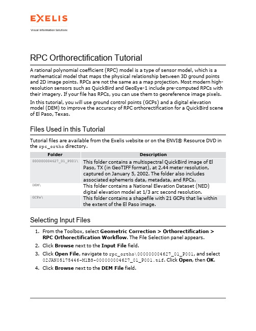
This panel provides some basic details about the GCPs:l The green check marks indicate that these GCPs are active and will be used to adjust the RPC model.These points are called adjustment GCPs.l When you select a GCP in the list,the details of the GCP location appear in the GCP Properties table to the right.Included are the longitude andlatitude in a Geographic Lat/Lon WGS-84projection;height in metersabove the WGS-84ellipsoid;image coordinates;status(adjustment orindependent);and error statistics.The next section will discuss the error statistics in more detail.l The Horizontal Accuracy value is the horizontal root mean square error (RMSE)in meters.In the example above,all of the adjustment GCPs takentogether would yield an orthorectified image that is accurate to within33meters.You will try to reduce this value by assessing the quality of yourGCPs.3.Select GCP1from the list,The image display centers over that point,and theGCP1marker is surrounded by a cyan-colored box.4.Right-click on GCP1in the list,and select Change GCP status.It changesfrom an adjustment GCP to an independent GCP(indicated by a grey diamond symbol).It remains in the GCP list and provides an independent accuracymeasurement,but it will not be used to adjust the RPC model and will notcontribute to the overall model error.Changing the GCP status allows you toturn GCPs on and off without actually deleting them.5.Right-click on GCP1again and select Change GCP status to change it backto an adjustment GCP.Viewing ErrorsIn this section,you will assess the quality of your GCPs and how they contribute to the overall accuracy of the orthorectification,Once you identify GCPs with large errors,you can adjust them or delete them,then re-evaluate the accuracy of the orthorectification.Rather than give a mathematical definition of all of the available error statistics,this tutorial will highlight the most important ones to evaluate and give you a more practical approach to understanding their meaning.For more details on the error statistics,click the Help button in the lower-left corner of the RPC Refinement panel. When the ENVI Help displays,follow the link to"Accuracy Assessment Background."1.In the RPC Refinement panel,click the Show error overlay button.Atransparent image overlays the scene,showing a color gradient of interpolated GCP errors.The darkest areas indicate GCPs with the least error,and the bright red areas indicate GCPs with higher errors.The white area represents a potentially large error with a GCP location.If you scroll to the middle of the GCP list,you will see that GCP14has a green Xmarker.This means that the difference between the image-estimated ground coordinate and the GCP location is greater than three times the root meansquare error in the X or Y direction.The error overlay should look like the following image:The error overlay is useful for quickly evaluating how the GCP errors aredistributed across the entire e the Zoom and Pan tools in the main toolbar to explore the image in more detail if needed.2.In the RPC Refinement panel,select GCP14.The image display centers overthat GCP location.The GCP marker is surrounded by a cyan-colored box in the image display.3.Look at the Error Magnitude value in the GCP Properties pare itsvalue of137.20meters to the Error Magnitude values of other GCPs in the list, and you should see that this GCP does have the highest error.4.From the Zoom To drop-down list in the main toolbar,select1:1,000.5.In the RPC Refinement panel,click the Hide error overlay button to turn offthe error overlay.6.In the RPC Refinement panel,click the Show error vector button.This toolprovides another way to view individual GCP errors.You should see something similar to the following:The cyan-colored vector shows the direction and the magnitude of the error in GCP14.Notice how the vector points to the southwest.If you look at the Error X value in the GCP Properties table,you will see that GCP14shows apredicted difference of-20.98meters between the ground point and thecorresponding image point,in the x-direction.Since the value is negative,the error is to the west.The Error Y value shows a predicted difference of-135.59 meters in the y-direction;since the value is negative,the error is to the south.So both values confirm what the error vector shows.Note:The Error Z value is not shown in the error vector.It represents a predicted differencebetween the Height value of the GCP and the corresponding DEM height above the WGS-84ellipsoid.The length of the cyan-colored vector corresponds to the Error Magnitude value(137.2meters).The red circle around GCP 14shows the circular standard error at the95%confidence level.This means that after you orthorectify the image,you are95% confident that the error of this point will be within this circle.The CE95valueunder the Statistics tab gives the numeric value of this circle,in meters.Correcting ErrorsIf you have more accurate geolocation information available for a given GCP,you can edit its Map X and Map Y values in the GCP Properties table.You can also experiment with different Image X and Image Y values.However,in most cases,it is more practical to interactively move the GCP location in the image display,then re-evaluate its error statistics.1.With the Select icon active in the main toolbar,click and drag the GCP14marker southeast to the starting point of the cyan-colored error vector.The error vector and error overlay both automatically update.You can see from the updated error vector and the Error Magnitude value how the error decreased for this GCP.But how did this affect the overall model?How did the Horizontal Accuracy value change?2.From the Zoom To drop-down list,select Full Extent.Notice how the GCPerrors have been re-computed and how this affects the error overlay.button.。
伍德里奇计量经济学课件 (1)

18
计量经济学
n
若贝尔经济学奖获奖名单
2004 Finn Kydland , Edward Prescott 2003 Robert F. Engle, Clive W. J. Granger 2002 Daniel Kahneman, Vernon L. Smith 2001 George A. Akerlof, A. Michael Spence, Joseph E. Stiglitz 2000 James J Heckman, Daniel L McFadden 1999 Robert A. Mundell 1998 Amartya Sen 1997 Robert C. Merton, Myron S. Scholes 1996 James A. Mirrlees, William Vickrey
INTERMEDIATE ECONOMETRICS
计量经济学导论
Fall, 2012
1
Outline
有关信息 n 什么是计量经济学 n 计量经济学的作用 n 数据: 输入数据 n 经验分析的步骤 n 本课程涵盖的内容
n
2
信息:课程——计量经济学
金融计量学 课号:01663 学分:4 课程性质:教育部规定核心课程
△诺贝尔经济学奖与计量经济学
77位获奖者中10位直接因为对计量经济学发展的贡献而获奖 1969 R. Frish J. Tinbergen 1973 W. Leotief 1980 L. R. Klein 1984 R. Stone 1989 T. Haavelmo 2000 J. J. Heckman D. L. McFadden 2003 R. F. Engle C. W. J. Granger
安然公司事件详细分析案例
丑闻曝光前后的安然公司股价走势
股票价格
➢ 2001年11月30日,股价跌至0.26美元,市值 (800亿元美元-2亿美元)
➢ 2002年1月15日 -股票被摘牌-柜台交易 (90.75-0.07),股东提起集体诉讼
•
踏实肯干,努力奋斗。2021年1月11日 上午10时10分 21.1.1121.1.11
•
追求至善凭技术开拓市场,凭管理增 创效益 ,凭服 务树立 形象。2021年1月11日 星期一 上午10时10分 56秒10:10:5621.1.11
•
严格把控质量关,让生产更加有保障 。2021年1月上 午10时 10分21.1.1110:10Januar y 11, 2021
•
严格把控质量关,让生产更加有保障 。2021年1月上 午10时 10分21.1.1110:10Januar y 11, 2021
•
作业标准记得牢,驾轻就熟除烦恼。2021年1月11日 星期一 10时10分56秒 10:10:5611 January 2021
•
好的事情马上就会到来,一切都是最 好的安 排。上 午10时10分56秒上午10时10分10:10:5621.1.11
有限合伙人
LJM有限 合伙公司
一般合 伙人ຫໍສະໝຸດ ERNB公司 (独立第三方)
投资750万美元
Campsie公司 (独立第三方)
投资750万美元
投资100万美元
LJM开曼有限合伙公司 (LJM1)
应付票据6400万美元
出售340万股安然股票
法斯托先生
为唯一董事
拨付160万股 安然股票和375万美元现金
泛耐药研究进展
[2]Gttdtlctloglu H,Dormaz R,Yaman G,et a1.Spread of a single clone Acinetobacter baumannii strain in an intensive care unit of a teach.
ing
hospital
in
Turkey[J].New Miembiol,2005,28(4):337—43.
基金项目:安徽省优秀青年科技基金(NO:08040106815) 通讯作者:熊自忠,男,博士.教授,研究方向:细菌耐药机制,E-mail: xionI咖zII∞g@126.corn
OXA-23型据石岩等人¨叫报道发现该菌90%基因型 OXA-40型从1995年开始,携带OXA-40基因型的多
为产OXA-23型碳青霉烯酶。
spp;a8
Bergogne-Berezin E.Towner KJ.Acinetobacter
nesocomial
pathogens:mierobiologieal,clinical,and epidemiologieal featur∞
[J].Clin Micrebiol Rev,1996,9(2):148—65. [4】Corbella X,Montero A,Pujol
・6・
安徽医药Anhui Medical
and Pharmaceutical
Journal
2009
Jan;13(1)
泛耐药研究进展
魏艳艳,熊自忠
(安徽医科大学第一附属医院,安徽合肥230022) 关键词:泛耐药;铜绿假单胞菌;鲍曼不动杆菌;碳青霉烯酶 关于泛耐药的定义,不同国家的学者甚至同一国家的学 者都在不断提出新的观点…,但总体趋势的观点是:泛耐药
M1m1mmMMMM1mm1
Issued Date: Feb. 16 2006 Model No.: M190A1-L02 Preliminary 2 / 25 Version 1.0 - CONTENTS - REVISION HISTORY ------------------------------------------------------- 3 1. GENERAL DESCRIPTION ------------------------------------------------------- 5 1.1 OVERVIEW 1.2 FEATURES 1.3 APPLICATION 1.4 GENERAL SPECIFICATIONS 1.5 MECHANICAL SPECIFICATIONS 2. ABSOLUTE MAXIMUM RATINGS------------------------------------------------------- 6 2.1 ABSOLUTE RATINGS OF ENVIRONMENT 2.2 ELECTRICAL ABSOLUTE RATINGS 2.2.1 TFT LCD MODULE 2.2.2 BACKLIGHT UNIT 3. ELECTRICAL CHARACTERISTICS------------------------------------------------------- 8 3.1 TFT LCD MODULE 3.2 BACKLIGHT UNIT 4. BLOCK DIAGRAM------------------------------------------------------- 12 4.1 TFT LCD MODULE 4.2 BACKLIGHT UNIT 5. INPUT TERMINAL PIN ASSIGNMENT------------------------------------------------------- 13 5.1 TFT LCD MODULE 5.2 BACKLIGHT UNIT 5.3 COLOR DATA INPUT ASSIGNMENT 6. INTERFACE TIMING ------------------------------------------------------- 16 6.1 INPUT SIGNAL TIMING SPECIFICATIONS 6.2 POWER ON/OFF SEQUENCE 7. OPTICAL CHARACTERISTICS ------------------------------------------------------- 18 7.1 TEST CONDITIONS 7.2 OPTICAL SPECIFICATIONS 8. PACKAGING------------------------------------------------------- 21 8.1 PACKING SPECIFICATIONS 8.2 PACKING METHOD 9. DEFINITION OF LABELS------------------------------------------------------- 23 10. PRECAUTIONS------------------------------------------------------- 24 10.1 ASSEMBLY AND HANDLING PRECAUTIONS 10.2 SAFETY PRECAUTIONS 11. MECHANICAL CHARACTERISTICS ------------------------------------------------------- 25 Issued Date: Feb.16 2006 Model No.: M190A1-L02 Preliminary 3 / 25 Version 1.0 REVISION HISTORY Version Date S ection Description 0.0 1.0 Jan 20 06’ Feb 16 06’ All 7.2 9.1 M190A1-L02 Specifications was first issued. Optical specifications: Typ: RxRy: 0.6360.3490.6400.335 GxGy: 0.2900.589 0.2830.599 BxBy: 0.1430.080 0.1530.079Contrast Ratio :Min TBD 600 Typ 800 850 Viewing angle: Min Typ : θx 7080 7585 θx- 7080 7585 Update module label wording amp model name from L01 to L02 Issued Date: Feb.16 2006 Model No.: M190A1-L02 Preliminary 4 / 25 Version 1.0 1. GENERAL DESCRIPTION 1.1 OVERVIEW M190A1-L02 is a 19” w ide TFT Liquid Crystal Display module with 4 CCFL Backlight unit and 30 pins 2ch-LVDS interface. This module supports 1440 x 900 WXGA mode and can display 16.2M colors. The inverter module for Backlight is not built in. 1.2 FEATURES - Super Wide viewing angle. - Super High contrast ratio - Super fast response time - High color saturation - WXGA 1440 x 900 pixels resolution - DE Data Enable only mode - LVDS Low Voltage Differential Signaling interface - RoHS Compliance 1.3 APPLICATION - TFT LCD Monitor 1.4 GENERAL SPECIFICATI0NS Item Specification Unit Note Diagonal Size 481.4 19.05” diagonal mm Active Area 410.4 H x 256.5 V mm Bezel Opening Area 414.36 x 260.45 mm 1 Driver Element a-si TFT active matrix - - Pixel Number 1440 x R.G.B. x 900 pixel - Pixel Pitch 0.285 H x 0.285 V mm - Pixel Arrangement RGB vertical stripe - - Display Colors 16.2M color - Transmissive Mode Normally White - - Surface Treatment Hard coating 3H Anti-glare Haze 25 - - 1.5 MECHANICAL SPECIFICATIONS Item Min. Typ. Max. Unit Note HorizontalH 426.7 427.2 427.7 mm VerticalV 276.9 277.4 277.9 mm Module Size DepthD - 17 17.5 mm 1 Weight - - 2500 g- Note 1 Please refer to the attached drawings for more information of front and back outline dimensions. Issued Date: Feb. 16 2006 Model No.: M190A1-L02 Preliminary 5 / 25 Version 1.0 2. ABSOLUTE MAXIMUM RATINGS 2.1 ABSOLUTE RATINGS OF ENVIRONMENT Value Item SymbolMin. Max. Unit Note Storage Temperature TST-20 60 ??C 1 Operating Ambient Temperature TOP 0 50 ??C 1 2 Shock Non-Operating SNOP - 50 G 3 5 Vibration Non-Operating VNOP - 1.5 G 4 5 Note 1 Temperature and relative humidity range is shown in the figure below. a 90 RH Max. Ta ≤ 40 ??C. bWet-bulb temperature should be 39 ??C Max. Ta gt 40 ??C. c No condensation. Note 2 The temperature of panel display surface area should be 0 ??C Min. and 60 ??C Max. Note 3 11ms half sine wave 1 time for ± X ± Y ± Z. Note 4 10 300 Hz 10min/cycle 3 cycles each X Y Z. Note 5 At testing Vibration and Shock the fixture in holding the module has to be hard and rigid enough so that the module would not be twisted or bent by the fixture. Side Mount Fixing Screw Side Mount Fixing Screw Stage BracketLCD Module Gap2mm At Room TemperatureStorage Range Relative Humidity RH Operating RangeTemperature ??C 10080 60 -20 400 20-40 8040602010 90 Issued Date: Feb. 16 2006 Model No.: M190A1-L02 Preliminary 6 / 25 Version 1.0 2.2 ELECTRICAL ABSOLUTE RATINGS 2.2.1 TFT LCD MODULE Value Item Symbol Min. Max. Unit Note Power Supply Voltage Vcc -0.3 6.0 V Logic Input Voltage VIN -0.3 4.3 V 1 2.2.2 BACKLIGHT UNIT Value Item Symbol Min. Max. Unit Note Lamp Voltage VL - 2.5K VRMS 1 2 IL 7.0mA Lamp Current IL - 7.5 mARMSLamp Frequency FL - 80 KHz 1 2 Note 1 Permanent damage to the device may occur if maximum values are exceeded. Function operation should be restricted to the conditions described under Normal Operating Conditions. Note 2 Specified values are for lamp Refer to 3.2 for further information. Issued Date: Feb. 16 2006 Model No.: M190A1-L02 Preliminary 7 / 25 Version 1.0 3. ELECTRICAL CHARACTERISTICS 3.1 TFT LCD MODULE Ta 25 ±2 ??C Value Parameter SymbolMin. Typ. Max. Unit Note Power Supply Voltage Vcc 4.5 5.0 5.5 V - Ripple Voltage VRP - - 100 mV - Rush Current IRUSH- 1.6 3 A 2 White 0.5 0.7 A 3a Black 0.7 1.0 A 3b Power Supply Current Vertical Stripe - - - 0.7 1.0 A 3c LVDS differential input voltage Vid 100 - 600 mV LVDS common input voltage Vic - 1.2 - V Logic “L” input voltage Vil Vss - 0.8 V Note 1 The module should be always operated within above ranges. Note 2 Measurement Conditions: Vcc rising time is 470??s 470??s5.0V GND 0.9Vcc 0.1Vcc R1 High to Low Control Signal 12V SW Q2C1 1uF Vcc 5.0V 2SK1470Q12SK147547K R2 1K VR1 47K C20.01uFC3 1uF FUSELCD Module Input Issued Date: Feb. 16 2006 Model No.: M190A1-L02 Preliminary 8 / 25 Version 1.0 Note 3 The specified power supply current is under the conditions at Vcc5.0 V Ta 25 ± 2 ??C fv 60 Hz whereas a power dissipation check pattern below is displayed. Active Area a. White Pattern Active Area c. Vertical Stripe Pattern R R R R B B B B BBGGGGActive Area b. Black Pattern Issued Date: Feb. 16 2006 Model No.:M190A1-L02 Preliminary 9 / 25 Version 1.0 3.2 BACKLIGHT UNIT Ta 25 ± 2 ??C Value Parameter Symbol Min. Typ. Max. Unit Note Lamp Input Voltage VL 697 775 853 VRMS IL 7.0 mA Lamp Current IL 2.0 7.0 7.5 mARMS 1 --- --- 150025℃VRMS 2 Lamp Turn On Voltage VS --- --- 17100℃VRMS 2 Operating Frequency FL 40 --- 80 KHz 3 Lamp Life Time LBL 40000 --- --- Hrs 5 Power Consumption PL --- 21.72 --- W 4 IL 7.0 mANote 1 Lamp current is measured by utilizing high frequency current meters as shown below: Note 2 The voltage shown above should be applied to the lamp for more than 1 second after startup. Otherwise the lamp may not be turned on. Note 3The lamp frequency may produce interference with horizontal synchronous frequency from the display and this may cause line flow on the display. In order to avoid interference the lamp frequency should be detached from the horizontal synchronous frequency and its harmonics as far as possible. Note 4 PL IL ×VL × 4 CCFLs Note 5 The lifetime of lamp can be defined as the time in which it continues to operate under the condition Ta 25 ±2 oC and IL 7.0 mA rms until one of the following events occurs: a When the brightness becomes or lower than 50 of its original value. b When the effective ignition length becomes or lower than 80 of its original value. Effective ignition length is defined as an area that has less than 70 brightness compared to the brightness in the center point. Note 6 The waveform of the voltage output of inverter must bearea-symmetric and the design of the inverter must have specifications for the modularized lamp. The performance of the Backlight such as lifetime or brightness is greatly influenced by the characteristics of the DC-AC inverter for the lamp. All the parameters of an inverter should be carefully designed to avoid producing too much current leakage from high voltage output of the inverter. When designing or ordering the inverter please make sure that a poor lighting caused by the mismatch of the Backlight and the inverter miss-lighting flicker etc. never occurs. If the above situation is confirmed the module should be operated in the same manners when it is installed in your instrument. LCD ModuleInverter1AHV Pink 2LV White Current Meter YOKOGAWA 2016A 1AHV Blue 2LV Black Issued Date: Feb. 16 2006 Model No.: M190A1-L02 Preliminary 10 / 25 Version 1.0 The output of the inverter must have symmetrical negative and positive voltage waveform and symmetrical currentwaveform.Unsymmetrical ratio is less than 10 Please do not use the inverter which has unsymmetrical voltage and unsymmetrical current and spike wave. Lamp frequency may produce interface with horizontal synchronous frequency and as a result this may cause beat on the display. Therefore lamp frequency shall be as away possible from the horizontal synchronous frequency and from its harmonics in order to prevent interference. Requirements for a system inverter design which is intended to have a better display performance a better power efficiency and a more reliable lamp. It shall help increase the lamp lifetime and reduce its leakage current. a. The asymmetry rate of the inverter waveform should be 10 below b. The distortion rate of the waveform should be within √2 ± 10 c. The ideal sine wave form shall be symmetric in positive and negative polarities. I p I -p Asymmetry rate: I p – I –p / Irms 100 Distortion rate I p or I –p / Irms Issued Date: Feb. 16 2006 Model No.: M190A1-L02 Preliminary 11 / 25 Version 1.0 4. BLOCK DIAGRAM 4.1 TFT LCD MODULE 4.2 BACKLIGHT UNIT TFT LCD PANEL1440x3x900 DATA DRIVER ICSCAN DRIVER IC BACKLIGHT UNIT LVDS INPUT / TIMING CONTROLLERDC/DC CONVERTER ampREFERENCE VOLTAGE INPUT CONNECTOR JAE-FI-XB30SRL-HF11 GND VL Vcc RXO0/- RXO1/- RXO2/- RXO3/- RXOC/- RXE0/- RXE1/- RXE2/- RXE3/- RXEC/- LAMP CONNECTOR JST-BHSR-02VS-1 1 HVBlue 2 LVBlack 1 HVPink 2 LVWhite 1 HVBlue 2 LVBlack 1 HVPink 2 LVWhiteNC Issued Date: Feb. 16 2006 Model No.:M190A1-L02 Preliminary 12 / 25 Version 1.0 5. INPUT TERMINAL PIN ASSIGNMENT 5.1 TFT LCD MODULE Pin Name Description 1 RXO0- Negative LVDS differential data input. Channel O0 odd 2 RXO0 Positive LVDS differential data input. Channel O0 odd 3 RXO1- Negative LVDS differential data input. Channel O1 odd 4 RXO1 Positive LVDS differential data input. Channel O1 odd 5 RXO2- NegativeLVDS differential data input. Channel O2 odd 6 RXO2 Positive LVDS differential data input. Channel O2 odd 7 GND Ground 8 RXOC- Negative LVDS differential clock input. odd 9 RXOC Positive LVDS differential clock input. odd 10 RXO3- Negative LVDS differential data input. Channel O3odd 11 RXO3 Positive LVDS differential data input. Channel O3 odd 12 RXE0- Negative LVDS differential data input. Channel E0 even 13 RXE0 Positive LVDS differential data input. Channel E0 even 14 GND Ground 15RXE1- Negative LVDS differential data input. Channel E1 even 16 RXE1 Positive LVDS differential data input. Channel E1 even 17 GND Ground 18 RXE2- Negative LVDS differential data input. Channel E2 even 19 RXE2 Positive LVDS differential data input. Channel E2 even 20 RXEC- Negative LVDS differential clock input. even 21 RXEC Positive LVDS differential clock input. even 22 RXE3- Negative LVDS differential data input. Channel E3 even 23 RXE3 Positive LVDS differential data input. Channel E3 even 24 GND Ground 25 NC Not connection. 26 NC Not connection. 27 NC Not connection. 28 VCC 5.0V power supply 29 VCC 5.0V power supply 30 VCC 5.0V power supply Note 1 Connector Part No.: JAE-FI-XB30SRL-HF11 or equivalent. Note 2 The first pixel is odd. Note 3 Input signal of even and odd clock should be the same timing. Issued Date: Feb. 16 2006 Model No.: M190A1-L02 Preliminary 13 / 25 Version 1.0 LVDS output D7 D6 D4 D3 D2 D1 D0 LVDS Channel E0 Data order EG0 ER5 ER4 ER3 ER2 ER1 ER0 LVDS output D18 D15 D14 D13 D12 D9 D8 LVDS Channel E1 Data order EB1 EB0 EG5 EG4 EG3 EG2 EG1 LVDS output D26 D25 D24 D22 D21D20 D19 LVDS Channel E2 Data order DE NA NA EB5 EB4 EB3 EB2 LVDS outputD23 D17 D16 D11 D10 D5 D27 LVDS Channel E3 Data order NA EB7 EB6 EG7 EG6 ER7 ER6 LVDS output D7 D6 D4 D3 D2 D1 D0 LVDS Channel O0 Data order OG0OR5 OR4 OR3 OR2 OR1 OR0 LVDS output D18 D15 D14 D13 D12 D9 D8 LVDS Channel O1 Data order OB1 OB0 OG5 OG4 OG3 OG2 OG1 LVDS output D26 D25D24 D22 D21 D20 D19 LVDS Channel O2 Data order DE NA NA OB5 OB4 OB3 OB2 LVDS output D23 D17 D16 D11 D10 D5 D27 LVDS Channel O3 Data order NA OB7 OB6 OG7 OG6 OR7 OR6 Issued Date: Feb. 16 2006 Model No.: M190A1-L02 Preliminary 14 / 25 Version 1.0 5.2 BACKLIGHT UNIT Pin Symbol Description Remark 1 HV High Voltage Pink 2 LV Low Voltage White 1 HV High Voltage Blue 2 LV Low Voltage Black Note 1 Connector Part No.: BHSR-02VS-1 JST or equivalent Note 2 User’s connector Part No.:SM02B-BHSS-1-TB JST or equivalent 5.3 COLOR DATA INPUT ASSIGNMENT The brightness of each primary color red green and blue is based on the 8-bit gray scale data input for the color. The higher the binary input the brighter the color. The table below provides the assignment of color versus data input. Data Signal Red Green Blue Color R7R6 R5 R4 R3R2R1R0R7R6G5G4G3G2G1G0 R7 R6 B5 B4 B3B2B1B0Basic Colors Black Red Green Blue Cyan Magenta Yellow White 010001110 1 0 0 0 1 1 1 0 1 0 0 0 1 1 1 0 1 0 0 0 1 1 1 010001110100011101000111010001110010101100101011001010110010101100101011 00101011001010110 0 1 0 1 0 1 1 0 0 0 1 1 1 0 1 0 0 0 1 1 1 0 1 0 0 0 1 1 1 0 1 0 0 0 1 1 1 0 1 00011101000111010001110100011101 Gray Scale Of Red Red0 / Dark Red1Red2 : : Red253 Red254 Red255 000::1110 0 0 : : 1 1 1 0 0 0 : : 1 1 1 0 0 0 : : 1 1 1 000::111000::111001::011010::101000::000000::000000::000000::000000::000000::000 000::0000 0 0 : : 0 0 0 0 0 0 : : 0 0 0 0 0 0 : : 0 0 0 0 0 0 : : 0 0 0 0 0 0 : : 0 0 0000::000000::000000::000000::000 Gray Scale Of Green Green0 / Dark Green1Green2 : : Green253 Green254 Green255 000::0000 0 0 : : 0 0 0 0 0 0 : : 0 0 0 0 0 0 : : 00 0 000::000000::000000::000000::000000::111000::111000::111000.。
Chapter_07
Willy Sansen
10-05
0710
Symmetrical CMOS OTA
M7 1: M9 :1
VDD
M8 4
Differential pair 3 Current mirrors
5
M1 2
3
+
M2 1
vOUT
CL
Symmetrical : Node 1 = Node 2 Rail-to-rail output swing
fnd = ≈
gm3 2π Cn1 fT3NPN 3
2
1
M10
M11
VSS
Higher !
Willy Sansen
10-05
0728
Folded cascode OTA: input to Vss rail
M9 M5 7 M7 5 M6 6 M8 4
VDD
M1
0.9 V
3
+
M2
vOUT
CL
VT = 0.7 V VGS1-VT = 0.2 V VGS10-VT = 0.5 V V+ = 1.5 V VGS3-VT = 0.2 V
Willy Sansen 0723
10-05
Folded cascode CMOS OTA : DC
M9
VDD
50
M2
50
100
M1
DC current flow
-
3
+ +
M4
vOUT
50 50 100 100
M11
2
50 1 50
CL
VSS
Willy Sansen
10-05