Power Semiconductor Devices ch1-3
LA4601N中文资料
1.0 µF 0.2s
2.2 µF 0.3s
3.3 µF 0.5s
4.7 µF 0.65s
10 µF 1.5s
3. Filter (decoupling) pin (5)
Pin voltage is approx. 1/2 VCC. The recommended value for the filter capacitor is 100 µF. When capacitance is lower, pop noise when setting the standby pin to Low (power OFF) will increase.
SANYO assumes no responsibility for equipment failures that result from using products at values that exceed, even momentarily, rated values (such as maximum ratings, operating condition ranges, or other parameters) listed in products specifications of any and all SANYO products described or contained herein.
(ts). (The starting time is the time required from applying voltage to the standby pin until sound output is obtained.)
Input capacitator Starting time (ts)
12
电力电子技术基础(英文) 蒋晓华Cha1Devices
1-3. GTO (Gate Turn-off Thyristor)
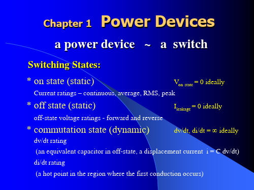
Power Devices
A reverse voltage with the cathode positive will break down the anode junction at a low level.
Won--- major loss at lower-frequency operation Wswitch--- significant at high-frequency operation
Power Devices
A POWER SWITCHING DEVICE
* permits current flow in one direction only * can withstand a forward voltage (except diodes) * can be turned on or off
1-2. Thyristor (SCR)
Ib1
+ Anode
Ia
P
Power Devices
Structure and symbol
N
Ib2 AnGodatee
P Ig N
Ic
- Cathode
IgIb1
Ia, Ic
Cathode
Ib2
ChaCrhaactreaPrcoitssetiritciisvtewicfisetehwdinbtohacgkate current
Power Devices
Wstatic =Won+ Woff = on-time ion(t)von-state(t)dt + off-time ileakage(t)voff(t)dt
第1章 电力电子器件概述54154精品

又称整流二极管(Rectifier Diode) 多用于开关频率不高(1kHz以下)的整流电路 其反向恢复时间较长 正向电流定额和反向电压定额可以达到很高 DATASHEET
1-23
1.2.4 电力二极管的主要类型
2) 快恢复二极管 (Fast Recovery Diode——FRD)
主电路(Main Power Circuit)
——电气设备或电力系统中,直接承担电能的变换或控 制任务的电路。
2)分类:
电真空器件 (汞弧整流器、闸流管)
半导体器件 (采用的主要材料硅)仍然
1-5
1.1.1 电力电子器件的概念和特征
3)同处理信息的电子器件相比的一般特征:
能处理电功率的能力,一般远大于处理信息的电子 器件。 电力电子器件一般都工作在开关状态。 电力电子器件往往需要由信息电子电路来控制。 电力电子器件自身的功率损耗远大于信息电子器件, 一般都要安装散热器。
图1-5(b)关断过程
开通过程:
u i
正向压降先出现一个过冲UFP,经 UFP
iF
过一段时间才趋于接近稳态压降的
某个值(如 2V)。
2V
uF
正向恢复时间tfr。 电流上升率越大,UFP越高 。
0
tfr
t
图1-5(b)开通过程
1-19
1.2.3 电力二极管的主要参数
1) 正向平均电流IF(AV) 额定电流——在指定的管壳温度和散热 条件下,其允许流过的最大工频正弦半 波电流的平均值。 IF(AV)是按照电流的发热效应来定义的,使 用时应按有效值相等的原则来选取电流 定额,并应留有一定的裕量。
本章小结及作业
模拟电路分析与设计英文pptch1

Ch1. Semiconductor Materials and Diodes
1.1 Semiconductor Materials and Properties 1.2 The PN Junction 1.3 Diode Circuits DC Analysis and Models 1.4 Diode Circuits AC Equivalent Circuit 1.5 Other Diode Types 1.6 Design Application: Diode Thermometer 1.7 Summary
+4
+4
+4
+4
Each Si atom shares one electron with each of its four closest neighbors so that its valence band will have a full 8 electrons.
新编文档-模拟电路分析与设计英文pptch1-精选文档-精品文档
+4
+4
+4
+4
Each Si atom shares one electron with each of its four closest neighbors so that its valence band will have a full 8 electrons.
1.1.1 Intrinsic Semiconductor
Increasing temperature, generating electron-hole pairs
Carriers
• Free electron---produced by thermal ionization. It can move freely in the lattice structure so as to form current.
2. When T increases, free electrons and “holes”are created • In pure semiconductor, the concentration of electrons and holes are equal, and very small, so it has very small conductivity.
1.1 Semiconduct 1.1.1. Intrinsic Semiconductor
Materials
Conductor : conduction electrons__electrical conductivity Insulator : electrons in bonding mechanism __cannot move Semiconductor : silicon, germanium, gallium arsenide
Smar PS-AC-R 电源模块 90-264 VAC输入说明书

PS-AC-RUSER’S MANUALPS-AC-RPower Supply Module 90 to 264 Vac InputP S A C R M EsmarSpecifications and information are subject to change without notice.Up-to-date address information is available on our website.PS-AC-R - Power Supply Module - 90 to 264 Vac Input3AVOIDING ELECTRICAL DISCHARGESElectrostatic discharges may damage semiconductor electronic components in printed circuitboards. They usually occur when touching components or connector pins from modules and racks, without wearing the appropriate equipment to prevent discharges. It is recommended to take the following precautions:• Before handling modules and racks, remove the electrostatic charge from your body bywearing a proper wristband or touching grounded devices;• Avoid touching electronic components or connector pins from racks and modules.PS-AC-R - User’s Manual4 PS-AC-R - POWER SUPPLY MODULE - 90 TO 264 VAC INPUT - REDUNDANTDescriptionThis redundant power supply works independently or in together with other redundant power supplymodule to ensure a constant supply of power to the application.When two redundant power supplies are used, if one of them fails, the backup will automaticallyassume the operation. A relay is provided to indicate failure on each power supply giving the user achance to replace the faulty one.This module provides two voltage outputs:5 Vdc @ 3 A: distributed by Power Lines in the Inter-Module-Bus (IMB) throughout the racks tosupply the module circuits;24 Vdc @ 300 mA: for external use through the terminals 1B and 2B.The applied AC voltage, the 5 Vdc and the 24 Vdc are all isolated between them. Installation and ConfigurationFor systems based on DF93 rack, with DF90 and DF91Redundant mode options•Splitting Power concept: In this situation, two modules will supply power to a bus segment. Ifone of them was turned off or fails, the other power supply must be able to supply energy,alone, to the segment.The CH1jumper (power supply) must be set in R position for both modules and W1jumper(power supply) must be opened for both modules.•Standby concept: In this case, just one power supply provides energy to the system. If it wasturned off or fails, the backup module will assume the operation. In both modules, the jumperCH1(power supply) must be set in the R position and W1jumper (power supply) must beplaced only in the backup module.Expansion of load capacity by adding power suppliesIf the system consumption is greater than 3A, it can be subdivided in up to 8 groups sized forconsumption of up to 3A each, and each group is individually powered by a power supply. Moredetails on the Power supplies positioning topic. In the power supply module the CH1 jumper must beset in E position.Power supplies positions in the racksOn DF93 is recommended the placement of the redundant pair in the first and second slots, but itcan be installed in any slots if necessary.For systems based on R-700-4A rackNon-redundant (single module) - power consumption limited to 3AThere is an addressing restriction related to the power supply location. The restriction is that the firstrack (address 0) must always contain a power supply module at the first slot. In the power supplymodule the CH1 jumper must be set in E position.PS-AC-R - Power Supply Module - 90 to 264 Vac Input5Non-redundant (more than one module) - power consumption bigger than 3AAdditional modules are placed in the bus in parallel, but isolated one of the other. For systems based on R-700-4A rack, the power supplies modules must always be placed at the first rack’s slot. The jumper W1 (in the rack), where is the new power supply module, must be cut. The new power supply module will only supply power to the rack where it is sitting on and to the consecutive ones (never backwards).In all power supplies modules, the CH1 jumper must be set in E position.Redundant mode :- Split power concept: In this case of redundancy, the user may have two power supplies modules in parallel in first and third slots of rack R-700-4A . The CH1 jumper (power supply) must be set in R position in both modules and W1 jumper (power supply) must be opened in both modules. In this situation, the two modules will supply power to the bus.- Standby concept: In this case, the main module must be placed in the first slot and the backup module in the third slot of rack R-700-4A . In both modules, the jumper CH1 must be set in the position R and W1AC Power Supply Module: PS-AC-RTechnical specificationsINPUTSDC 127 to 135 VdcAC90 to 264 Vac, 50/60 Hz (nominal), 47 to 63 Hz (range) Inrush Current < 36 A @ 220 Vac. [∆T < 740 μs]Time until Power Fail 6 ms @ 102 Vac (120 Vac – 15%) [Full Load] Time until Shutdown 27 ms @ 102 Vac; > 200 ms @ 220 Vac [Full Load] Maximum Consumption 72 VAIndicatorAC LINE (Green LED)PS-AC-R - User’s Manual6 a)Output 1 (internal use) 5.2 Vdc +/- 2%Current 3 A MaximumRipple 100 mVpp MaximumIndicator +5 Vdc (Green LED)Hold up time > 40 ms @ 120 Vac [Full Load]b) Output 2 (external use) 24 Vdc +/- 10%Current 300 mA MaximumRipple 200 mVpp MaximumShort circuit current 700 mAIndicator +24 Vdc (Green LED)Input, internal output and external output signals are isolated between them.Between outputs and ground 1000 VrmsBetween input and output 2500 VrmsType of Output Solid state relay, normally closed (NC), isolatedLimits 6 W, 30 Vdc max, 200mA maxMaximum Initial ContactResistance<13ΩOverload Protection Should be provided externallyOperation Time 5 ms maximumOperation -10 °C to 60 °C (14 ºF to 140 ºF)Dimensions (L X H X D)39.9 x 137.0 x 141.5 mm(1.57 x 5.39 x 5.57 in)Weight 0.450 kgOne wire 14 AWG (2 mm2)Two wires 20 AWG (0.5 mm2)1) If the power consumption exceeds the power supplied, the system may operate in anunpredictable manner that may causes damages to the equipment or risk of personal injury.Hence, the power consumption must be calculated correctly and install more power supplies modules, if it is necessary.2) To increase the service life of your contacts and protect the modules from potential reversevoltage damage, connect externally a clamping diode in parallel with each inductive DC load or connect a RC snubber circuit in parallel with each inductive AC load.3) To meet the EMC standards requirements, the wires’ length to the failure relay must be lessthan 30 meters. The power supply of activated load by the failure relay must not be from external network.4) The redundancy feature is only guaranteed for racks with GLL1270 Revision 2 or greater.For the models with their revisions less than the mentioned above, the technical support must be consulted in order to check the compatibility.PS-AC-R - Power Supply Module - 90 to 264 Vac Input Calculating the Power ConsumptionSince the power available from the power supply is limited, it is important to calculate the modulespower consumption that will be used. One way of doing that is constructing a sheet to summarize allcurrent supplied and required from each module and the associated devices (such as operatorinterface). And then, to calculate the maximum current required and the maximum current supplied.If “maximum current required” is greater than “current supplied” the power consumption will beexceeded. If this is the case, it will be unsafe to use this configuration and you will need to reviewthe system design or add more power supply modules through out the racks.However, CONF700software for LC700offers the fastest way to obtain the total powerconsumption for an application. Once the modules in the Hardware Page have been selected, thepower consumption report is immediately available. To learn how to use this feature of CONF700,refer to the LC700 Configuration Manual for further information.The Power Supply Concept of a LC700 SystemIf the LC700 needs more power supply modules, each one of the power supply modules will providecurrent up to the maximum value of modules located on its right-hand side. The following steps willhelp you to understand how many power supply modules are required for the LC700 system:•Observe the maximum current values from the power supply module specification.•Be sure that the consumption of the modules to the right of the power supply does notexceed the maximum value.•Follow the steps in the next topic if the power consumption exceeds the limit.To add a new power supply module•Determine the rack where the new power supply will be installed.•Cut the jumper W1 located on the rack.•Plug the new power supply at the first slot of the rack (Slot 0).•In this case the CH1 of all PS-AC-R modules must be set in E position.Power supplies positioningFor systems based on DF93 rack with DF90 and DF91A power supply connected to a rack, in a system, provides current to the racks row that arehorizontally interconnected to it by their terminals of lateral connections, and vertically through DF90cables, thus forming a group of rows of racks that use the same power supply.The system can have only one power supply or it can be subdivided in several of these groups1,each one powered by a power supply.The recommended way to distribute the power is to divide the system in groups of horizontal rows ofracks. In this scheme, each power supply must be positioned on the top left of the group of rows ofracks that it powers. The rack were is the power supply must be the W1 jumper cut and the DF90cable must not be connected to the rows powered by other power supplies (top rows). See in thefollowing figure an example of system powered by two power supplies, each one powers a part ofrows represented in green and blue.1 Maximum 8 groups allowed when the PS-AC-R power supplies are used.7PS-AC-R - User’s Manual8System powered by two power suppliesNote that this system, for greater efficiency, is optimized for power distribution by groups of rows of racks. Thus, a power supply powers a whole number of rows it supports. However, in rare cases, with long rows or many modules with great consumption in the same row, there is the option to add power supplies in the middle of the row, dividing the power within this row. In this case, the power supply added powers only the modules positioned on the right in the same row, up to the end, or even where there is another power supply added. In the rack where the power supply was added, in this scheme, the W1 jumper must be cut and left lateral connection terminal (+5 Vdc) must be disconnected (collapsed).In this system, PS-AC-R modules must be their CH1 jumper always configured in E .ATTENTIONA mixture of these power supplies with the CH1 configured in R and in E in any LC700 system, is not allowed!On DF93 is recommended the placement of the redundant pair in the first and second slots, but it can be installed in any slots if necessary.The system has diagnostic for voltage level distributed to racks. It also supports modules with great power consumption in any place on the bus. Nevertheless, is recommended to place those modules close to the power supplies, to avoid unnecessary power transmission.For systems based on R-700-4A rack1. Observe the maximum current values from the power supply module specification. The limit forPS-AC-R is 3 A.2. After the connection with long cables (FC-700-1A , FC-700-2A , FC-700-3A and/or FC-700-4A )you have to put another power supply module in the first slot of the first rack.3. Use up to 6 modules M-401-R/M-401-DR per power supply; always place the M-401-R/M-401-DR consecutively and close to the power supply. Because of the high current consumption of the modules M-401-R/M-401-DR , a not desired voltage drop in the bus can occur if these modules are placed after other modules.PS-AC-R - Power Supply Module - 90 to 264 Vac Input 4. When is necessary to add interface modules, such as MB700and SI-700, in the same buswhich is used by output and input modules, is recommended that these modules are placed close to the power supply, because in the same way as described in the previous item, a not desired voltage drop in the bus can occur if these modules are placed after other modules.5. Adding a new power supply module•Determine the rack where the new power supply will be installed.•Cut the jumper W1 of the rack.•Plug the new power supply at the first slot of the rack (slot 0).•In this case, the CH1 jumper of all PS-AC-R modules must be set in E position.9PS-AC-R - User’s Manual10Installing Modules in the RackFollow the steps below to install a module in the rack.Attach the top of the module (with a 45oinclination) to the module support located on the upper part of the rack.Mounting detail.Push the module fixing it to the module connector.Next, fix the module to the rack using a screwdriver, and fasten the fixation screw at the bottom of the module.Appendix AA.1PS-AC-R - User’s Manual A.2。
电气工程及其自动化专业英语 Chapter 3 Power Electronic Technology
Section 1 Semiconductor Switches
over, the diode Vl begins to conduct and the voltage on the switch is clamped at Uo, and the current through the switch ramps linearly (again an assumption) down to zero. When the switch is closed, the current begins to build up linearly to IS while the diode V1 is still on. The voltage on the switch remains clamped at UO. After the switch current reaches IS, the diode turns off and the voltage on the switch begins to ramp down to zero.
Semiconductor switches are very important and crucial components in power electronic systems. These switches are meant to be the substitutions of the mechanical switches, but they are severely limited by the properties of the semiconductor materials and the process of manufacturing.
Section 1 Semiconductor Switches
Semiconductor_physics_and_devices_B1课堂PPT
– §1.1crystal structure 晶体结构
• lattice 晶格 • basic vector 基矢 • unit cell 元胞 • 3 basic cubic structure (simple cubic, body-centered cubic, face-
Catalog
• goal
– to equip the students with the essential theory of semiconductor physics, devices and skills of ICs design
– to make them well prepared for the design of semiconductor devices or integrated circuits.
Introduction 绪论
• A semiconductor is a kind of conductor. 半导体——导体的一种
• introduction:
– The relation between semiconductor materials and devices or ICs,半导体材料与器件或集成电路的关系
•6
Function and objectives:
• Function
– core course for advanced courses of various specialties of information, such as electronic Science and Technology, Telecommunication and automation
第1章 电力电子器件53958
1.1.3 电力电子器件的分类
➢ 按照器件能够被控制电路信号所控制的程度, 分为以下三类:
1) 半控型器件
➢ 晶闸管(Thyristor)及其大部分派生器件
通➢ 过器控件制的信关断号由可其以在控主制电路其中导承通受而的不电压能和控电制流其决关定 断。
2) 全控型器件
➢ 绝 缘 栅 双 极 晶 体 管 ( Insulated-Gate Bipolar
P型区
- + ·+ ·+ ·+
- + ·+ ·+ ·+
- + ·+ ·+ ·+
- + ·+ ·+ ·+
- + ·+ ·+ ·+
空间电荷区
N型区
图1-3 PN结的形成
• 扩空交散间界运电处动荷电和建子漂立和移的空运电穴动场的最被浓终称度达为差到别内动,电态造场平 成或衡了自,各建正区电、的场负多,子 空其向间方另电向一荷是区量阻的达 止扩到扩散稳散运定运动值动,,的到形,对成另方了一区一方内个面成稳又为定吸少的引子由对,空方在间区界面 电内两荷的侧构少分成子别的(留范 对 下围本了,区带被而正称言、为则负为电空多荷间子但电)不荷向能区本任,区意按运移所动强,的调即杂的质 角漂离度子移不。运同这动也些。被 不称能为移动耗的尽正层、负阻电挡荷层称或为势空垒间区电。荷。
当电力二极管的外加电压由正 向变为反向,正向电流在此反向电 压的作用下开始下降至零后,由于 二极管在PN结两侧储存了大量少 子因而并没有恢复反向阻断能力, 这些少子在外加反向电压的作用下 被抽取出电力二极管,因而形成交 大的反向电流,并伴随有明显的反 向过冲电压,当反向电流的变化率 接近于零后,电力二极管两端承受 的电压降至外加电压的大小,电力 二极管完全恢复对反向电压的阻断 能力。这就是二极管的反向恢复过 程。
功率器件Power Electronic Devices
Major topics for each device Appearance, structure, and symbol Physics of operation Specification Special issues Devices of the same family
Passive components in power electronic circuit Transformer, inductor, capacitor and resistor: these are passive components in a power electron ic circuit since they can not be controlled by control signal and their characteristics are usually constant and linear. The requirements for these passive components by power electronic circuits could be very different from those by ordinary circuits.
1.2 Uncontrolled device Power diode
Appearance
PN junction
Direction of inner electric field
Region (depletion region, potential barrier region)
+ + + + +
Very often: Power electronic devices= Power semiconductor devices Major material used in power semiconductor devices——Silicon