ARM 24B-920t中文文档
AT91RM9200中文手册(修正版)

1特性•融合了ARM920T ™ ARM ® Thumb ®处理器–工作于180 MHz 时性能高达200 MIPS ,存储器管理单元–16-K 字节的数据缓存,16-K 字节的指令缓存,写缓冲器–含有调试信道的内部仿真器–中等规模的嵌入式宏单元结构(仅针对256 BGA 封装)•低功耗:VDDCORE 电流为30.4 mA 待机模式电流为3.1 mA •附加的嵌入式存储器–SRAM 为16K ;ROM 为128K •外部总线接口(EBI)–支持SDRAM ,静态存储器, Burst Flash ,无缝连接的CompactFlash ®,SmartMedia ™及NAND Flash •提高性能而使用的系统外设:–增强的时钟发生器与电源管理控制器–两个有双PLL 的片上振荡器–低速的时钟操作模式与软件功耗优化能力–四个可编程的外部时钟信号–包括周期性中断、看门狗及第二计数器的系统定时器–有报警中断的实时时钟–调试单元、两线UART 并支持调试信道–有8个优先级的高级中断控制器,独立的可屏蔽中断源,伪中断保护–7个外部中断源及1个快速中断源–有122个可编程I/O 口线的四个32位PIO 控制器,各线均有输入变化中断及开漏能力–20通道的外设数据控制器(DMA)•10/100 Base-T 型以太网卡接口–独立的媒体接口(MII)或简化的独立媒体接口(RMII)–对于接收与发送有集成的28字节FIFO 及专用的DMA 通道•USB 2.0全速(12 M 比特/秒)主机双端口–双片上收发器(208引脚PQFP 封装中仅为一个)–集成的FIFO 及专用的DMA 通道•USB 2.0全速(12 M 比特/秒)器件端口–片上收发器, 2-K 字节可配置的集成FIFO •多媒体卡接口(MCI)–自动协议控制及快速自动数据传输–与MMC 及SD 存储器卡兼容,支持两个SD 存储器•3个同步串行控制器(SSC)–每个接收器与发送器有独立的时钟及帧同步信号–支持I 2S 模拟接口,时分复用–32比特的高速数据流传输能力•4个通用同步/异步接收/发送器(USART)–支持ISO7816 T0/T1智能卡–硬软件握手–支持RS485及高达115 Kbps 的IrDA 总线–USART1为全调制解调控制线•主机/从机串行外设接口(SPI)–8~16位可编程数据长度,可连接4个外设•两个 3通道16位定时/计数器(TC)–3个外部时钟输入,每条通道有2个多功能I/O 引脚–双PWM 产生器,捕获/波形模式,上加/下减计数能力•两线接口(TWI)–主机模式支持,所有两线Atmel EEPROM 支持•所有数字引脚的IEEE 1149.1 JTAG 边界扫描•电源供应–VDDCORE ,VDDOSC 及VDDPLL 电压为:1.65V ~1.95V–VDDIOP(外设I/O)及VDDIOM (存储器I/O)电压为:1.65V ~3.6V •提供了208引脚PQFP 及256球状BGA 两种封装2AT91RM92001768B–ATARM–07-Jun-05说明AT91RM9200是完全围绕ARM920T ARM Thumb 处理器构建的系统。
ARM2410-S

2 UP-NETARM2410-S平台硬件环境介绍
2.3 显示装置
LCD:8寸16bitTFT,640*480分辨率,型号是 LQ080V3DG01.S3C2410处理器内含LCD控制器, 这使得LCD部分的电路非常简单,LCD控制器 的信号线经过驱动电路后即可连接LCD模块;
触摸屏:采用2410 CPU AD单元的接口方案。
s3c2410内部总线-AMBA总线
AMBA(Advanced Microcontroller Bus Architecture)总线规范是ARM公司设计的一种用 于高性能嵌入式系统的总线标准 AMBA总线规范是一个开放标准,可免费从ARM获得 在基于ARM处理器内核的设计中,已经成为事实上 的工业标准 AMBA总线是一个多总线系统。规范定义了三种可以 组合使用的不同类型的总线:
s3c2410处理器核心-ARM920T
s3c2410处理器核心-ARM920T
ARM公司的16/32位RISC结构处理器 ARMV4指令集 数据、指令分离的哈佛体系结构 16KB指令缓存、16KB数据缓存 支持MMU,可运行WinCE、Linux等操作系统 外部总线采用AMBA总线 集成基于JTAG协议的片内调试(ICE)单元
CPU: ARM920T结构芯片,工作频率202MHz, SAMSUNG公司的S3c2410X
F:64MB SDRAM, HY57V561620CT-H
200管脚精密插座
s3c2410处理器
韩国三星公司推出的基于ARM920T内核和AMBA(Advanced Microcontroller Bus Architecture )总线的一款微处 理器; 使用0.18um CMOS工艺; 集成LCD、UART、IIC、SPI、IIS、USB、SD控制器等片内 外围接口; 支持ROM和NAND Flash引导; 适合面向功耗较低、成本敏感、应用环境较好的消费类电 子产品.
第二章 处理器工作模式

S3C2410A 中文数据手册(第一章)
杭州立宇泰电子有限公司编著(Version 1.0)
2.5 操作模式
ARM920T 支持 7 种操作模式: z 用户模式(user 模式),运行应用的普通模式; z 快速中断模式(fiq 模式),用于支持数据传输或通道处理; z 中断模式(irq 模式),用于普通中断处理。 z 超级用户模式(svc 模式),操作系统的保护模式 z 异常中断模式(abt 模式),输入数据后登入或预取异常中断指令 z 系统模式(sys 模式),是操作系统使用的一个有特权的用户模式 z 未定义模式(und 模式),执行了未定义指令时进入该模式
杭州立宇泰电子有限公司 电话:0571-89902166 85867313 第 3 页 共 13 页
Email:lyt_tech@
S3C2410A 中文数据手册(第一章)
小端格式:
图 3-4 以大端格式存储字数据
与大端存储格式相反,在小端存储格式中,低地址中存放的是字数据的低字节,高地址
存放的是字数据的高字节。如图3-5所示:
2.4 指Байду номын сангаас长度
图 3-5 以小端格式存储字数据
指令可以是 32 位长度(在 ARM 状态下)或 16 位长度(在 THUMB 状态)。
数据类型
令的时候,R14 将收到一个 R15 的拷贝。其他的时候,它可以用作一个通用寄存器。 相应的它在其他模式下的私有寄存器 R14_svc,R14_irq,R14_fiq,R14_abt 和 R14_und 都同样用来保存在中断或异常发生时,或时在中断和异常中执行了 BL 指令时,R15 的 返回值。 z 寄存器 15 是程序计数器(PC)。在 ARM 状态下,R15 的 bits[1:0]为 0,bits[31:2]保存 了 PC 的值。在 Thumb 状态下,bits[0]为 0 同时 bits[31:1]保存了 PC 值。 z 寄存器 16 是 CPSR(当前程序状态寄存器),用来保存当前代码标志和当前处理器模式 位。 FIQ 模式拥有 7 个私有寄存器 R8-14(R8_fiq-R14_fiq)。在 ARM 状态下,多数 FIQ 处
产品概述

硬件特性 AT91RM9200(ARM920T)嵌入式微处理器,180MHz/200MIPS; 板载 64MB SDRAM; 板载 8MB NOR Flash,64MB NAND Flash,JFFS2 文件系统支持; 系统扩展功能支持; 系统功耗:5V@120mA; 工作温度:-40~85oC; 工作湿度:相对湿度,10%~95%(非凝结); 机械尺寸:70mm×45mm×8mm; 模块重量:35g;
SOM-9200A 系统模块如图 1.1 所示。
图 1.1 SOM-9200A 模块实物图片
4
Embedded Industrial Computer
CPU Module
SOM-9200A
1.2 产品特性
SOM-9200A 系统核心模块特性如下:
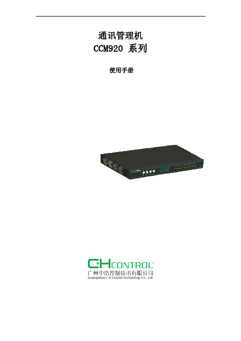
ccm920通讯管理机手册
目录
1. 概述...........................................................................................................................................4 1.1 功能及简介...............................................................................................................4 1.2 产品型号及含义.......................................................................................................5
下图为通讯管理机工程中使用时的结构图:
。
4
CCM920 系列通讯管理机采用 S3C2440 ARM920T 芯片,是新一代 32 位嵌入式智能通讯装 置。该产品低功耗,多串口,多以太网口的特点,特别适用于通讯规约转换、数据集中采集 和处理。支持多种通讯规约,实现各种微机保护、自动化装置、测控装置、智能化仪表、变 电站智能辅助设备和主计算机系统间的信息传递、合成、编辑、管理和设备监控功能。
5.2 参数编辑.................................................................................................................13 5.2.1 新建工程.........................................................................................................13 5.2.2 创建通道.........................................................................................................15 5.2.3 通道内添加装置.............................................................................................15 5.2.4 装置点表导入.................................................................................................17 5.2.5 通信机通道参数设置.....................................................................................20 5.2.6 通信机装置参数设置.....................................................................................22 5.2.7 转发表配置.....................................................................................................24 5.2.8 遥控点表配置.................................................................................................25 5.2.9 通信机参数导出.............................................................................................26
ARM入门教程.pdf

目录第1章 ARM微处理器概述 51.1 ARM-Advanced RISC Machines 51.2 ARM微处理器的应用领域及特点 51.2.1 ARM微处理器的应用领域 51.2.2 ARM微处理器的特点 61.3 ARM微处理器系列 61.3.1 ARM7微处理器系列 61.3.2 ARM9微处理器系列 71.3.3 ARM9E微处理器系列 71.3.4 ARM10E微处理器系列 71.3.5 SecurCore微处理器系列 81.3.6 StrongARM微处理器系列 81.3.7 Xscale处理器 81.4 ARM微处理器结构 81.4.1 RISC体系结构 81.4.2 ARM微处理器的寄存器结构 91.4.3 ARM微处理器的指令结构 91.5 ARM微处理器的应用选型 101.6 本章小节10第2章 ARM微处理器的编程模型 112.1 ARM微处理器的工作状态 112.2 ARM体系结构的存储器格式 112.3 指令长度及数据类型 122.4 处理器模式 122.5 寄存器组织 132.5.1 ARM状态下的寄存器组织 132.5.2 Thumb状态下的寄存器组织 152.5.3 程序状态寄存器 162.6 异常(Exceptions) 182.6.1 ARM体系结构所支持的异常类型 182.6.2 对异常的响应 182.6.3 从异常返回 192.6.4 各类异常的具体描述 192.6.5 异常进入/退出小节 202.6.6 异常向量(Exception Vectors) 202.6.7 异常优先级(Exception Priorities) 212.6.8 应用程序中的异常处理 212.7 本章小节21第3章 ARM微处理器的指令系统 223.1 ARM微处理器的指令集概述 223.1.1 ARM微处理器的指令的分类与格式 223.1.2 指令的条件域 233.2 ARM指令的寻址方式 233.2.1 立即寻址 243.2.2 寄存器寻址 243.2.2 寄存器间接寻址 243.2.3 基址变址寻址 243.2.4 多寄存器寻址 253.2.5 相对寻址 253.2.6 堆栈寻址 253.3 ARM指令集 253.3.1 跳转指令 253.3.2 数据处理指令 263.3.3 乘法指令与乘加指令 303.3.4 程序状态寄存器访问指令 323.3.5 加载/存储指令 323.3.6 批量数据加载/存储指令 343.3.7 数据交换指令 353.3.8 移位指令(操作) 353.3.9 协处理器指令 363.3.10 异常产生指令 383.4 Thumb指令及应用 383.5 本章小节39第4章 ARM程序设计基础 404.1 ARM汇编器所支持的伪指令 404.1.1 符号定义(Symbol Definition)伪指令 404.1.2 数据定义(Data Definition)伪指令 414.1.3 汇编控制(Assembly Control)伪指令 434.1.4 其他常用的伪指令 454.2 汇编语言的语句格式 484.2.1 在汇编语言程序中常用的符号 494.2.2 汇编语言程序中的表达式和运算符 494.3 汇编语言的程序结构 524.3.1 汇编语言的程序结构 524.3.2 汇编语言的子程序调用 524.3.3 汇编语言程序示例 534.3.4 汇编语言与C/C++的混合编程 554.4 本章小节56第5章应用系统设计与调试 575.1 系统设计概述 575.2 S3C4510B概述 585.2.1 S3C4510B及片内外围简介 585.2.2 S3C4510B的引脚分布及信号描述 615.2.3 CPU内核概述及特殊功能寄存器(Special Registers) 675.2.4 S3C4510B的系统管理器(System Manager) 725.3 系统的硬件选型与单元电路设计 825.3.1 S3C4510B芯片及引脚分析 825.3.2 电源电路 835.3.3 晶振电路与复位电路 835.3.4 Flash存储器接口电路 855.3.5 SDRAM接口电路 895.3.6 串行接口电路 935.3.7 IIC接口电路 945.3.8 JTAG接口电路 955.3.9 10M/100M以太网接口电路 965.3.10 通用I/O接口电路 1005.4 硬件系统的调试 1015.4.1 电源、晶振及复位电路 1015.4.2 S3C4510B及JTAG接口电路 1025.4.3 SDRAM接口电路的调试 1035.4.4 Flash接口电路的调试 1055.4.5 10M/100M以太网接口电路 1055.5 印刷电路板的设计注意事项 1055.5.1 电源质量与分配 1055.5.2 同类型信号线的分布 1065.6 本章小节 106 第6章部件工作原理与编程示例 1076.1 嵌入式系统的程序设计方法 1076.2 部件工作原理与编程示例 1086.2.1 通用I/O口工作原理与编程示例 1086.2.2 串行通讯工作原理与编程示例 1116.2.3 中断控制器工作原理与编程示例 1206.2.4 定时器工作原理与编程示例 1236.2.5 GDMA工作原理与编程示例 1276.2.6 IIC总线控制器工作原理 1336.2.7 以太网控制器工作原理 138主要特性139MAC功能模块 140 带缓冲DMA接口(Buffered DMA Interface) 144以太网控制器特殊功能寄存器(Ethernet Controller Special Registers) 147MAC寄存器(Media Access Control(MAC)Register) 154以太网控制器的操作(Ethernet Controller Operation) 160发送一个帧(Transmitting a Frame) 162接收一个帧(Receiving a Frame) 1626.2.8 Flash存储器工作原理与编程示例 1626.3 BootLoader简介 1676.4 本章小节 167 第7章嵌入式uClinux及其应用开发 1687.1 嵌入式uClinux系统概况 1687.2 开发工具GNU的使用 1707.2.1 GCC编译器 1707.2.2 GNU Make 1727.2.3 使用GDB调试程序 1777.3 建立uClinux开发环境 1807.3.1 建立交叉编译器 1817.3.2 uClinux针对硬件的改动 1847.3.3 编译uClinux内核 1857.3.4 内核的加载运行 1877.4 在uClinux下开发应用程序 1887.4.1 串行通信 1907.4.2 socket编程 1957.4 .3 添加用户应用程序到uClinux 2027.4.4 通过网络添加应用程序到目标系统 2057.5 本章小结 207 第8章ARM ADS集成开发环境的使用 2098.1 ADS集成开发环境组成介绍 2098.1.1 命令行开发工具 2098.1.2 ARM运行时库 2188.1.3 GUI开发环境(Code Warrior和AXD) 2198.1.4 实用程序 2218.1.5 支持的软件 2218.2 使用ADS创建工程 2228.2.1 建立一个工程 2228.2.2 编译和链接工程 2258.2.3 使用命令行工具编译应用程序 2298.3 用AXD进行代码调试 2308.4 本章小结 233第1章 ARM微处理器概述本章简介ARM微处理器的一些基本概念、应用领域及特点,引导读者进入ARM技术的殿堂。
ARMstep-U_v1.0.1

版权声明本手册版权归深圳市优龙科技有限公司所有,并保留一切权利。
非经作者本人同意(书面形式),任何单位和个人不可擅自抄录本手册或全部,以任何形式用于商业目的,但可以自由传播。
本产品所使用的嵌入式操作系统uClinux/Linux为开放源代码的自由软件,并遵循GNU通用公共许可协议GPL。
版权所有 Copyright©2006 深圳市优龙科技有限公司Copyright©2006 Shenzhen uCdragon Technology Co.,Ltd. All Rights ReservedARMstep-U使用手册第一章 ARMstep-U (3)1.1 ARMstep-U介绍 (3)1.2 套件清单 (4)1.3 Multi-ICE server软件使用详细介绍 (4)第二章 调试FS44b0XII(S3C44B0) (11)2.1 硬件连接 (11)2.2 设置AXD (12)2.3 从ADS进入调试环境 (15)第三章 调试FS2410(S3C2410) (19)3.1 硬件连接 (19)3.2 配置和使用 (19)第四章 调试YL2440(S3C2440) (28)4.1 硬件连接 (28)4.2 配置和使用 (28)第五章 调试YL9200(AT91RM9200) (34)5.1 硬件连接 (34)5.2 配置和使用 (34)第六章调试FS-PXA255(PXA255) (40)6.1 硬件连接 (40)6.2 配置和使用 (40)第七章 调试FS9315(EP9315) (45)7.1 硬件连接 (45)7.2 配置和使用 (45)附录一 软件的安装 (49)附录二 常见问题 (55)附录三 AXD高级使用 (57)第一章 ARMstep-U重要提示:本文档中的附录一、附录二、附录三为每个用户使用ARMstep仿真器前必读内容!!!1.1 ARMstep-U介绍优龙科技有限公司推出ARMstep-U仿真器(如下图所示)ARMstep-U仿真器是用ARM处理器调试的仿真器,符合IEEE 1149.1规范,并且与Multi-ICE兼容。
从零开始学arm9

从零开始学arm9引⾔快速⼊门HFRK2410开发板是基于三星公司S3C2410X ⾼性能ARM 处理器的嵌⼊开发平台,旨在为⽤户提供完整的嵌⼊式解决⽅案。
S3C2410由ARM920T 内核(16-/32-bit RISC CPU)、独⽴的16KB 指令和16KB 数据cache、MMU 虚拟内存管理单元、LCD 控制器(⽀持STN 和TFT)、NAND Flash bootloader、系统管理单元(SDRAM 控制器等)、3 通道UART、4 通道DMA、4 通道具备PWM 功能的定时器、IO ⼝、RTC(实时时钟)、8 通道10bit 精度ADC 和触摸屏控制器、IIC 总线接⼝、IIS 数字⾳频总线接⼝、USB 主机、USB 设备、SD/MMC 卡控制器、2 通道SPI 和PLL 数字锁相环组成。
HFRK2410嵌⼊开发平台是针对S3C2410的⼀款⾼性能开发平台,硬件软件都可根据⾃⼰的需求定制,具有⾼性能、低功耗、接⼝丰富等特点,因此你可以在此基础上开发⾃⼰的产品;⽽⼜因为开发板布局合理,接⼝排列整齐,适合直接按装使⽤,所以HFRK2410开发板同样也可以作为您的最终产品的⼀部分,可以直接把开发板整合到您的产品中。
第⼀节硬件概述HFRK2410硬件如下:CPU:采⽤SAMSUNG S3C2410 ARM920t CPU, 集成有串⼝,SD卡控制器,USB Host 和USB device控制器,LCD控制器, Nand Flash控制器等存储器:1. 64M SDRAM3. 64M Nand Flash ⽤于存放应⽤程序4. 32M Intel StrataFlash 32M(默认不焊接)5. SD卡⼀个VGA(直接连接普通PC显⽰器)、⼀个TFT输出接⼝(可以选购3.5⼨的夏普LCD)。
CS8900以太⽹控制器IDE接⼝,直接连接硬盘⼀个USB 主机接⼝⼀个USB 设备接⼝(可以切换成第⼆主机,需要更改驱动)⼀个总线扩展接⼝(包含16位数据,12位地址,两个⽚选,可以通过CPLD控制)。
- 1、下载文档前请自行甄别文档内容的完整性,平台不提供额外的编辑、内容补充、找答案等附加服务。
- 2、"仅部分预览"的文档,不可在线预览部分如存在完整性等问题,可反馈申请退款(可完整预览的文档不适用该条件!)。
- 3、如文档侵犯您的权益,请联系客服反馈,我们会尽快为您处理(人工客服工作时间:9:00-18:30)。
Product Overview ®ARM920TSystem-on-Chip Open OS ProcessorApplications •Applications running an Open OS:- Symbian OS- Linux, Palm OS- WindowsCE•High performance wireless applications:- Smart phones- PDAs•Networking applications •Digital set top boxes •Imaging•Automotive controlsolutions•Audio and video encoding and decodingBenefits•Designed specifically for System-on-Chipintegration•Supports the Thumbinstruction set offering thesame excellent codedensity as the ARM7TDMI •High performance allows system designers tointegrate more functionalityinto price andpower-sensitiveapplications demandingmore performance •Cached processor with an easy to use lowerfrequency on-chip systembus interface.The ARM920T™The ARM920T is a high-performance 32-bit RISC processor macrocell combining an ARM9TDMI™ processor core with:•16KB instruction and 16KB data caches•instruction and data Memory Management Units (MMUs)•write buffer•an AMBA™ (Advanced Microprocessor Bus Architecture) bus interface •an Embedded Trace Macrocell (ETM) interface.High performanceThe ARM920T provides a high-performance processor solution for open systems requiring full virtual memory management and sophisticated memory protection. An enhanced ARM® architecture v4 MMU implementation provides translation and access permission checks for instruction and data addresses. The ARM920T high-performance processor solution gives considerable savings in chip complexity and area, chip system design, and power consumption.Compatible with ARM7™ and StrongARM®The ARM920T processor is 100% user code binary compatible withARM7TDMI, and backwards compatible with the ARM7 Thumb® Family and the StrongARM processor families, giving designers software-compatible processors with a range of price/performance points from 60 MIPS to 200+ MIPS. Support for the ARM architecture today includes:•WindowsCE, Symbian OS, Linux, and QNX operating systems•40+ Real Time Operating Systems•co-simulation tools from leading EDA vendors•variety of software development tools.ARM920T MacrocellThe ARM920T macrocell is based on the ARM9TDMI Harvard architecture processor core, with an efficient 5-stage pipeline. The architecture of the processor core or integer unit is described in more detail page 9.To reduce the effect of main memory bandwidth and latency onperformance, the ARM920T includes:•instruction cache•data cache •MMU •TLBs •write buffer•physical address TAG RAM.CachesTwo 16KB caches are implemented, one for instructions, the other for data, both with an 8-word line size. A 32-bit data bus connects each cache to the ARM9TDMI core allowing a32-bit instruction to be fetched and fed into the instruction Decode stage of the pipeline at the same time as a 32-bit data access for the Memory stage of the pipeline.Cache lock-downCache lock-down is provided to allow critical code sequences to be locked into the cache to ensure predictability for real-time code. The cache replacement algorithm can beselected by the operating system asARM9TDMI Processor core(Integral EmbeddedICE)Write bufferIVA[31:0]DVA[31:0]External coprocessor interfaceeither pseudo random or round-robin. Both caches are 64-way set-associative. Lock-down operates on a per-set basis.Write bufferThe ARM920T also incorporates a 16-entry write buffer, to avoid stalling the processor when writes to external memory are performed.PATAG RAMThe ARM920T implements PAT AG RAM to perform write-backs from the data cache.The physical address of all the lines held in the data cache is stored by the P ATAG memory, removing the need for address translation when evicting a line from the cache. MMUsThe standard ARM920T implements an enhanced ARMv4 MMU to provide translation and access permission checks for the instruction and data address ports of theARM9TDMI.The MMU features are:•standard ARMv4 MMU mapping sizes, domains, and accessprotection scheme•mapping sizes are 1MB sections, 64KB large pages, 4KB smallpages, and new 1KB tiny pages •access permissions for sections •access permissions for large pages and small pages can bespecified separately for eachquarter of the page (thesequarters are called subpages)•16 domains implemented in hardware •64-entry instruction TLB and 64-entry data TLB•hardware page table walks •round-robin replacementalgorithm (also called cyclic).System controllerThe system controller oversees the interaction between the instruction and data caches and the Bus Interface Unit. It controls internal arbitration between the blocks and stalls appropriate blocks when required.The system controller arbitrates between instruction and data access to schedule single or simultaneous requests to the MMUs and the Bus Interface Unit. The system controller receives acknowledgement from each resource to allow execution to continue.Control coprocessor (CP15) The CP15 allows configuration of the caches, the write buffer, and other ARM920T options.Several registers within CP15 are available for program control, providing access to features such as:•invalidate whole TLB using CP15 •invalidate TLB entry, selected by modified virtual address, usingCP15•independent lock-down ofinstruction TLB and data TLBusing CP15 register 10•big or little-endian operation •low power state•memory partitioning andprotection•page table address•cache and TLB maintenance operations.RegistersThe ARM9TDMI processor core consists of a 32-bit datapath and associated control logic. This datapath contains 31 general-purpose registers, coupled to a full shifter, Arithmetic Logic Unit, and multiplier. At any one time 16 registers are visible to the user. The remainder are synonyms used to speed up exception processing. Register 15 is the Program Counter (PC) and can be used in all instructions to reference data relative to the current instruction. R14 holds the return address after a subroutine call. R13 is used (by software convention) as a stack pointer. Modes and exception handlingAll exceptions have banked registers for R14 and R13. After an exception, R14 holds the return address for exception processing. This address is used both to return after the exception is processed and to address the instruction that caused the exception.R13 is banked across exception modes to provide each exception handler with a private stack pointer. The fast interrupt mode also banks registers 8 to 12 so that interrupt processing can begin without the need to save or restore these registers.A seventh processing mode, System mode, does not have any banked registers. It uses the User mode registers. System mode runs tasks that require a privileged processor mode and allows them to invoke all classes of exceptions.Status registersAll other processor states are held instatus registers. The currentoperating processor status is in theCurrent Program Status Register(CPSR). The CPSR holds:•four ALU flags (Negative, Zero,Carry, and Overflow)• two interrupt disable bits (one foreach type of interrupt)• a bit to indicate ARM or Thumbexecution•and five bits to encode thecurrent processor mode.All five exception modes also have aSaved Program Status Register(SPSR) that holds the CPSR of thetask immediately before theexception occurred.Exception typesARM9TDMI supports five types ofexception, and a privilegedprocessing mode for each type. Thetypes of exceptions are:•fast interrupt (FIQ)•normal interrupt (IRQ)•memory aborts (used toimplement memory protection orvirtual memory)•attempted execution of anundefined instruction•software interrupts (SWIs).Conditional executionAll ARM instructions are conditionallyexecuted. Instructions optionallyupdate the four condition code flags(Negative, Zero, Carry, and Overflow)according to their result. Subsequentinstructions are conditionallyexecuted according to the status offlags. Fifteen conditions areimplemented.Four classes ofinstructionsThe ARM and Thumb instruction setscan be divided into four broadclasses of instruction:•data processing instructions•load and store instructions•branch instructions•coprocessor instructions.Data processingThe data processing instructionsoperate on data held in general-purpose registers. Of the two sourceoperands, one is always a register.The other has two basic forms:•an immediate value• a register value optionallyshifted.If the operand is a shifted register theshift amount might have animmediate value or the value ofanother register. Four types of shiftcan be specified. Most dataprocessing instructions can performa shift followed by a logical orarithmetic operation. Multiplyinstructions come in two classes:• normal, 32-bit result• long, 32-bit result variants.Both types of multiply instruction canoptionally perform an accumulateoperation.Load and storeThe second class of instruction is load and store instructions. These instructions come in two main types: •load or store the value of a single register•load and store multiple register values.Load and store single register instructions can transfer a 32-bit word, a 16-bit halfword and an 8-bit byte between memory and a register. Byte and halfword loads might be automatically zero extended or sign extended as they are loaded. Swap instructions perform an atomic load and store as a synchronization primitive.Addressing modesLoad and store instructions have three primary addressing modes:•offset•pre-indexed•post-indexed.They are formed by adding or subtracting an immediate or register- based offset to or from a base register. Register-based offsets can also be scaled with shift operations. Pre-indexed and post-indexed addressing modes update the base register with the base plus offset calculation. As the PC is a general-purpose register, a 32-bit value can be loaded directly into the PC to perform a jump to any address in the 4GB memory space.Block transfersLoad and store multiple instructions perform a block transfer of any number of the general purpose registers to or from memory. Four addressing modes are provided:•pre-increment addressing•post-increment addressing•pre-decrement addressing•post-decrement addressing.The base address is specified by aregister value (that can be optionallyupdated after the transfer). As thesubroutine return address and thePC values are in general-purposeregisters, very efficient subroutinecalls can be constructed.BranchAs well as allowing any dataprocessing or load instruction tochange control flow (by writing thePC) a standard branch instruction isprovided with 24-bit signed offset,allowing forward and backwardbranches of up to 32MB.Branch with LinkThere is a Branch with Link (BL) thatallows efficient subroutine calls. BLpreserves the address of theinstruction after the branch in R14(the Link Register or LR). This allowsa move instruction to put the LR in tothe PC and return to the instructionafter the branch.CoprocessorThere are three types of coprocessorinstructions:•coprocessor data processinginstructions invoke a coprocessorspecific internal operation•coprocessor register transferinstructions allow a coprocessorvalue to be transferred to or froman ARM register•coprocessor data transferinstructions transfer coprocessordata to or from memory, wherethe ARM calculates the addressof the transfer.The ARMv4T ARM instruction setMnemonic Operation Mnemonic OperationMOV Move MVN Move NotADD Add ADC Add with CarrySUB Subtract SBC Subtract with CarryRSB Reverse Subtract RSC Reverse Subtract with CarryCMP Compare CMN Compare NegatedEquivalence TST Test TEQ Test AND Logical AND BIC Bit ClearEOR Logical Exclusive OR ORR Logical (inclusive) ORMUL Multiply MLA Multiply AccumulateSMULL Sign Long Multiply SMLAL Signed Long Multiply Accumulate UMULL Unsigned Long Multiply UMLAL Unsigned Long Multiply Accumulate MRS Move From Status Register MSR Move to Status RegisterB BranchBL Branch and LinkBX Branch and Exchange SWI Software InterruptLDR Load Word STR Store WordLDRH Load Halfword STRH Store HalfwordLDRB Load Byte STRB Store ByteLDRSH Load Signed Halfword LDRSB Load Signed ByteLDMIA Load Multiple STMIA Store MultipleSWP Swap Word SWPB Swap ByteCDP Coprocessor Data ProcessingMRC Move From Coprocessor MCR Move to CoprocessorLDC Load To Coprocessor STC Store From CoprocessorThe ARMv4T Thumb instruction setMnemonic Operation Mnemonic OperationMOV Move MVN Move NotADD Add ADC Add with CarrySUB Subtract SBC Subtract with CarryRSB Reverse Subtract RSC Reverse Subtract with Carry CMP Compare CMN Compare NegatedTST Test NEG NegateAND Logical AND BIC Bit ClearEOR Logical Exclusive OR ORR Logical (inclusive) OR LSL Logical Shift Left LSR Logical Shift RightASR Arithmetic Shift Right ROR Rotate RightMUL MultiplyB Unconditional Branch Bcc Conditional BranchBL Branch and LinkBX Branch and Exchange SWI Software InterruptLDR Load Word STR Store WordLDRH Load Halfword STRH Store HalfwordLDRB Load Byte STRB Store ByteLDRSH Load Signed Halfword LDRSB Load Signed ByteLDMIA Load Multiple STMIA Store MultiplePUSH Push Registers to stack POP Pop Registers from stackModes and registersUser and System mode SupervisormodeAbort modeUndefinedmodeInterrupt modeFast InterruptmodeR0R0R0R0R0R0R1R1R1R1R1R1R2R2R2R2R2R2R3R3R3R3R3R3R4R4R4R4R4R4R5R5R5R5R5R5R6R6R6R6R6R6R7R7R7R7R7R7R8R8R8R8R8R8_FIQ R9R9R9R9R9R9_FIQ R10R10R10R10R10R10_FIQ R11R11R11R11R11R11_FIQ R12R12R12R12R12R12_FIQ R13R13_SVC R13_ABORT R13_UNDEF R13_IRQ R13_FIQ R14R14_SVC R14_ABORT R14_UNDEF R14_IRQ R14_FIQ PC PC PC PC PC PCCPSR CPSR CPSR CPSR CPSR CPSR SPSR_SVC SPSR_ABORT SPSR_UNDEF SPSR_IRQ SPSR_FIQMode-specific banked registersARM9TDMI processor coreThe ARM9TDMI processor core implements the ARMv4T Instruction Set Architecture (ISA). The ARMv4T ISA is a superset of the ARMv4 ISA (implemented by the StrongARM®processor) with additional support for Thumb instruction set (16-bit compressed ARM instruction set). The ARMv4T ISA is implemented by the ARM7™ Thumb family. This gives full upward compatibility to the ARM9™ Thumb family. Performance and code densityARM9TDMI executes two instruction sets: •32-bit ARM instruction set•16-bit Thumb instruction set.The ARM instruction set allows aprogram to achieve maximumperformance with the minimumnumber of instructions.The majority of ARM9TDMIinstructions are executed in a singlecycle. These are shown in theARM9TDMI instruction executiontiming table on page10.The simpler Thumb instruction setoffers much increased code densityincreasing space optimization. Codecan switch between the ARM andThumb instruction sets on anyprocedure call.ARM9TDMI integerpipeline stagesThe integer pipeline consists of fivestages to maximize instructionthroughput on ARM9TDMI:F: FetchD: Decode and register readE: Execute shift and alu, oraddress calculate, ormultiplyM: Memory access and multiplyW: Write registerARM9TDMI integer pipelinePipeliningBy overlapping the various stages of execution, ARM9TDMI maximizes the clock rate achievable to execute each instruction. It delivers a throughput approaching one instruction per cycle.32-bit data busesARM9TDMI provides 32-bit data buses:•between the processor core and the instruction and data caches •between coprocessors and the processor core.This allows ARM9TDMI to achieve very high-performance on many code sequences, especially those that require data movement in parallel with data processing.Coprocessors and pipelines The ARM9TDMI coprocessor interface allows full independent processing in the ARM execution pipeline and supports up to16 independent coprocessors.Debug featuresThe ARM9TDMI processor core also incorporates a sophisticated debug unit to allow both software tasks and external debug hardware to perform hardware and software breakpoint, single stepping, register, and memory access. This functionality is made available to software as a coprocessor and is accessible from hardware via the JTAG port. Full- speed, real-time execution of the processor is maintained until a breakpoint is hit. At this point control is passed either to a software handler or to JTAG control.Table 1: ARM9TDMI instruction execution timing Instruction class Issue cycles Result delay Condition failed1NAALU instruction10ALU instruction with register shift20MOV PC, Rx3NAALU instruction dest = PC40MUL 1..7 1..7MSR (flags only)10MSR (mode change)3NAMRS10LDR 11LDR with shifted offset12STR1NALDM1Position in list + 1 STM 1 NASWP21CDP1NAMRC11MCR1NALDC1Number of words STC1NASystem Issues and Third Party SupportJTAG debugThe internal state of the ARM920T is examined through a JTAG-style serial interface. This allows instructions to be serially inserted into the pipeline of the core without using the external data bus. Therefore, when in debug state, a store-multiple (STM) can be inserted into the instruction pipeline. This exports the contents of the ARM9TDMI registers. This data can be serially shifted out without affecting the rest of the system.AMBA bus architecture The ARM9 Thumb Family processors are designed for use with the AMBA multi-master on-chip bus architecture. AMBA includes an Advanced System Bus (ASB) connecting processors and high-bandwidth peripherals and memory interfaces, and a low-power peripheral bus allowing a large number of low-bandwidth peripherals.The ARM920T ASB implementation provides a 32-bit address bus and a 32-bit data bus for high-bandwidth data transfers made possible by on-chip memory and modern SDRAM and RAMBUS memories. Everything you need ARM provides a wide range of products and services to support its processor families, including software development tools, development boards, models, applications software, training, andconsulting services.The ARM Architecture today enjoysbroad third party support. TheARM9 Thumb Family processorsstrong software compatibility withexisting ARM families ensures thatits users benefit immediately fromexisting support. ARM is workingwith its software, EDA, andsemiconductor partners to extendthis support to use new ARM9Family features.Current supportSupport for the ARM Architecturetoday includes:•ARM Developer Suite (ADS)and RealView Developer Suite(RDS)- Integrated developmentenvironment- C, C++, assembler, simulatorsand windowing source-leveldebugger- available on Windows95,WindowsNT, and Unix.- ARM Multi-ICE™ JTAGinterface- allows EmbeddedICEsoftware debug of ARMprocessor systems- integrates with the ADS.•ARMulator instruction-accuratesoftware simulator•Development boards•Design Simulation Modelsprovide signoff quality ASIC-simulation•Software toolkits available fromARM, Cygnus/GNU,Greenhills,JavaSoft, MetaWare, Microtec,and Windriver allowing softwaredevelopment in C, C++, Java,FORTRAN, Pascal, Ada, andassembler.•20+ Real Time OperatingSystems including:- Windriver VxWorks- Sun Microsystems Chorus- JavaOS- Microtec VRTX- JMI- Embedded System ProductsRTXC- Integrated Systems pSOS.•Major OS including:- Microsoft WindowsCE- Symbian OS- Palm OS- Linux•Application softwarecomponents:- speech and imagecompression- software modem- Chinese character inputnetwork protocols- Digital AC3 decode- MPEG3 encode and decode- MPEG4 decode and encode•Hardware/softwarecosimulation tools from leadingEDA Vendors.For more information, seeContacting ARMARM, Thumb, StrongARM, and ARM Powered are registered trademarks of ARM LimitedARM7, ARM9, ARM10, ARM7TDMI, ARM9E-S, ARM920T ARM926EJ-S, ARM9TDMI, EmbeddedICE, and AMBA are trademarks of ARM Limited All other brands or product names are the property of their respective owners.Neither the whole nor any part of the information contained in, or the product described in, this document may be adapted or reproduced in any material form except with the prior written permission of the copyright holder.The product described in this document is subject to continuous developments and improvements. All particulars of the product and its use contained in this document are given by ARM Limited in good faith. However, all warranties implied or expressed, including but not limited to implied warranties or merchantability, or fitness for purpose, are excluded.This document is intended only to assist the reader in the use of the product. ARM Limited shall not be liable for any loss or damage arising from the use of any information in this document, or any error or omission in such information, or any incorrect use of the product.ARM, INC.750 University Avenue, Suite 150,Los Gatos CA 95032USATel: +1 408 579 2200Fax:+1 408 579 12051250 Capital of Texas Highway Building 3, Suite 560Austin, Texas 78746USATel: +1 512 327 9249Fax:+1 512 314 1078300 West Main St.,Suite 215Northborough, MA 01532USATel: +1 508 351 1670Fax:+1 508 351 1668Walnut Creek Design Center 1981 N Broadway, Suite 245Walnut Creek, CA 94596USATel: +1 925 944 9690Fax: +1 925 944 9612ARM GermanyRennweg 3385435 Erding GermanyTel: +49 8122 89209-0 Fax:+49 8122 89209-49ARM Ltd.110 Fulbourn Road Cambridge, CB1 9NJ EnglandTel: +44 1223 400400Fax:+44 1223 400410New Spring House 231 Glossop Road Sheffield, S10 2GW EnglandTel: +44 114 282 8000Fax: +44 114 282 8001Belthorn HouseWalker Road, Guide,Blackburn, BB1 2QE EnglandTel: +44 1254 893900Fax: +44 1254 893901ARM Korea Limited Room 1115,Hyundai Building 9-4, Soonae-Dong Boondang-Ku,SungnamKyunggi-do 463-020South KoreaTel: +82 31 712 8234Fax: + 82 31 713 8225ARM France12, Avenue des Pr és Montigny le Bretonneux78059 Saint Quentin en Yvelines Cedex, FranceTel: +33 1 30 79 05 10Fax: +33 1 30 79 05 11Les Cardoulines B2Route des Doline Sophia Antipolis 06560 Valbonne FranceTel: +33 4 92 96 88 60Fax: +33 4 92 96 88 79ARM KKDaini-Ueno Building 8F 3-7-18 Shin-Y okohama Kohoku-ku, Y okohama-Shi Kanagawa 222-0033JapanTel: +81 45 477 5260Fax: +81 45 477 5261ARM Taiwan Limited 8F no 50Lane 10Kee Hu Road Nei HuTaipei (114)TaiwanTel: +886 2 2627 1681Fax: +886 2 2627 1682。