6引脚8位闪存单片机
89E516RD中文
5
e-mail: szks@
深圳市科赛科技开发有限公司 0755-83000297 13316986132
P3[5]
I
T1:定时器 1 外部输入
P3[6]
O
WR#:外部数据存储器写信号
P3[7]
O
RD#:外部数据存储器读信号
PSEN#
I/O
程序存储使能。是对外部程序的读选通脉冲,当执行内部程序
深圳市科赛科技开发有限公司 0755-83000297 13316986132
SST89E52RD2 / SST89E54RD2 / SST89E58RD2 /SST89E516RD2 SST89V52RD2 / SST89V54RD2 / SST89V58RD2 /SST89V516RD2
2
e-mail: szks@
深圳市科赛科技开发有限公司 0755-83000297 13316986132 1.0 功能方框图
3
e-mail: szks@
深圳市科赛科技开发有限公司 0755-83000297 13316986132 2.0 引脚定义图
ALE 脉冲将被忽略。ALE 可以通过置位 SFR 的 Auxlilary.0 禁
止,置位后 ALE 只能在执行 MOVX 指令时被激活。
P4[3:0]5
I/O
Port4:P4 是带内部上拉的 4 位双向 I/O 口。P4 的输出可以驱
单片机引脚功能介绍

单片机引脚功能介绍单片机(Microcontroller)是一种以单芯片为中心的微型计算机系统,它集成了中央处理器(CPU)、存储器(RAM、ROM)、外设接口与定时器等多种功能。
单片机通过引脚与外部世界交互,引脚功能的不同决定了单片机在电路设计和应用中的具体用途。
以下是一些常见的单片机引脚功能介绍。
1.电源引脚:单片机需要供电才能正常工作,一般包括Vcc(5V或3.3V电源输入)、GND(电源地)和可能的电源滤波引脚。
2.输入/输出引脚(I/O):I/O 引脚用于连接单片机与外部电路或其他器件进行数据传输。
它可以用作数字输入引脚(Input)或数字输出引脚(Output)。
3.模拟输入引脚(ADC):模拟-数字转换器(ADC)引脚允许单片机测量外部模拟信号的大小和幅度。
它通常用于从传感器等外部设备获取模拟输入信号。
4.模拟输出引脚(DAC):数字-模拟转换器(DAC)引脚允许从单片机输出模拟信号,将数字数据转换为可变的模拟电压或电流信号。
这种信号通常用于控制执行器或其他模拟电路。
5. 定时器/计数器引脚(Timer/Counter):定时器和计数器引脚用于在特定时间间隔内生成脉冲信号、计数外部事件的脉冲数、测量时间等。
6. 中断引脚(Interrupt):中断引脚允许外部触发中断事件,使单片机停止正在执行的任务,并执行特定的中断处理程序。
这可以提高单片机对外部事件的响应速度。
单片机用串行通信引脚与其他设备进行数据交换。
常见的串行通信协议包括UART、SPI和I2C等。
8. 时钟引脚(Clock):时钟引脚用于提供单片机的时钟信号,以便同步单片机内部操作。
时钟信号的频率决定了单片机的工作速度。
9.外部存储器引脚:单片机可以与外部存储器(如闪存、EEPROM等)进行连接,以扩大其内部存储容量。
10.外部复位引脚:复位引脚用于将单片机复位到初始状态,使其重新启动。
这通常是通过将复位引脚与电源引脚连接或通过外部复位电路实现的。
Microchip超低功耗(XLP)系列新增高密度8位单片机
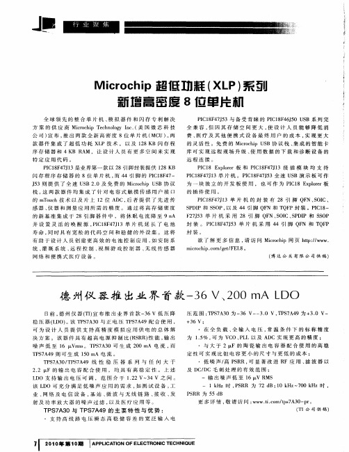
封 装 。 PC 8 4J3单 片 机 采 用 4 引 脚 Q N 和 T F I 1F 75 4 F QP
封装。
欲 了 解 更 多 信 息 , 访 问 Mi ohp网 页 ht : w w. 请 c ci r t / w p /
公 司 ) 布 , 出 两 款 全 新 高 密 度 8位 单 片 机 ( U ) 两 宣 推 MC 。
PC1 F 75 I 8 4 J 3与 备 受 青 睐 的 PC1 F 6 5 S 系 列 完 I 8 4 J0 U B 全 兼 容 , 因 其 存 储 空 间 更 大 , 设 计 人 员 能 够 降 低 消 但 使 费 、 疗 及 其 他 便 携 式 设 备 最 终 用 户 的 成 本 , 现 更 大 医 实 的灵 活 性 。免 费 的 Mirc i B 协 议 栈 、 成 的 智 能 卡 cohp US 集 库 可 实 现 远 程 现 场 升 级 、 用 数 据 的 下 载 和 诊 断 设 备 的 使
稳 压 器 (DO 。该 T S A 0与 正 电 压 T S A 9 配 合 使 用 , L ) P7 3 P7 4 压 范 围 : P 7 0 为 一 6 V—一 . , P 7 4 T S A3 3 30 V T S A 9为 + . 3 0 V~
十3 ; 6V
・
可 为 设 计 人 员 提 供 支 持 高 精 度 模 拟 应 用 供 电 的 总 体 解 决 方 案 。该 器 件 具 有 超 高 电 源 抑 制 比( S R) 能 , 出 RR 性 输
远 程连 接 。 PC1 E poe I 8 x lrr板 和 P C 8 4 J3 接 插 模 块 均 支 持 I1F 71
MCV14A中文说明书

初稿
2007 Microchip Technology Inc.
MCV14A
14 引脚 8 位闪存单片机
高性能 RISC CPU:
• 仅需学习 33 条单字指令 • 除了程序转移指令,所有指令都是单周期指令;程
序转移指令是双周期指令
• 2 层深硬件堆栈 • 数据和指令采用直接、间接和相对寻址模式 • 工作速度:
本出版物中所述的器件应用信息及其他类似内容仅为您提供便 利,它们可能由更新之信息所替代。确保应用符合技术规范, 是您自身应负的责任。Microchip 对这些信息不作任何明示或 暗示、书面或口头、法定或其他形式的声明或担保,包括但不 限于针对其使用情况、质量、性能、适销性或特定用途的适用 性的声明或担保。 Microchip 对因这些信息及使用这些信息而 引起的后果不承担任何责任。如果将 Microchip 器件用于生命 维持和 / 或生命安全应用,一切风险由买方自负。买方同意在 由此引发任何一切伤害、索赔、诉讼或费用时,会维护和保障 Microchip 免于承担法律责任,并加以赔偿。在 Microchip 知识 产权保护下,不得暗中或以其他方式转让任何许可证。
SQTP 是 Microchip Technology Inc. 在美国的服务标记。
在此提及的所有其他商标均为各持有公司所有。
© 2007, Microchip Technology Inc. 版权所有。
DS41338A_CN 第 ii 页
Microchip 位于美国亚利桑那州 Chandler 和 Tempe 与位于俄勒冈州 Gresham 的全球总部、设计和晶圆生产厂及位于美国加利福尼亚州和 印度的设计中心均通过了 ISO/TS-16949:2002 认证。公司在 PIC® MCU 与 dsPIC® DSC、 KEELOQ® 跳码器件、串行 EEPROM、单片机外 设、非易失性存储器和模拟产品方面的质量体系流程均符合 ISO/TS16949:2002。此外, Microchip 在开发系统的设计和生产方面的质量体 系也已通过了 ISO 9001:2000 认证。
单片机外文翻译--8位8字节闪存单片机AT89C52
电子与信息工程学院本科毕业论文(设计)外文文献翻译译文题目: 8-bit Microcontroller With 8K Bytes Flash AT89C52 学生姓名:专业:电气工程及其自动化指导教师:2012年11月外文资料8-bit Microcontroller With 8K Bytes Flash AT89C52FeaturesCompatible with MCS-51™ Products8K Bytes of In-System Reprogrammable Flash MemoryEndurance: 1,000 Write/Erase CyclesFully Static Operation: 0 Hz to 24 MHzThree-level Program Memory Lock256 x 8-bit Internal RAM32 Programmable I/O LinesThree 16-bit Timer/CountersEight Interrupt SourcesProgrammable Serial ChannelLow-power Idle and Power-down ModesDescriptionThe AT89C52 is a low-power, high-performance CMOS 8-bit microcomputer with 8K bytes of Flash programmable and erasable read only memory (PEROM). The device is manufactured using Atmel’s high-density nonvolatile memory technology and is compatible with the industry-standard 80C51 and 80C52 instruction set and pin out. The on-chip Flash allows the program memory to be reprogrammed in-system or by a conventional nonvolatile memory programmer. By combining a versatile 8-bit CPU with Flash on a monolithic chip, the Atmel AT89C52 is a powerful microcomputer which provides a highly-flexible and cost-effective solution to many embedded control applications.Pin ConfigurationsBlock DiagramPin DescriptionVCCSupply voltage.GNDGround.Port 0Port 0 is an 8-bit open drain bi-directional I/O port. As an output port, each pin can sink eight TTL inputs. When 1s are written to port 0 pins, the pins can be used as high-impedance inputs. Port 0 can also be configured to be the multiplexed low-order address/data bus during accesses to external program and data memory. In this mode, P0 has internal pull-ups. Port 0 also receives the code bytes during Flash programming and outputs the code bytes during program verification. External pull-ups are required during program verification.Port 1Port 1 is an 8-bit bi-directional I/O port with internal pull-ups. The Port 1 output buffers can sink/source four TTL inputs. When 1s are written to Port 1 pins, they are pulled high by the internal pull-ups and can be used as inputs. As inputs, Port 1 pins that are externally being pulled low will source current (I IL) because of the internal pull-ups. In addition, P1.0 and P1.1 can be configured to be the timer/counter 2 external count input (P1.0/T2) and the timer/counter 2 trigger input (P1.1/T2EX), respectively, as shown in the following table. Port 1 also receives the low-order address bytes during Flash programming and verification.Port 2Port 2 is an 8-bit bi-directional I/O port with internal pull-ups. The Port 2 outputbuffers can sink/source four TTL inputs. When 1s are written to Port 2 pins, they are pulled high by the internal pull-ups and can be used as inputs. As inputs, Port 2 pins that are externally being pulled low will source current (I IL) because of the internal pull-ups. Port 2 emits the high-order address byte during fetches from external program memory and during accesses to external data memories that use 16-bit addresses (MOVX @DPTR). In this application, Port 2 uses strong internal pull-ups when emitting 1s. During accesses to external data memories that use 8-bit addresses (MOVX @ RI), Port 2 emits the contents of the P2 Special Function Register. Port 2 also receives the high-order address bits and some control signals during Flash programming and verification.Port 3Port 3 is an 8-bit bi-directional I/O port with internal pull-ups. The Port 3 output buffers can sink/source four TTL inputs. When 1s are written to Port 3 pins, they are pulled high by the internal pull-ups and can be used as inputs. As inputs, Port 3 pins that are externally being pulled low will source current (I IL) because of the pull-ups. Port 3 also serves the functions of various special features of the AT89C51, as shown in the following table. Port 3 also receives some control signals for Flash programming and verification.RSTReset input. A high on this pin for two machine cycles while the oscillator is running resets the device.ALE/PROGAddress Latch Enable is an output pulse for latching the low byte of the address during accesses to external memory. This pin is also the program pulse input (PROG) during Flash programming. In normal operation, ALE is emitted at a constant rate of 1/6 the oscillator frequency and may be used for external timing or clocking purposes. Note, however, that one ALE pulse is skipped during each access to external data memory. If desired, ALE operation can be disabled by setting bit 0 of SFR location 8EH. With the bit set, ALE is active only during a MOVX or MOVC instruction. Otherwise, the pin is weakly pulled high. Setting the ALE-disable bit has no effect if the microcontroller is in external execution mode.PSENProgram Store Enable is the read strobe to external program memory. When the AT89C52 is executing code from external program memory, PSEN is activated twice each machine cycle, except that two PSEN activations are skipped during each access to external data memory.EA/VPPExternal Access Enable. EA must be strapped to GND in order to enable the device to fetch code from external program memory locations starting at 0000H up to FFFFH. Note, however, that if lock bit 1 is programmed, EA will be internally latched on reset. EA should be strapped to V CC for internal program executions. This pin also receives the 12-volt programming enable voltage (V PP) during Flash programming when 12-volt programming is selected.XTAL1Input to the inverting oscillator amplifier and input to the internal clock operating circuit.XTAL2Output from the inverting oscillator amplifier.Special Function RegistersA map of the on-chip memory area called the Special Function Register (SFR) space is shown in the Table 1.Note that not all of the addresses are occupied, and unoccupied addresses may not be implemented on the chip. Read accesses to these addresses will in general return random data, and write accesses will have an indeterminate effect. User software should not write 1s to these unlisted locations, since they may be used in future products to invoke new features. In that case, the reset or inactive values of the new bits will always be 0.Timer 2 RegistersControl and status bits are contained in registers T2CON and T2MOD for Timer 2. The register pair (RCAP2H, RCAP2L) are the Capture/Reload registers for Timer 2in 16-bit capture mode or 16-bit auto-reload mode.Interrupt RegistersThe individual interrupt enable bits are in the IE register. Two priorities can be set for each of the six interrupt sources in the IP register.Data MemoryThe AT89C52 implements 256 bytes of on-chip RAM. The upper 128 bytes occupy a parallel address space to the Special Function Registers. That means the upper 128 bytes have the same addresses as the SFR space but are physically separate from SFR space.When an instruction accesses an internal location above address 7FH, the address mode used in the instruction specifies whether the CPU accesses the upper 128 bytes of RAM or the SFR space. Instructions that use direct addressing access SFR space. For example, the following direct addressing instruction accesses the SFR at location 0A0H .MOV 0A0H, #dataInstructions that use indirect addressing access the upper 128 bytes of RAM. For example, the following indirect addressing instruction, where R0 contains 0A0H, accesses the data byte at address 0A0H, rather than P2 (whose address is 0A0H).MOV @R0, #dataNote that stack operations are examples of indirect addressing, so the upper 128 bytes of data RAM are available as stack space.Timer 0 and 1Timer 0 and Timer 1 in the AT89C52 operate the same way as Timer 0 and Timer 1 in the AT89C51.Timer 2 is a 16-bit Timer/Counter that can operate as either a timer or an event counter. The type of operation is selected by bit C/T2 in the SFR T2CON.Timer 2 has three operating modes: capture, auto-reload (up or down counting), and baud rate generator. The modes are selected by bits in T2CON, as shown in Table 3.Timer 2 consists of two 8-bit registers, TH2 and TL2. In the Timer function, the TL2 register is incremented every machine cycle. Since a machine cycle consists of 12 oscillator periods, the count rate is 1/12 of the oscillator frequency.In the Counter function, the register is incremented in response to a 1-to-0 transition at its corresponding external input pin, T2. In this function, the external input is sampled during S5P2 of every machine cycle. When the samples show a high in one cycle and a low in the next cycle, the count is incremented. The new count value appears in the register during S3P1 of the cycle following the one in which the transition was detected. Since two machine cycles (24 oscillator periods) are required to recognize a 1-to-0 transition, the maximum count rate is 1/24 of the oscillator frequency. To ensure that a given level is sampled at least once before it changes, the level should be held for at least one full machine cycle.Capture ModeIn the capture mode, two options are selected by bit EXEN2 in T2CON. If EXEN2 = 0, Timer 2 is a 16-bit timer or counter which upon overflow sets bit TF2 in T2CON.This bit can then be used to generate an interrupt. If EXEN2 = 1, Timer 2 performs the same operation, but a 1-to-0 transition at external input T2EX also causes the current value in TH2 and TL2 to be captured into RCAP2H and RCAP2L, respectively. In addition, the transition at T2EX causes bit EXF2 in T2CON to be set. The EXF2 bit, like TF2 can generate an interrupt. The capture mode is illustrated inAuto-reload (Up or Down Counter)Timer 2 can be programmed to count up or down when configured in its 16-bit auto-reload mode. This feature is invoked by the DCEN (Down Counter Enable) bit located in the SFR T2MOD. Upon reset, the DCEN bit is set to 0 so that timer 2 will default to count up. When DCEN is set, Timer 2 can count up or down, depending on the value of the T2EX pin.Figure 2 shows Timer 2 automatically counting up when DCEN = 0. In this mode, two options are selected by bit EXEN2 in T2CON. If EXEN2 = 0, Timer 2 counts up to 0FFFFH and then sets the TF2 bit upon overflow. The overflow also causes the timer registers to be reloaded with the 16-bit value in RCAP2H and RCAP2L. The values in Timer in Capture ModeRCAP2H and RCAP2L are preset by software. If EXEN2 = 1, a 16-bit reload can be triggered either by an overflow or by a 1-to-0 transition at external input T2EX. This transition also sets the EXF2 bit. Both the TF2 and EXF2 bits can generate an interrupt if enabled.Setting the DCEN bit enables Timer 2 to count up or down, as shown in Figure 3. In this mode, the T2EX pin controls the direction of the count. A logic 1 at T2EX makes Timer 2 count up. The timer will overflow at 0FFFFH and set the TF2 bit. This overflow also causes the 16-bit value in RCAP2H and RCAP2L to be reloaded into the timer registers, TH2 and TL2, respectively.A logic 0 at T2EX makes Timer 2 count down. The timer underflows when TH2 and TL2 equal the values stored in RCAP2H and RCAP2L. The underflow sets the TF2 bit and causes 0FFFFH to be reloaded into the timer registers. The EXF2 bit toggles whenever Timer 2 overflows or underflows and can be used as a 17th bit of resolution. In this operating mode, EXF2 does not flag an interrupt.外文资料译文:8位8字节闪存单片机AT89C52主要性能●与MCS-51单片机产品兼容●8K字节在系统可编程Flash存储器●1000次擦写周期●全静态操作:0Hz~24Hz●三级加密程序存储器●256×8位内部存储器●32个可编程I/O口线●三个16位定时器/计数器●八个中断源●可编程串行通道●低功耗空闲和掉电模式功能特性描述AT89S52是一种低功耗、高性能CMOS8位微控制器,具有8K内置可编程闪存。
飞思卡尔8位单片机—飞思卡尔8位单片机基础知识

7〉 管脚的复用
注意: 0、管脚功能复用时的优先 级见右表,高优先级接管管 脚时,对低优先级模块会产 生杂乱信号,因此切换前应 先停止不使用的功能。 1、PTA5作为只能输入管脚 而言,输入电压不能超过 VDD。 2、IIC使用的端口可以通过 设置SOPT2 寄存器中的 IICPS位重新定位到PTB6和 PTB7,复位时缺省使用 PTA2 and PTA3。 3、如果ACMP和ADC被同 时使能,管脚PTA0和PTA1 可同时使用。
管脚及其功能
6〉 管脚控制寄存器
位于高页面的管脚控制寄存器,可以独立设置每个管 脚的输出驱动强度、输出信号变化速度、输入脚的内部 上拉允许等。内部上拉的设置有些时候自动失效,比如 管脚设为输出、管脚被外设使用、管脚作为模拟电路使 用等。如果管脚被用于键盘中断KBI模块,,并设置上升 沿触发,则允许上拉时实际是配置了下拉电阻。 对输出管脚设置了输出变化速度控制后,可以减少 EMC辐射,变化速度控制对输入脚无效。 输出管脚的输出驱动强度控制,可以选择更大的驱 动电流,虽然每个输出管脚都可以设置成大电流驱动, 但总电流不能超出芯片的工作范围。同时大驱动电流对 EMC辐射也会有一定影响。
• EPROM
EPROM(Erasable Programmable ROM,可擦除可编 程ROM)芯片可重复擦除和写入,。EPROM芯片在其正 面的陶瓷封装上,开有一个玻璃窗口,透过该窗口,可以 看到其内部的集成电路, 紫外线透过该孔照射内部芯片 就可以擦除其内的数据,完成芯片擦除的操作要用到 EPROM擦除器。EPROM内资料的写入要用专用的编程 器,并且往芯片中写 内容时必须要加一定的编程电压( VPP=12—24V,随不同的芯片型号而定)。EPROM的型 号是以27开头的,如27C020(8*256K)是一片 2M Bits容 量的EPROM芯片。EPROM芯片在写入资料后,还要以 不透光的贴纸或胶布把窗口封住,以免受到周围的紫外线 照射而使资料受损
单片机

1 系统硬件介绍本设计通过单片机实现喇叭播放音乐和LCD液晶显示文字、图片、动画,并通过键盘进行控制操作,实现功能的选择。
单片机使用AT89C55WD芯片,容有20K字节可编程闪烁存储器,能存放做够的程序容量。
LCD使用128*64液晶屏,通过控制驱动器,能显示图片和文字。
另外使用I2C总线扩展,I2C总线是一种用于IC器件之间连接的二线制总线。
它通过SDA(串行数据线)及SCL(串行时钟先)两根线在连到总线上的器件之间传送信息,并根据地址识别每个器件,不管是单片机、存储器、LCD驱动器还是键盘接口。
1.1 单片机简介所谓单片机,通俗的来讲,就是把中央处理器CPU(Central Processing Unit),存储器(memory),定时器,I/O(Input/Output)接口电路等一些计算机的主要功能部件集成在一块集成电路芯片上的微型计算机。
单片机又称为“微控制器MCU”。
中文“单片机”的称呼是由英文名称“Single Chip Microcomputer”直接翻译而来的。
顾名思义,这种计算机的最小系统只用了一片集成电路,即可进行简单运算和控制。
因为它体积小,通常都藏在被控机械的“肚子”里。
它在整个装置中,起着有如人类头脑的作用,它出了毛病,整个装置就瘫痪了。
现在,这种单片机的使用领域已十分广泛,如智能仪表、实时工控、通讯设备、导航系统、家用电器等。
各种产品一旦用上了单片机,就能起到使产品升级换代的功效,常在产品名称前冠以形容词——“智能微电脑型”,如智能型热水器等。
本设计用到的单片机是AT89C55WD,下面就以AT89C55WD为例,结合本设计所用到的内容,简单介绍一下单片机的基础知识。
1.1.1 AT89C55WD简介AT89C55WD是一个低电压,高性能CMOS 8 位单片机,片内含有20KB 的可重写快速闪存存储器和只读程序和256 bytes的随机存取数据存储器(RAM),器件采用ATMEL公司的高密度、非易失性存储技术生产,兼容标准MCS-51指令系统,引脚兼容工业标准芯片,采用通用编程方式,片内置通用8位中央处理器和Flash存储单元,内置功能强大的微处理器的AT89C55WD可为您提供许多高性价比的解决方案,适用于多数嵌入式应用系统。
51单片机引脚介绍(全)

51单片机引脚介绍(全)51单片机引脚介绍(全)单片机(Microcontroller)是一种集成了微处理器核心、存储器和各种输入输出控制电路的集成电路芯片,广泛应用于嵌入式系统中。
而51单片机(8051 Microcontroller)是最早被广泛使用的一款单片机型号,其引脚布局和功能十分重要。
本文将对51单片机的引脚进行详细介绍,以便更好地理解和应用。
1. 引脚简介51单片机共有40个引脚,编号为P0.0至P3.7,其中P0、P1、P2、P3为4个8位的I/O端口,分别对应于32个可编程的引脚。
此外,引脚还包括VCC(供电正极)、GND(接地)以及RESET(复位引脚)、PSEN(程序存储器使能引脚)、ALE/PROG(地址锁存/编程使能引脚)、EA/VPP(外部访问使能/编程电压),共计7个特殊功能引脚。
2. I/O口的功能P0口是可用的8位双向I/O口,可以用于与外设的数据传输。
P0口在模拟输入/输出工作状态下为双向I/O口,在数字输入/输出工作状态下为输出口。
P1口也是一个可用的8位双向I/O口,用于与外设的数据传输。
P2口是一个不可用的8位双向I/O口,它被用作外部总线的高8位数据总线。
P3口是一个可用的8位双向I/O口,用于与外设的数据传输。
3. 特殊功能引脚RESET引脚是用于复位单片机的引脚。
将RESET引脚拉低,即可使单片机复位。
PSEN引脚是用于访问外部程序存储器(EPROM或闪存)的引脚。
当PSEN为高时,表示访问的是程序存储器。
ALE/PROG引脚在T0(定时器0)的溢出和外部中断0激活时产生外部地址锁存信号。
在程序编程时,它与PSEN引脚一起用作编程使能信号,并提供编程电压。
EA/VPP引脚是用于控制单片机是否使用外部存储器。
当EA/VPP 为低时,表示单片机使用外部存储器;当EA/VPP为高时,表示单片机使用内部存储器。
4. 其他引脚VCC引脚是单片机的正电源引脚,需要接入正电源。
- 1、下载文档前请自行甄别文档内容的完整性,平台不提供额外的编辑、内容补充、找答案等附加服务。
- 2、"仅部分预览"的文档,不可在线预览部分如存在完整性等问题,可反馈申请退款(可完整预览的文档不适用该条件!)。
- 3、如文档侵犯您的权益,请联系客服反馈,我们会尽快为您处理(人工客服工作时间:9:00-18:30)。
6 引脚 8 位闪存单片机
2007 Microchip Technology Inc.
DS41239D_CN
请注意以下有关 Microchip 器件代码保护功能的要点: • Microchip 的产品均达到 Microchip 数据手册中所述的技术指标。
用的片上 RC 振荡器,以便可靠地工作
• 可编程代码保护 • 复用的 MCLR 输入引脚 • I/O 引脚可内部弱上拉
• 节能休眠模式 • 引脚电平变化时从休眠中唤醒
低功耗特性 /CMOS 技术:
• 工作电流: - < 175 µA @ 2V, 4 MHz,典型值
• 待机电流: - 100 nA @ 2V,典型值
4
8
GP3/MCLR/VPP
7
VSS
6
N/C
5
GP0/ICSPDAT/CIN+
8 引脚 DFN 引脚图
N/C VDD GP2/T0CKI/FOSC4 GP1/ICSPCLK
1
8
2
7
3
645ຫໍສະໝຸດ GP3/MCLR/VPP VSS N/C GP0/ICSPDAT
PIC10F200/202
N/C VDD GP2/T0CKI/COUT/FOSC4 GP1/ICSPCLK/CIN-
2007 Microchip Technology Inc.
PIC10F200/202/204/206
6 引脚 8 位闪存单片机
本数据手册针对下列器件:
• PIC10F200 • PIC10F202
• PIC10F204 • PIC10F206
高性能 RISC CPU:
• 仅有 33 条单字指令
8 引脚 PDIP 引脚图
N/C
1
VDD
2
GP2/T0CKI/FOSC4
3
GP1/ICSPCLK
4
8
GP3/MCLR/VPP
7
VSS
6
N/C
5
GP0/ICSPDAT
PIC10F200/202
PIC10F204/206
N/C
1
VDD
2
GP2/T0CKI/COUT/FOSC4
3
GP1/ICSPCLK/CIN-
GP0/ICSPDAT VSS
GP1/ICSPCLK
1
6
2
5
3
4
GP3/MCLR/VPP VDD GP2/T0CKI/FOSC4
PIC10F200/202
PIC10F204/206
GP0/ICSPDAT/CIN+ VSS
GP1/ICSPCLK/CIN-
1
6
2
5
3
4
GP3/MCLR/VPP VDD GP2/T0CKI/COUT/FOSC4
1
8
2
7
3
6
4
5
GP3/MCLR/VPP VSS N/C GP0/ICSPDAT/CIN+
PIC10F204/206
DS41239D_CN 第2页
2007 Microchip Technology Inc.
PIC10F200/202/204/206
目录
1.0 器件概述 ....................................................................................................................................................................................... 5 2.0 PIC10F200/202/204/206 器件种类 ............................................................................................................................................... 7 3.0 架构概述 ....................................................................................................................................................................................... 9 4.0 存储器构成 ................................................................................................................................................................................. 15 5.0 I/O 端口 ...................................................................................................................................................................................... 25 6.0 Timer0 模块和 TMR0 寄存器 (PIC10F200/202)...................................................................................................................... 29 7.0 Timer0 模块和 TMR0 寄存器 (PIC10F204/206)...................................................................................................................... 33 8.0 比较器模块 ................................................................................................................................................................................. 37 9.0 CPU 的特性 ................................................................................................................................................................................ 41 10.0 指令集汇总 ................................................................................................................................................................................. 51 11.0 开发支持 ..................................................................................................................................................................................... 59 12.0 电气特性 ..................................................................................................................................................................................... 63 13.0 DC 及 AC 特性图表 .................................................................................................................................................................... 73 14.0 封装信息 ..................................................................................................................................................................................... 81 索引 ..................................................................................................................................................................................................... 89 Microchip 网站...................................................................................................................................................................................... 91 变更通知客户服务 ................................................................................................................................................................................ 91 客户支持............................................................................................................................................................................................... 91 读者反馈表 ........................................................................................................................................................................................... 92 产品标识体系 ....................................................................................................................................................................................... 93