Adaptive Optimization for 3PAR Configure multiple tiers of storage devices for maximum performance
铁路通信传输与接入网工程设计规范

铁路通信传输及接入网工程设计规1总则1.0.1 为统一铁路通信传输及接入网工程的设计标准,提高工程设计质量,制定本规。
1.0.2 本规适用于新建、改建的铁路传输及接入网系统工程建设。
1.0.3 铁路通信传输及接入网工程设计应贯彻国家和铁路基本建设方针、政策,符合铁路运输生产和提高现代化管理水平的需要。
1.0.4 铁路通信传输及接入网工程建设应遵循技术先进、经济适用、安全可靠和统一标准(制式)、符合运输、合理布局、互联互通、资源共享的原则。
新建和改建的工程都应做好与既有铁路通信网的衔接,合理利用既有资源。
条文说明:铁路通信传输系统是一个全程全网的系统。
任何新建的通信传输系统都不会是一个孤立的系统,它总是要与其他网络(包括传输网络)互联,信息要进行交换。
因此,新建和改建的工程都应做好与既有铁路通信网的衔接,合理利用既有资源,这部分也是设计应重点关注和考虑的问题。
1.0.5 作为铁路通信各种业务的基础承载平台,铁路通信传输及接入网应结合通信技术发展的主流,向传输数字化、管理智能化、业务多样化发展。
1.0.6 铁路通信传输及接入网工程设计应与业务需求和发展规划相适应,以近期业务需求为主,兼顾远期业务发展。
机房等不易改、扩建的基础设施宜按远期设计,电源等宜按近期设计,系统其他设备可按交付运营后五年设计。
条文说明:铁路通信传输及接入网工程以设备为主,而且投资相对较大,因此不宜按照初期考虑,应适当考虑延长设备的使用寿命,但也要结合产品的更新换代速度,因此综合以上因素考虑,设计年度按照近期为宜。
通信机房、外电等不易扩容的基础设施宜按照远期考虑。
1.0.7 铁路通信传输及接入网工程设计除应符合本规外,尚应符合《铁路运输通信设计规》(TB 10006)和国家现行有关标准的相关规定。
2术语和符号2.1术语2.1.1 铁路通信 railway communication用于铁路运输组织、客货营销、经营管理等方面信息传输与交换的各种通信系统的总称。
NSR-300系列高压保护及平台介绍

NSR-300系列继电保护装置简介国电南瑞科技股份有限公司一装置整体平台介绍二线路保护及辅助保护三变压器保护四母差保护1.特高压建设、交直流系统互联,对继电保护适应性提出了新要求。
2.智能电网、智能变电站建设给继电保护提出了新课题。
智能一次设备、电子式互感器、数字化的二次回路及IEC61850标准的应用,使得保护装置的构成形式及继电保护系统的实施方案有了新的变化。
3. 日益复杂的电网结构与运行方式给继电保护提出了新问题和要求。
问题主要包括:☐同塔双回线跨线故障选相☐弱电强磁问题☐开关性能改善带来新的功率倒向问题☐励磁涌流与故障电流的识别☐纵联差动保护的光纤通道问题☐非故障相CT饱和对差动保护的影响......4. 研制目标:总结、抽取各种保护装置的共性需求,构建结构清晰、灵活通用、扩展能力强、可靠性高的软硬件平台。
研究解决当前存在问题的原理和方案。
在统一平台和成熟保护算法的基础上,进行了一定的技术创新,研制NSR-300系列保护装置,构成了涵盖35kV-1000kV电压等级,完整的高压、超高压系列成套保护装置。
NSR-302、NSR-303超高压线路保护装置NSR-371 母线保护装置NSR-376 发电机变压器组保护装置NSR-377 并联电抗器保护装置平台硬件平台软件数据通信总线通信管理板保护处理板输入输出板统一编程接口自检及监视调试、组态工具保护应用保护功能线路保护母差保护主变保护板卡间通信任务调度底层驱动与控制结构分层:按硬件、支撑软件、应用进行分层。
功能分块:每层按照功能模块划分。
灵活组合:根据不同的插件、不同的软件功能模块组建合适的应用装置。
充分解耦:⏹应用与硬件通过支撑软件隔离⏹支撑程序提供统一编程接口,应用与支撑程序独立。
优点:结构清晰、扩展性好、适应性强1. NSR-300系列装置平台构架ADCADCCPUFPGA以太网接口DSP继电器E/O E/O输出阵列滤波+E信号事件记录跳闸UIDC+DC-地串 口5V24V 0V0V 正常运行告警前面板指示灯打印机工厂调试口GPS键盘液晶监控系统监控系统保信子站调试网口SVGOOSE信号UI滤波测试仪2. NSR-300系列装置平台硬件构架2. NSR-300系列装置平台硬件构架➢装置的核心是一块CPU和一块DSP➢CPU系统负责总启动,只有总起动元件动作才能开放出口继电器正电源➢DSP负责保护功能,两者同时发出开出命令装置才会出口➢装置既支持常规互感器,也支持电子式互感器➢既支持继电器开出、光耦开入,也支持智能化接口➢ADC芯片选用8通道16位高精度并行同步采样ADC ➢CPU与DSP的数据采样系统(ADC)在电路上完全独立2. NSR-300系列装置平台硬件构架2. NSR-300系列装置平台硬件构架平台通过配置不同的板卡插件即可实现各种型号保护装置。
Adaptec SmartHBA 2200 Series:16i Tri-Mode SAS SATA
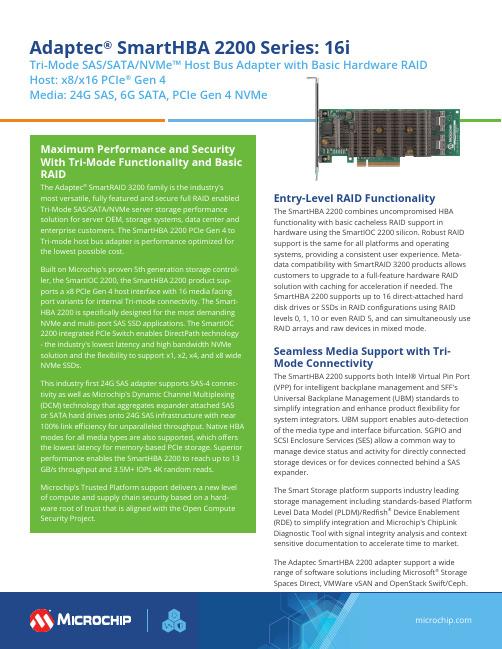
Adaptec® SmartHBA 2200 Series: 16iTri-Mode SAS/SATA/NVMe™ Host Bus Adapter with Basic Hardware RAID Host: x8/x16 PCIe® Gen 4Media: 24G SAS, 6G SATA, PCIe Gen 4 NVMeEntry-Level RAID FunctionalityThe SmartHBA 2200 combines uncompromised HBAfunctionality with basic cacheless RAID support inhardware using the SmartIOC 2200 silicon. Robust RAIDsupport is the same for all platforms and operatingsystems, providing a consistent user experience. Meta-data compatibility with SmartRAID 3200 products allowscustomers to upgrade to a full-feature hardware RAIDsolution with caching for acceleration if needed. TheSmartHBA 2200 supports up to 16 direct-attached harddisk drives or SSDs in RAID configurations using RAIDlevels 0, 1, 10 or even RAID 5, and can simultaneously useRAID arrays and raw devices in mixed mode.Seamless Media Support with Tri-Mode ConnectivityThe SmartHBA 2200 supports both Intel® Virtual Pin Port(VPP) for intelligent backplane management and SFF'sUniversal Backplane Management (UBM) standards tosimplify integration and enhance product flexibility forsystem integrators. UBM support enables auto-detectionof the media type and interface bifurcation. SGPIO andSCSI Enclo s ure Services (SES) allow a common way tomanage device status and activity for directly connectedstorage devices or for devices connected behind a SASexpander.The Smart Storage platform supports industry leadingstorage management including standards-based PlatformLevel Data Model (PLDM)/Redfish® Device Enablement(RDE) to simplify integration and Microchip's ChipLinkDiagnostic Tool with signal integrity analysis and contextsensitive documentation to accelerate time to market.The Adaptec SmartHBA 2200 adapter support a widerange of software solutions including Microsoft® StorageSpaces Direct, VMWare vSAN and OpenStack Swift/Ceph.The Microchip name and logo and the Microchip logo are registered trademarks of Microchip Technology Incorporated in the U.S.A. and other countries. All other trademarks mentioned herein are property of their respective companies. © 2023, Microchip Technology Incorporated and its subsidiaries. All Rights Reserved. 6/23 DS00003269DBenefits• Ideal for enabling PCIe Gen 4 storage capabilities for hyperscale applications, enterprise, and SMB, with proven reliability• Tri-mode support for SAS/SATA/NVMe devices• Combines full-featured, high-performance HBA functional-ity with basic hardware RAID• Built-in PCIe switch to enable ultra-low latency access to NVMe storage devices•Superior performance enabling up to 13 GB/s throughput and 3.5M+ IOPs 4K RRHighlights• Low profile, M D2 form factor• Fully tri-mode capable: 16 Gbps NVMe Gen 4, 24 Gbps SAS-4 and 6 Gbps SATA• 8-lane (x8) PCIe Gen 4 host interface• Internal SlimSAS connector (using SFF-9402 pinout to support U.2 and U.3)• Universal backplane management (UBM) • Virtual Pin Port Management (VPP)• SES (SAS expander-based backplanes), SGPIO (direct attached SAS/SATA backplanes)• Secure boot, secure update and attestation • Dynamic adapter power management • arcconf/maxView support• Support for 64 NVMe devices and up to 256 SAS/SATA devices • Broad inbox OS coverage• Comprehensive out-of-box driver support • Multi-initiator support •Support for x86 platform。
联想 ThinkServer SR590 V2 服务器产品指南

Lenovo ThinkServer SR590 V2 Server产品指南注:*此指南适用于ThinkServer SR590 V2 如下机型(机型号码7D53CTO1WW在服务器右耳标签,及机箱后侧标签中标注) **文档中涉及retimer 支持的功能将在2022年支持,如需了解详情,请联系联想相关销售人员联想ThinkServer SR590 V2是一款理想的2路2U机架服务器,它强劲性能和经济性的完美结合适用于中小型企业,大企业及各行业对于服务器的关键需求,如产品的高可靠性、易管理和高安全性,以及可扩展性及灵活性。
SR590 V2 基于新的第三代英特尔 Xeon 可扩展处理器系列(代号为"Icelake")并支持新的英特尔 Optane 持久内存200 系列。
SR590 V2 可以很好的支持各种工作负载,如数据库、虚拟化和云计算、虚拟桌面基础设施(VDI)、基础设施安全、系统管理、企业应用程序、协作/电子邮件、流媒体、Web 等ThinkServer SR590 V2 24盘位图关键产品信息SR590 V2 服务器搭载第三代英特尔 Xeon 可扩展处理器并能充分发会其的优异功能,可支持最高 205W 最多36 核处理器并发挥其完整性能、支持3200 MHz 内存以及对 PCIe Gen 4.0 支持。
同时SR590 V2 是一款支持丰富配置的产品,可最多支持服务器前置及后置共 28个硬盘,以及服务器后部最多8个PCIe 标准插槽及一个OCP 3.0 插槽,用以确保客户可以灵活配置服务器以满足其不同工作负载的需要。
Click here to check for updates主要特性SR590 V2 服务器结合了性能和灵活性及经济型的平衡,是各种规模的企业的绝佳选择。
该服务器提供广泛的硬盘驱动器和插槽配置的不同选择。
它的出色的可靠性、可用性和可维修性和优异的设计可改善客户的业务环境,并有助于节省运营成本。
SMT英文术语大全

BVT是Build Verification Test,基本验证测试,对完成的代码进行编译和连接,DVT是Design Verification Test的简称,设计验证测试,是硬件生产中不可缺少的一个检PVT全称为Process Verification Test,意为小批量过程验证测试,硬件测试的一种,主EVT-Engineer Verification Test,工程样品验证测试CPU: central processing unit(中央处理器)IC: Integrated circuit(集成电路)Memory IC: Memory Integrated circuit(记忆集成电路)RAM: Random Access Memory(随机存取存储器)DRAM: Dynamic Random Access Memory(动态随机存取存储器)SRAM: Staic Random Access Memory(静态随机存储器)ROM: Read-only Memory(只读存储器)EPROM:Electrical Programmable Read-only Memory(电可抹只读存诸器)EEPROM: Electrical Erasbale Programmable Read-only Memory(电可抹可编程只读存储CMOS: Complementary Metal-Oxide-Semiconductor(互补金属氧化物半导体)BIOS: Basic Input Output System(基本输入输出系统)Transistor:电晶体LED:发光二极体Resistor:电阻Variator:可变电阻Capacitor:电容Capacitor array:排容Diode:二极体Transistor:三极体Transformer:变压器(ADP)Oscillator:频率振荡器(0sc)Crystal:石英振荡器XTAL/OSC:振荡产生器(X)Relay:延时器Sensor:感应器Bead core:磁珠Filter:滤波器Flat Cable:排线Inductor:电感Buzzer:蜂鸣器Socket:插座Slot:插槽Fuse:熔断器Current:电流表Solder iron:电烙铁Magnifying glass:放大镜Caliper:游标卡尺Driver:螺丝起子Oven:烤箱TFT:液晶显示器Oscilloscope:示波器Connector:连接器PCB:printed circuit board(印刷电路板)PCBA: printed circuit board assembly(电路板成品)PP:并行接口HDD:硬盘FDD:软盘PSU:power supply unit(电源供应器)SPEC:规格Attach:附件Case: 机箱,盖子Cover:上盖Base:下盖Bazel:面板(panel)Bracket:支架,铁片Lable:贴纸Guide:手册Manual:手册,指南Card:网卡Switch:交换机Hub:集线器Router:路由器Sample:样品Gap:间隙Sponge:海绵Pallet:栈板Foam:保利龙Fiber:光纤Disk:磁盘片PROG:程序Barcode:条码System:系统System Barcode:系统条码M/B:mother board:主板CD-ROM:光驱FAN:风扇Cable:线材Audio:音效K/B:Keyboard(键盘)Mouse:鼠标Riser card:转接卡Card reader:读卡器Screw:螺丝Thermal pad:散热垫Heat sink:散热片Rubber:橡胶垫Rubber foot:脚垫Bag:袋子Washer:垫圈Sleeve:袖套Config:机构Label hi-pot:高压标签Firmware label:烧录标签Metal cover:金属盖子Plastic cover:塑胶盖子Tape for packing:包装带Bar code:条码Tray:托盘Collecto:集线夹Holder:固定器,L铁Connecter:连接器IDE:集成电路设备,智能磁盘设备SCSI:小型计算机系统接口Gasket:导电泡棉AGP:加速图形接口PCI:周边组件扩展接口LAN:局域网USB:通用串形总线架构Slim:小型化COM:串型通讯端口LPT:打印口,并行口Power cord:电源线I/O:输入,输出Speaker:扬声器EPE:泡棉Carton:纸箱Button:按键,按钮Foot stand:脚架部门名称的专有名词QS:Quality system品质系统CS:Coutomer Sevice 客户服务QC:Quality control品质管理IQC:Incoming quality control 进料检验LQC:Line Quality Control 生产线品质控制IPQC:In process quality control 制程检验FQC:Final quality control 最终检验OQC:Outgoing quality control 出货检验QA:Quality assurance 品质保证 SQA:Source(supplier) Quality Assurance 供应商品质保证(VQA) CQA:Customer Quality Assurance客户质量保证PQA rocess Quality Assurance 制程品质保证QE:Quality engineer 品质工程CE:component engineering零件工程EE:equipment engineering设备工程ME:manufacturing engineering制造工程TE:testing engineering测试工程PPE roduct Engineer 产品工程IE:Industrial engineer 工业工程ADM: Administration Department行政部RMA:客户退回维修CSDI:检修PC:producing control生管MC:mater control物管GAD: General Affairs Dept总务部A/D: Accountant /Finance Dept会计LAB: Laboratory实验室DOE:实验设计HR:人资PMC:企划RD:研发W/H:仓库SI:客验PD: Product Department生产部PA:采购(PUR: Purchaing Dept)SMT:Surface mount technology 表面粘着技术MFG:Manufacturing 制造MIS:Management information system 资迅管理系统DCC:document control center 文件管制中心厂内作业中的专有名词QT:Quality target品质目标QP:Quality policy目标方针QI:Quality improvement品质改善CRITICAL DEFECT:严重缺点(CR)MAJOR DEFECT:主要缺点(MA)MINOR DEFECT:次要缺点(MI)MAX:Maximum最大值MIN:Minimum最小值DIA iameter直径DIM imension尺寸LCL:Lower control limit管制下限UCL:Upper control limit管制上限EMI:电磁干扰ESD:静电防护EPA:静电保护区域ECN:工程变更ECO:Engineering change order工程改动要求(客户)ECR:工程变更需求单CPI:Continuous Process Improvement 连续工序改善Compatibility:兼容性Marking:标记DWG rawing图面Standardization:标准化Consensus:一致Code:代码ZD:Zero defect零缺点Tolerance:公差Subject matter:主要事项Auditor:审核员BOM:Bill of material物料清单Rework:重工ID:identification识别,鉴别,证明PILOT RUN: (试投产)FAI:首件检查FPIR:First Piece Inspection Report首件检查报告FAA:首件确认SPC:统计制程管制CP: capability index(准确度)CPK: capability index of process(制程能力) PMP:制程管理计划(生产管制计划)MPI:制程分析DAS efects Analysis System 缺陷分析系统PPB:十亿分之一Flux:助焊剂P/N:料号L/N:Lot Number批号Version:版本Quantity:数量Valid date:有效日期MIL-STD:Military-Standard军用标准ICT: In Circuit Test (线路测试)ATE:Automatic Test Equipment自动测试设备MO: Manafacture Order生产单T/U: Touch Up (锡面修补)I/N:手插件P/T:初测F/T: Function Test (功能测试-终测)AS 组立P/K:包装TQM:Total quality control全面品质管理MDA:manufacturing defect analysis制程不良分析(ICT) RUN-IN:老化实验HI-pot:高压测试FMI:Frequency Modulation Inspect高频测试DPPM: Defect Part Per Million(不良率的一种表达方式:百万分之一) 1000PPM即为0.1% Corrective Action: (CAR改善对策)ACC:允收REJ:拒收S/S:Sample size抽样检验样本大小SI-SIV:Special I-Special IV特殊抽样水平等级CON:Concession / Waive特采ISO:国际标准化组织ISA:Industry Standard Architecture工业标准体制结构OBA:开箱稽核FIFO:先进先出PDCA:管理循环Plan do check action计划,执行,检查,总结WIP:在制品(半成品)S/O: Sales Order (业务订单)P/O: Purchase Order (采购订单)P/R: Purchase Request (请购单)AQL:acceptable quality level允收品质水准LQL;Limiting quality level最低品质水准QVL:qualified vendor list合格供应商名册AVL :认可的供货商清单(Approved Vendor List) QCD: Quality cost delivery(品质,交期,成本)MPM:Manufacturing project management制造专案管理KPI:Key performance indicate重要绩效指标MVT:Manufacturing Verification Test制造验证试产Q/R/S:Quality/Reliability/Service质量/可靠度/服务STL:ship to line(料到上线)NTF:No trouble found误判CIP:capacity improvement plan(产能改善计划)MRB:material review board(物料审核小组)MRB:Material reject bill退货单JIT:just in time(即时管理)5S:seiri seiton seiso seiketsu shitsuke(整理,整顿,清扫,清洁,修养)SOP:standard operation process(标准作业程序)SIP:Specification inspection process制程检验规格TOP: Test Operation Process (测试作业流程)WI: working instruction(作业指导书)SMD:surface mounting device(表面粘着原件)FAR:failure aualysis report故障分析报告CAR:Corrective action report改善报告BPR: 企业流程再造 (Business Process Reengineering)ISAR :首批样品认可(Initial Sample Approval Request)-JIT:实时管理 (Just In Time)QCC :品管圈 (Quality Control Circle)Engineering Department (工程部)TQEM: Total Quality Environment Management(全面品质环境管理)PD: Production Department (制造)LOG: Logistics (后勤支持)Shipping: (进出口)AOQ:Average Output Quality平均出货质量AOQL:Average Output Quality Level平均出货质量水平FMEA:failure model effectiveness analysis失效模式分析CRB: Change Review Board (工程变更会议)CSA:Customer Simulate Analysis客户模拟分析SQMS:Supplier Quality Management System供应商品质管理系统QIT: Quality Improvement Team 品质改善小组QIP:Quality Improvement Plan品质改善计划CIP:Continual Improvement Plan持续改善计划M.Q.F.S: Material Quality Feedback Sheet (来料品质回馈单) SCAR: Supplier Corrective Action Report (供货商改善对策报告) 8D Sheet: 8 Disciplines sheet ( 8D单)PDCA:PDCA (Plan-Do-Check-Action) (管理循环)MPQ: Material Packing Quantity (物料最小包装量)DSCN: Delivery Schedule Change Notice (交期变更通知) QAPS: Quality Assurance Process Sheet (品质工程表)DRP :运销资源计划 (Distribution Resource Planning)DSS:决策支持系统 (Decision Support System)EC :电子商务 (Electronic Commerce)EDI :电子资料交换 (Electronic Data Interchange)EIS :主管决策系统 (Excutive Information System)ERP :企业资源规划 (Enterprise Resource Planning)FMS :弹性制造系统 (Flexible Manufacture System)KM :知识管理 (Knowledge Management)4L :逐批订购法 (Lot-for-Lot)LTC :最小总成本法 (Least Total Cost)LUC :最小单位成本 (Least Unit Cost)MES :制造执行系统 (Manufacturing Execution System)MPS :主生产排程 (Master Production Schedule)MRP :物料需求规划 (Material Requirement Planning)MRPⅡ:制造资源计划 (Manufacturing Resource Planning)OEM :委托代工 (Original Equipment Manufacture)ODM :委托设计与制造 (Original Design & Manufacture) OLAP:线上分析处理 (On-Line Analytical Processing)OLTP:线上交易处理 (On-Line Transaction Processing)OPT :最佳生产技术 (Optimized Production Technology) PDCA:PDCA管理循环 (Plan-Do-Check-Action)PDM:产品数据管理系统 (Product Data Management))RCCP:粗略产能规划 (Rough Cut Capacity Planning)SCM :供应链管理 (Supply Chain Management)SFC :现场控制 (Shop Floor Control)TOC:限制理论 (Theory of Constraints)TQC :全面品质管制 (Total Quality Control)FYI/R:for your information/reference仅供参考ASAP:尽快S/T:Standard time标准时间TPM:total production maintenance:全面生产保养ESD Wrist strap:静电环IT:information technology信息技术,资讯科学CEO:Chief Executive Officer执行总裁COO:Chief Operaring Officer首席业务总裁SWOT:Strength,Weakness,Opportunity,Threat优势﹐弱点﹐机会﹐威胁Competence:专业能力Communication:有效沟通Cooperation:统御融合Vibration Testing:振动测试IDP:Individual Development Plan个人发展计划MRP:Material Requirement Planning物料需求计划MAT'S:Material材料LRR:Lot Rejeet Rate批退率ATIN:Attention知会3C:Computer ,Communication , Consumer electronic消费性电子5W1H:When , Where , Who , What , Why , Ho5M: Man , Machine , Material , Method , Measurement人,机器,材料,方法,测量4MIE: Man,Material,Machine,Method,Environment人力,物力,财务,技术,时间(资源)7M1I: Manpower , Machine , Material , Method, Market , Management , Money , In 人力, 机器, 材料, 方法, 市场, 管理, 资金, 资讯1 Accuracy 准确度2 Action 行动3 Activity 活动4 Analysis Covariance 协方差分析5 Analysis of Variance 方差分析6 Approved 承认7 Attribute 计数值8 Average 平均数9 Balance sheet 资产负债对照表10 Binomial 二项分配11 Brainstorming Techniques 脑力风暴法12 Cause and Effect Matrix 因果图(鱼骨图)13 CL:Center Line 中心线14 Check Sheets 检查表15 Complaint 投诉16 Conformity 合格(符合)17 Control 控制18 Control chart 控制(管制)图19 Correction 纠正20 Correlation Methods 相关分析法21 CPI: continuouse Process Improvement 连续工序改善22 Cross Tabulation Tables 交叉表23 CS: Customer Sevice 客(户)服(务)中心24 DSA: Defects Analysis System 缺陷分析系统25 Data 数据 Description:品名26 DCC: Document Control Center 文控中心27 Decision 决策、判定28 Defects per unit 单位缺点数29 Description 描述30 Device 装置31 Do 执行32 DOE: Design of Experiments 实验设计33 Element 元素34 Engineering recbnology 工程技35 Environmental 环境36 Equipment 设备37 Estimated accumulative frequency 计算估计累计数38 E Equipment Variation 设备变异39 External Failure 外部失效,外部缺陷40 FA: Failure Analysis 失效分析41 Fact control 事实管理42 Fatigue 疲劳43 FMEA: Failure Mode and Effect Analysis失效模式与效果分析44 FP First-Pass Yield (第一次通过)合格率45 FQA: Final Quality Assurance 最终品质保证46 FQC: Final Quality control 最终品质控制47 Gauge system 测量系统48 Grade 等级49 Histogram 直方图50 Improvement 改善51 Initial review 先期审查52 Inspection 检验53 Internal Failure 内部失效、内部缺陷54 IPQC: In Process Quality Control 制程品质控制55 IQC: Incomming Quality Control 来料品质控制56 IS International Organization for Standardization 国际标准化组织57 LCL: Lower Control limit 管制下限58 LQC: Line Quality Control 生产线品质控制59 LSL: Lower Size Limit 规格下限60 Machine 机械61 Manage 管理62 Materials 物料63 Measurement 测量64 Median 中位数65 MSA: Measurement System Analysis 测量系统分析66 Occurrence 发生率67 Operation Instruction 作业指导书68 Organization 组织69 Parto 柏拉图70 PPM arts per Million (百万分之)不良率71 Plan 计划72 Policy 方针73 Population 群体74 PQA: Process Quality Assurance 制程品质保证75 Practice 实务(践)76 Prevention 预防77 Probability 机率78 Probability density function 机率密度函数79 Procedure 流程80 Process 过程81 Process capability analysis 制程能力分析(图)82 Process control and Process capability制程管制与制程能力83 Product 产品84 Production 生产85 Projects 项目86 QA: Quality Assurance 品质保证87 QC: Quality Control 品质控制88 QE: Quality Engineering 品质工程89 QFD: Quality Function Desgin 品质机能展开(法)90 Quality 质量91 Quality manual 品质手册92 Quality policy 品质政策(质量方针)93 Random experiment 随机试验94 Random numbers 随机数95 R:Range 全距(极差)96 Reject 拒收97 Repair 返修98 Repeatusility 再现性99 Reproducibility 再生性100 Requirement 要求101 Responsibilities 职责102 Review 评审103 Reword 返工104 Rolled yield 直通率105 RPN: Risk Priority Number 风险系数106 Sample 抽样,样本107 Sample space 样本空间108 Sampling with replacement 放回抽样109 Sampling without replacement 不放回抽样110 Scatter diagram 散布图分析111 Scrap 报废112 Simple random sampling 简单随机取样113 Size 规格114 SL: Size Line 规格中心线115 Stratified random sampling 分层随机抽样116 SOP: Standard Operation Procedure 标准作业书117 SPC: Statistical Process Control 统计制程管制118 Specification 规范119 SQA: Source(Supplier) Quality Assurance 供货商品质保证120 Stage sampling 分段随机抽样121 Standard Deviation 标准差122 Sum of squares 平方和123 Taguchi-method 田口(试验)方法124 Theory 原理125 TQC: Total Quality Control 全面品质控制126 TQM: Total Quality Management 全面品质管理127 Traceablity 追溯128 Training 培训129 UCL: Upper Control Limit 管制(控制)上限130 USL: Upper Size Limit 规格上限131 Validation 确认132 Variable 计量值133 Verification 验证134 Version 版本135 VOC: Voice of Customer 客户需求136 VOE: Voice of Engineer 工程需求137 Inventory stock report:庫存清单报告138 Sales order report:出货报告质量人员名称类QC quality control 品质管理人员FQC final quality control 终点质量管理人员IPQC in process quality control 制程中的质量管理人员OQC output quality control 最终出货质量管理人员IQC incoming quality control 进料质量管理人员TQC total quality control 全面质量管理POC passage quality control 段检人员QA quality assurance 质量保证人员OQA output quality assurance 出货质量保证人员QE quality engineering 质量工程人员质量保证类FAI first article inspection 新品首件检查FAA first article assurance 首件确认CP capability index 能力指数CPK capability process index 模具制程能力参数SSQA standardized supplier quality audit 合格供货商质量评估FMEA failure model effectiveness analysis 失效模式分析FQC运作类AQL Acceptable Quality Level 运作类允收质量水平S/S Sample size 抽样检验样本大小ACC Accept 允收REE Reject 拒收CR Critical 极严重的MAJ Major 主要的MIN Minor 轻微的Q/R/S Quality/Reliability/Service 质量/可靠度/服务P/N Part Number 料号L/N Lot Number 批号AOD Accept On Deviation 特采UAI Use As It 特采FPIR First Piece Inspection Report 首件检查报告PPM Percent Per Million 百万分之一制程统计品管专类SPC Statistical Process Control 统计制程管制SQC Statistical Quality Control 统计质量管理GRR Gauge Reproductiveness & Repeatability 量具之再制性及重测性判断量可靠与DIM Dimension 尺寸DIA Diameter 直径N Number 样品数其它质量术语类QIT Quality Improvement Team 质量改善小组ZD Zero Defect 零缺点QI Quality Improvement 质量改善QP Quality Policy 目标方针TQM Total Quality Management 全面质量管理RMA Return Material Audit 退料认可7QCTools 7 Quality Control Tools 品管七大手法通用之件类ECN Engineering Change Notice 工程变更通知(供货商) ECO Engineering Change Order 工程改动要求(客户)PCN Process Change Notice 工序改动通知PMP Product Management Plan 生产管制计划SIP Standard Inspection Procedure 制程检验标准程序SOP Standard Operation Procedure 制造作业规范IS Inspection Specification 成品检验规范BOM Bill Of Material 物料清单PS Package Specification 包装规范SPEC Specification 规格DWG Drawing 图面系统文件类ES Engineering Standard 工程标准CGOO China General PCE龙华厂文件IWS International Workman Standard 工艺标准ISO International Standard Organization 国际标准化组织GS General Specification 一般规格部类PMC Production & Material Control 生产和物料控制PCC Product control center 生产管制中心PPC Production Plan Control 生产计划控制MC Material Control 物料控制DC Document Center 资料中心QE Quality Engineering 质量工程(部)QA Quality Assurance 质量保证(处)QC Quality Control 质量管理(课)PD Product Department 生产部LAB Laboratory 实验室IE Industrial Engineering 工业工程R&D Research & Design 设计开发部生产类PCs Pieces 个(根,块等)PRS Pairs 双(对等)CTN Carton 卡通箱PAL Pallet/skid 栈板PO Purchasing Order 采购订单MO Manufacture Order 生产单D/C Date Code 生产日期码ID/C Identification Code (供货商)识别码SWR Special Work Request 特殊工作需求L/N Lot Number 批号P/N Part Number 料号OEM Original Equipment Manufacture 原设备制造PC Personal Computer 个人计算机CPU Central Processing Unit 中央处理器A.S.A.P As Soon As Possible 尽可能快的E-MAIL Electrical-Mail 电子邮件N/A Not Applicable 不适用QTY Quantity 数量I/O input/output 输入/输出NG Not Good 不行,不合格C=0 Critical=0 极严重不允许APP Approve 核准,认可,承认CHK Check 确认ASS'Y Assembly 装配,组装T/P True Position 真位度5WIH When, Where, Who, What, Why, How to6M Man, Machine, Material, Method, Measurement, Message4MTH Man, Material, Money, Method, Time, How 人力,物力,财务,技术,时间(资源SQA Strategy Quality Assurance 策略质量保证DQA Design Quality Assurance 设计质量保证MQA Manufacture Quality Assurance 制造质量保证SSQA Sales and service Quality Assurance 销售及服务质量保证LRR Lot Reject Rate 批退率SPS Switching power supply 电源箱DT Desk Top 卧式(机箱)MT Mini-Tower 立式(机箱)DVD Digital Video DiskVCD Video Compact DiskLCD Liquid Crystal DisplayCAD Computer Aided DesignCAM Computer Aided ManufacturingCAE Computer Aided EngineeringPCB Printed Circuit Board 印刷电路板CAR Correction Action Report 改善报告NG Not Good 不良WDR Weekly Delivery Requirement 周出货要求PPM Percent Per Million 百万分之一TPM Total Production Maintenance 全面生产保养MRP Material Requirement Planning 物料需计划OS Operation System 操作系统TBA To Be Assured 待定,定缺D/C Drawing ChangeP/P Plans & ProcedureEMI Electrical-Music Industry 电子音乐工业Electrical Magnetic Interference 电子干扰RFI Read Frequency Input 读频输入MMC Maximum Material ConditionMMS Maximum Material SizeLMC Least Material ConditionLMS Least Material SizeLED lighting-emitting diode 发光二极管QBR Quarter Business RecordCIP Continuous improvement processFGI Forecasted Goal InventoryCNC Computerized numeral controllerB2C Business to customerB2B Business to businessAVL Approved vendor listPOP Procedure of packagingEOL End of lifeVDCS Vender defect correcting sheet PDCS Process defect correcting sheet GRN Goods receiving noteA/R Accounting receivableA/P Accounting payable专业词汇通用类president董事长operator作业员position职务general manager总经理special assistant 特助deputy manager |'depjuti| =vice manager副理deputy supervisor =vice supervisor副课长group leader组长line leader线长supervisor 课长responsible department负责单位Human Resources Department人力资源部Head count 人头数production department生产部门planning department企划部QC Section品管课stamping factory冲压厂painting factory烤漆厂molding factory成型厂administration/general affairs dept./总务部production unit生产单位meeting minutes会议记录distribution department分发单位subject主题conclusion结论decision items决议事项pre-fixed finishing date预定完成日Color management 颜色管理Visual management 目视管理production capacity生产力first count初盘first check初盘复棹second count 复盘second check复盘复核quantity of physical inventory second count 复盘点数量physical inventory盘点数量physical count quantity账面数量difference quantity差异量spare parts physical inventory list备品盘点清单cause analysis原因分析waste materials废料description品名specification 规格model机种work order工令revision版次remark备注registration登记registration card登记卡to control管制application form for purchase请购单consume, consumption消耗to notify通知to fill in填写to collect, to gather收集statistics统计cosmetic inspection standard 外观检验规范 computer case 计算机外壳(组件)personal computer enclosure 计算机机箱产品front plate前板rear plate后板chassis |'∫æsi| 基座bezel panel面板Hood 上盖base pan 基座bezel 面板riser card 扩充卡flat cable 排线TOP driver cage 上磁架bottom driver cage 下磁架resin film 树脂膜raw materials原料materials物料steel plate钢板roll/coil material卷料spare parts =buffer备品plastic parts塑料件sheet metal parts/stamping parts 冲件material check list物料检查表finished product成品semi-finished product半成品good product/accepted goods/ accepted parts/good parts良品defective product/non-good parts不良品disposed goods处理品warehouse/hub仓库packing material包材basket蝴蝶竺plastic basket胶筐flow chart流程窗体production tempo生产进度现状lots of production生产批量manufacture procedure制程to revise, modify修订to switch over to, switch—to, switching over切换engineering bottleneck, project difficulty工程瓶颈glove(s)手套glove(s) with exposed fingers割手套Band-Aid创可贴Industrial alcohol工业酒精broom扫把mop拖把vacuum cleaner吸尘器rag 抹布garbage container灰箕garbage can垃圾箱garbage bag垃圾袋liaison联络单rags抹布lamp holder灯架to mop the floor拖地to clean a table擦桌子air pipe 气管delivery deadline交货期die worker模工production, to produce生产equipment设备resistance电阻beacon警示灯coolant冷却液crusher破碎机club car高尔夫球车plate电镀power button电源按键reset button重置键forklift叉车Workshop traveler 天车trailer =long vehicle拖板车Hydraulic trolley手压车hydraulic hand jack油压板车casing = containerization装箱velocity速度patent专利coordinate坐标supply and demand供求career card履历卡barricade隔板carton box纸箱to pull and stretch拉深work cell/work shop工作间sub-line支线bottleneck 瓶颈模具工程类plain die简易模pierce die冲孔模forming die成型模progressive die连续模stage die工程模compound die复合模shearing die剪边模riveting die铆合模feature die公母模male die公模female die母模cavity型控 母模core模心 公模die change 换模to fix a die装模to repair a die修模punch set上模座punch pad上垫板punch holder上夹板stripper pad脱料背板up stripper上脱料板upper plate上模板lower plate下模板die pad下垫板die holder下夹板bottom block下垫脚bottom plate下托板(底板)upper supporting blank上承板upper padding plate blank上垫板top plate上托板(顶板)top block上垫脚stripping plate内外打(脱料板)outer stripper外脱料板inner stripper内脱料板lower stripper下脱料板punch冲头insert入块(嵌入件)deburring punch压毛边冲子groove punch压线冲子stamped punch字模冲子round punch圆冲子special shape punch异形冲子bending block折刀roller滚轴baffle plate挡块located block定位块supporting block for location定位支承块air cushion plate气垫板air-cushion eject-rod气垫顶杆trimming punch切边冲子stiffening rib punch = stinger 加强筋冲子ribbon punch压筋冲子reel-stretch punch卷圆压平冲子guide plate定位板sliding block滑块sliding dowel block滑块固定块die locker锁模器pressure plate =plate pinch压板thickness gauge厚薄规cutting die, blanking die冲裁模folded block折弯块sliding block滑块location pin定位销lifting pin顶料销die plate, front board模板padding block垫块stepping bar垫条panel board镶块to load a die装上模具to unload a die 御模具active plate活动板lower sliding plate下滑块板upper holder block上压块upper mid plate上中间板spring box弹簧箱spring-box eject-rod弹簧箱顶杆spring-box eject-plate弹簧箱顶板bushing block衬套cover plate盖板guide pad导料块pilot导正筒trim剪外边pierce剪内边pocket for the punch head挂钩槽slug hole废料孔radius半径shim/wedge/heel/pad/spacer/gasket楔子torch-flame cut火焰切割set screw止付螺丝form block折刀round pierce punch =die button圆冲子shape punch =die insert异形子stock located block定位块metal plate钣金miller铣床grinder磨床tolerance公差score =groove压线sliding block滑块lathe车active plate活动板baffle plate挡块cover plate盖板groove punch压线冲子air-cushion eject-rod气垫顶杆spring-box eject-plate弹簧箱顶板capability能力parameter参数factor系数driller钻床set up die架模height of die setting up架模高度analog-mode device类模器inner guiding post内导柱inner hexagon screw内六角螺钉dowel pin固定销coil spring弹簧lifter pin顶料销eq-height sleeves =spool等高套筒pin销lifter guide pin浮升导料销guide pin导正销wire spring圆线弹簧outer guiding post外导柱stop screw止付螺丝located pin定位销outer bush外导套press specification冲床规格die height闭模高度flow mark流痕welding mark溶合痕post screw insert螺纹套筒埋值self tapping screw自攻螺丝stripper plate脱料板piston活塞handle mold手持式模具flash mold溢流式模具positive mold挤压式模具split mold分割式模具die lifter举模器top stop上死点bottom stop下死点one stroke一行程to continue, cont.连动to grip(material)吸料location lump, locating piece, location block定位块reset复位to file burr 锉毛刺embedded lump |in'bed| |l mp|镶块stamping-missing漏冲to tight a bolt拧紧螺栓to loosen a bolt拧松螺栓punched hole冲孔to cut edge =side cut =side scrap 切边to bending折弯to pull, to stretch拉伸engraving, to engrave刻印stamping 油印to stake铆合designing, to design设计design modification 设计修改成gauge(or jig)治具pedal踩踏板stopper阻挡器flow board流水板torque扭矩spline =the multiple keys花键quenching淬火tempering回火annealing退火carbonization碳化alloy合金tungsten high speed steel钨高速的moly high speed steel钼高速的forming成型(抽凸,冲凸)draw hole抽孔bending折弯emboss凸点dome凸圆semi-shearing半剪stamp mark冲记号deburr or coin压毛边punch riveting冲压铆合side stretch侧冲压平reel stretch卷圆压平groove压线stamp letter冲字(料号)tick-mark nearside正面压印tick-mark farside反面压印冲压类punch, press冲punching machine 冲床hydraulic machine油压机jack升降机decoiler整平机manufacture management制造管理stamping, press冲压feeder送料机rack, shelf, stack料架taker取料机to reverse material 翻料to load material上料to unload material卸料to return material/stock to退料scraped |'skræpid|报废scrape ..v.刮;削robot机械手production line流水线packaging tool打包机packaging打包成型类well type蓄料井insulated runner绝缘浇道方式hot runner热浇道runner plat浇道模块valve gate阀门浇口band heater环带状的电热器spindle阀针spear head刨尖头slag well冷料井cold slag冷料渣air vent排气道welding line熔合痕eject pin顶出针knock pin顶出销return pin回位销反顶针sleeve套筒stripper plate脱料板insert core放置入子runner stripper plate浇道脱料板guide pin导销eject rod (bar)(成型机)顶业捧subzero深冷处理three plate三极式模具runner system浇道系统stress crack应力电裂orientation定向sprue gate射料浇口,直浇口nozzle射嘴sprue lock pin料头钩销(拉料杆)slag well冷料井side gate侧浇口edge gate侧缘浇口tab gate搭接浇口film gate薄膜浇口flash gate闸门浇口slit gate缝隙浇口fan gate扇形浇口dish gate因盘形浇口diaphragm gate隔膜浇口ring gate环形浇口submarine gate潜入式浇口tunnel gate隧道式浇口pin gate针点浇口runner less无浇道sprue less 无射料管方式long nozzle延长喷嘴方式spur浇口;溶waste废料board广告牌sliding rack滑料架to impose lines压线to compress, compressing压缩character die字模to feed, feeding送料material change, stock change材料变更feature change 特性变更prepare for, make preparations for 准备rotating speed, revolution转速abnormal handling异常处理组装类Assembly line组装线Layout布置图Conveyer流水线运输带Rivet machine拉钉机Rivet gun拉钉枪Screw driver起子Electric screw driver电动起子Hydraulic machine 液压机Pneumatic screw driver气动起子automation自动化to stake, staking, riveting铆合add lubricant oil加润滑油argon welding氩焊cylinder油缸robot机械手conveying belt输送带transmission rack输送架to draw holes抽孔bolt螺栓nut 螺母screw 螺丝identification tag标示单screwdriver plug起子插座automatic screwdriver电动启子to move, to carry, to handle搬运be put in storage入库packing包装staker = riveting machine铆合机fit together组装在一起fasten锁紧(螺丝)fixture 夹具(治具)pallet/skid栈板barcode条形码barcode scanner条形码扫描仪fuse together熔合fuse machine/heat stake热熔机processing, to process加工delivery, to deliver 交货to return delivery to. to send delivery back to return of goods退货easily damaged parts易损件standard parts标准件to lubricate润滑spring 弹簧spare tools location/buffer手工备品仓spare molds location模具备品仓tox machine自铆机烤漆类phosphate皮膜化成viscosity涂料粘度alkalidipping脱脂main manifold主集流脉organic solvent有机溶剂demagnetization去磁;消磁high-speed transmission高速传递heat dissipation热传rack上料volatile挥发性degrease脱脂rinse水洗alkaline etch龄咬desmot剥黑膜D.I. rinse纯水次Chromate铬酸处理Anodize阳性处理seal封孔scraped products报放品disposed products处理品dismantle the die折模auxiliary function辅助功能heater band 加热片thermocouple热电偶derusting machine除锈机degate打浇口dryer烘干机induction感应induction light感应光response =reaction =interaction感应ram连杆edge finder巡边器concave凸convex凹cold slug冷块blush 导色gouge沟槽;凿槽satin texture段面咬花witness line证示线grit沙砾granule =pellet =grain细粒sand blasting喷沙grit maker抽粒机cushion缓冲fillet镶;嵌边roller pin formality滚针形式cam driver铡楔shank摸柄crank shaft曲柄轴品质类qualified products, up-to-grade products良品defective products, not up-to-grade products不良品defective product box不良品箱poor processing 制程不良poor incoming part来件不良exposed metal/bare metal金属裸露。
存储HCIP考试模拟题含参考答案

存储HCIP考试模拟题含参考答案一、单选题(共38题,每题1分,共38分)1.更换硬盘操作过程中,下面属于错误操作的时哪一项?A、先下电硬盘后,再拔出硬盘B、硬盘上电运行过程中直接拔出硬盘C、硬盘拔出后,等待 30 秒以上再插入新硬盘D、新硬盘与故障硬盘的类型、容量保持一致正确答案:B2.关于华为 oceanstor v3 smartcache ssd 分区描述错误的时哪一项?A、smartcache 分区包括默认分区和用户自定义分区,不同业务不能共享同一个 smartcache 分区B、通过设置分区大小,实现不同业务 lun、文件系统的业务和性能的最佳匹配C、一个引擎最多可配置 8 个 smartcache 用户自定义分区正确答案:A3.某企业计划利用国庆节业务不繁忙的时间对 IT 机房下电进行电路安全检修,电路检修完成后,需要对下电设备上电,以下哪项设备上电顺序是正确的()A、外部电源->控制框电源-交换机电源->服务器电源B、外部电源->服务器电源-)交换机电源->控制框电源C、外部电源->控制框电源->服务器电源-交换机电源D、外部电源->服务器电源-控制框电源-交换机电源正确答案:A4.关于华为 Oceanstor 9000CIFS 共享配置说法不正确的是以下哪一项?A、Notify 启用勾选后,一个客户端针对一个目录内的变更操作,不能被其他正在访问此目录及其父目录的客户端感知B、Oplock(Opportunistic locking)启用勾选后,文件在发送到共享存储之前先进行本地缓存,有助于提升客户端访问效率C、Guest 启用勾选后,用户在客户端访问共享目录时无需输入用户名和密码D、强制签名勾选后,将强制要求客户端采用签名功能。
如客户端不设置为启动状态,则 Oceanstor 9000 将拒绝客户端的数据访问请求正确答案:A5.关于合成全备份以下说法错误的是哪一项?A、在备份服务器或介质服务器上,根据先前的全备份和其它增量或差异备份,合并生成全备份。
电源IC-LNK624PG
LNK623-626LinkSwitch-CV Family September 2009Energy-Effi cient, Off-line Switcher with Accurate Primary-side Constant-Voltage (CV) Control®Output Power TableProduct 3230 VAC ±15%85-265 VAC Adapter 1Peak or Open Frame 2Adapter 1Peak or Open Frame 2LNK623PG/DG 6.5 W 9 W 5.0 W 6 W LNK624PG/DG 7 W 11 W 5.5 W 6.5 W LNK625PG/DG 8 W 13.5 W 6.5 W 8 W LNK626PG/DG10.5 W17 W8.5 W10 WTable 1. Output Power Table. Based on 5 V Output. Notes:1. Minimum continuous power in a typical non-ventilated enclosed adapter measured at +50 °C ambient.2. Maximum practical continuous power in an open frame design with adequate heatsinking, measured at 50 °C ambient (see Key Application Considerations section for more information).3. Packages: P: DIP-8C, D: SO-8C.Product HighlightsDramatically Simplifi es CV Converters• Eliminates optocoupler and all secondary CV control circuitry • Eliminates bias winding supply – IC is self biasingAdvanced Performance Features• Compensates for external component temperature variations • Very tight IC parameter tolerances using proprietary trimming technology• Continuous and/or discontinuous mode operation for design fl exibility• Frequency jittering greatly reduces EMI fi lter cost• Even tighter output tolerances achievable with external resistor selection/trimming Advanced Protection/Safety Features• Auto-restart protection reduces delivered power by >95% for output short circuit and all control loop faults (open and shorted components)• Hysteretic thermal shutdown – automatic recovery reduces power supply returns from the fi eld• Meets HV creepage requirements between Drain and all other pins, both on the PCB and at the package EcoSmart ® – Energy Effi cient• No-load consumption <200 mW at 230 VAC and down to below 70 mW with optional external bias • Easily meets all global energy effi ciency regulations with no added components• ON/OFF control provides constant effi ciency down to very light loads – ideal for mandatory EISA and ENERGY STAR 2.0 regulations• No primary or secondary current sense resistors – maximizes effi ciency Green Package• Halogen free and RoHS compliant packageApplications • DVD/STB • Adapters• Standby and auxiliary supplies• Home appliances, white goods and consumer electronics • Industrial controlsDescriptionThe LinkSwitch-CV dramatically simplifies low power, constant voltage (CV) converter design through a revolutionary control technique which eliminates the need for both an optocoupler and secondary CV control circuitry while providing very tight output voltage regulation. The combination of proprietary IC trimming and E-Shield™ transformer construction techniques enables Clampless™ designs with the LinkSwitch-CV LNK623/4.Figure 1. Typical Application Schematic (a) and Output Characteristic Envelope (b).*Optional with LNK623-624PG/DG. (see Key Application Considerations section forclamp and other external circuit design considerations).LinkSwitch-CV provides excellent cross-regulation for multiple-output flyback applications such as DVDs and STBs. A 700 V power MOSFET and ON/OFF control state machine, self-biasing, frequency jittering, cycle-by-cycle current limit, and hysteretic thermal shutdown circuitry are all incorporated onto one IC.Rev. E 09/09Pin Functional DescriptionDRAIN (D) Pin:This pin is the power MOSFET drain connection. It provides internal operating current for both start-up and steady-state operation.BYPASS (BP) Pin:This pin is the connection point for an external bypass capacitor for the internally generated 6 V supply.FEEDBACK (FB) Pin:During normal operation, switching of the power MOSFET is controlled by this pin. This pin senses the AC voltage on the bias winding. This control input regulates the output voltage based on the fl yback voltage of the bias winding.SOURCE (S) Pin:This pin is internally connected to the output MOSFET source for high voltage power and control circuit common returns.Figure 2 Functional Block Diagram.Figure 3. Pin Confi guration.Rev. E 09/09LinkSwitch-CV Functional DescriptionThe LinkSwitch-CV combines a high voltage power MOSFET switch with a power supply controller in one device. Similar to the LinkSwitch-LP and TinySwitch-III it uses ON/OFF control to regulate the output voltage. The LinkSwitch-CV controllerconsists of an oscillator, feedback (sense and logic) circuit, 6 V regulator, over-temperature protection, frequency jittering, current limit circuit, leading-edge blanking, and ON/OFF state machine for CV control.Constant Voltage (CV) OperationThe controller regulates the feedback pin voltage to remain at V FBth using an ON/OFF state-machine. The feedback pinvoltage is sampled 2.5 μs after the turn-off of the high voltage switch. At light loads the current limit is also reduced to decrease the transformer fl ux density. Auto-Restart and Open-Loop ProtectionIn the event of a fault condition such as an output short or an open loop condition the LinkSwitch-CV enters into an appropriate protection mode as described below.In the event the feedback pin voltage during the Flyback period falls below V FBth -0.3 V before the feedback pin sampling delay (~2.5 μs) for a duration in excess of 200 ms (auto-restart on-time (t AR-ON ) the converter enters into Auto-restart, wherein the power MOSFET is disabled for 2.5 seconds (~8% Auto-Restart duty cycle). The auto-restart alternately enables and disables the switching of the power MOSFET until the fault condition is removed.In addition to the conditions for auto-restart described above, if the sensed feedback pin current during the Forward period of the conduction cycle (switch “on” time) falls below 120 μA, theconverter annunciates this as an open-loop condition (topresistor in potential divider is open or missing) and reduces the Auto-restart time from 200 ms to approximately 6 clock cycles (90 μs), whilst keeping the disable period of 2.5 seconds. This effectively reduces the Auto-Restart duty cycle to less than 0.01%.Over-Temperature ProtectionThe thermal shutdown circuitry senses the die temperature. The threshold is set at 142 °C typical with a 60 °C hysteresis. When the die temperature rises above this threshold (142 °C) the power MOSFET is disabled and remains disabled until the die temperature falls by 60 °C, at which point the MOSFET is re-enabled.Current LimitThe current limit circuit senses the current in the power MOSFET. When this current exceeds the internal threshold(I LIMIT ), the power MOSFET is turned off for the remainder of that cycle. The leading edge blanking circuit inhibits the current limit comparator for a short time (t LEB ) after the power MOSFET is turned on. This leading edge blanking time has been set so that current spikes caused by capacitance and rectifi er reverse recovery time will not cause premature termination of the MOSFET conduction.6.0 V RegulatorThe 6 V regulator charges the bypass capacitor connected to the BYPASS pin to 6 V by drawing a current from the voltage on the DRAIN, whenever the MOSFET is off. The BYPASS pin is the internal supply voltage node. When the MOSFET is on, the device runs off of the energy stored in the bypass capacitor. Extremely low power consumption of the internal circuitry allows the LinkSwitch-CV to operate continuously from the current drawn from the DRAIN pin. A bypass capacitor value of 1 μF is suffi cient for both high frequency decoupling and energy storage.Rev. E 09/09Applications ExampleCircuit DescriptionThis circuit is confi gured as a three output, primary-side regulated fl yback power supply utilizing the LNK626PG. It can deliver 7 W continuously and 10 W peak (thermally limited) from an universal input voltage range (85 – 265 VAC). Effi ciency is >67% at 115 VAC/230 VAC and no-load input power is <140 mW at 230 VAC.Input FilterAC input power is rectifi ed by diodes D1 through D4. The rectifi ed DC is fi ltered by the bulk storage capacitors C1 and C2. Inductor L1, L2, C1 and C2 form a pi (π) fi lter, which attenuates conducted differential-mode EMI noise. This confi guration along with Power Integrations transformerE-shield ™ technology allow this design to meet EMI standard EN55022 class B with good margin without requiring aY capacitor. Fuse F1 provides protection against catastrophic failure. Negative temperature coeffi cient thermistor RT1 limits the inrush current when AC is fi rst applied to below themaximum rating of diodes D1 through D4. Metal oxide varistor RV1 clamps the AC input during differential line transients, protecting the input components and maintaining the peakdrain voltage of U1 below its 700 V BV DSS rating. For differential surge levels at or below 2 kV this component may be omitted.LNK626 PrimaryThe LNK626PG device (U1) incorporates the power switching device, oscillator, CV control engine, startup, and protectionfunctions. The integrated 700 V MOSFET provides a large drain voltage margin in universal input AC applications, increasing reliability and also reducing the output diode voltage stress by allowing a greater transformer turns ratio. The device can be completely self-powered from the BYPASS pin and decoupling capacitor C4. In this design a bias circuit (D6, C6 and R4) was added to reduce no load input power below 140 mW.The rectifi ed and fi ltered input voltage is applied to one side of the primary winding of T1. The other side of the transformer’s primary winding is driven by the integrated MOSFET in U1. The leakage inductance drain voltage spike is limited by the clamp circuit D5, R1, R2, C3 and VR1. The zener bleed clamparrangement was selected for lowest no-load input power but in applications where higher no-load input power is acceptable VR1 may be omitted and the value of R1 increased to form a standard RCD clamp.Output Rectifi cationThe secondaries of the transformer are rectifi ed by D7, D8 and D9. A Schottky barrier type was used for the main 5 V output for higher effi ciency. The +12 V and -22 V outputs use an ultrafast rectifi er diode. The main output is post fi ltered by L3 and C10 to remove switching frequency ripple. Resistors R7, R8 and R9 provide a preload to maintain the output voltages within their respective limits when unloaded. To reduce high frequency ringing and associated radiated EMI an RC snubber formed by R10 and C13 was added across D7.Figure 4. 7 W (10 W peak) Multiple Output Flyback Converter for DVD Applications with Primary Sensed Feedback.Rev. E 09/09Output RegulationThe LNK626 regulates the output using ON/OFF control, enabling or disabling switching cycles based on the sampled voltage on the FEEDBACK pin. The output voltage is sensed using a primary referenced winding on transformer T1 eliminating the need for an optocoupler and a secondary sense circuit. The resistor divider formed by R3 and R6 feeds the winding voltage into U1. Standard 1% resistor values were used to center the nominal output voltages. Resistor R5 and C5 reduce pulse grouping by creating an offset voltage that is proportional to the number of consecutive enabled switching cycles. Key Application ConsiderationsOutput Power TableThe data sheet maximum output power table (Table 1)represents the maximum practical continuous output power level that can be obtained in a Flyback converter under the following assumed conditions:1. The minimum DC input voltage is 100 V or higher at 90 VACinput. The value of the input capacitance should be large enough to meet these criteria for AC input designs.2. Secondary output of 5 V with a Schottky rectifi er diode.3. Assumed effi ciency of 80%.4. Continuous conduction mode operation (K P = 0.4).5. Refl ected Output Voltage (V OR ) of 110 V .6. The part is board mounted with SOURCE pins soldered to asuffi cient area of copper to keep the SOURCE pin tempera-ture at or below 110 °C for P package and 100 °C for D packaged devices.7. Ambient temperature of 50 °C for open frame designs andan internal enclosure temperature of 60 °C for adapter designs.Note: Higher output power are achievable if the effi ciency is higher than 80%, typically for high output voltage designs.Bypass Pin CapacitorA 1 μF Bypass pin capacitor (C4) is recommended. The capacitor voltage rating should be equal to or greater than 6.8 V. The capacitor’s dielectric material is not important. The capacitor must be physically located close to the LinkSwitch-CV BYPASS pin.Circuit board layoutLinkSwitch-CV is a highly integrated power supply solution that integrates on a single die, both the controller and the highvoltage MOSFET. The presence of high switching currents and voltages together with analog signals makes it especiallyimportant to follow good PCB design practice to ensure stable and trouble free operation of the power supply.When designing a board for the LinkSwitch-CV based power supply, it is important to follow the following guidelines:Single Point GroundingUse a single point (Kelvin) connection at the negative terminal of the input fi lter capacitor for the LinkSwitch-CV SOURCE pin and bias winding return. This improves surge capabilities by returning surge currents from the bias winding directly to the input fi lter capacitor. Bypass CapacitorThe BYPASS pin capacitor should be located as close as possible to the SOURCE and BYPASS pins.Feedback ResistorsPlace the feedback resistors directly at the FEEDBACK pin of the LinkSwitch-CV device. This minimizes noise coupling.Thermal ConsiderationsThe copper area connected to the source pins provide the LinkSwitch-CV heat sink. A rule of thumb estimate is that the LinkSwitch-CV will dissipate 10% of the output power. Provide enough copper area to keep the source pin temperature below 110° C to provide margin for part to part R DS(ON) variation.Secondary Loop AreaTo minimize leakage inductance and EMI, the area of the loop connecting the secondary winding, the output diode and the output fi lter capacitor should be minimized. In addition, suffi cient copper area should be provided at the anode and cathode terminal of the diode for heatsinking. A larger area is preferred at the quiet cathode terminal. A large anode area can increase high frequency radiated EMI.Electrostatic Discharge Spark GapIn chargers and adapters ESD discharges may be applied to the output of the supply. In these applications the addition of a spark gap is recommended. A trace is placed along theisolation barrier to form one electrode of a spark gap. The other electrode, on the secondary side, is formed by the output return node. The arrangement directs ESD energy from the secondary to the primary side AC input. A 10 mil gap is placed near the AC input. The gap decouples any noise picked up on the spark gap trace to the AC input. The trace from the AC input to the spark gap electrode should be spaced away from other traces to prevent unwanted arcing occurring and possible circuit damage.Rev. E 09/096Figure 5. PCB Layout Example.Figure 6. Schematic Representation of Recommended Layout Without External Bias.Figure 7. Schematic Representation of Recommended Layout WithExternal Bias.+-AC INPI-5269-122408Y1-Capacitor(optional)Isolation Barrier TransformerT1Output RectifiersPrimary SideSecondary SideR1JP1J1C1R3R4C12R10D9C11C13D7C9R9R8D816R7C8L3C10C2R2C3D1D3D5VR1D6C6R6R5C5C4D4RV1F1D2RT1L2L1J2Input Filter Capacitor Drain trace area miniminzed ClampComponentsCopper area maximized for heatsinkingDC OutputsESD spark gapBypass Capacitor close to device Feedback Resistors close to device10 mil gapU1SFB BP D S S S Output Filter CapacitorRev. E 09/09Figure 8. Schematic Representation of Electrical Impact of Improper Layout.Rev. E 09/09Drain ClampRecommended Clamp CircuitsComponents R1, R2, C3, VR1 and D5 in fi gure 4 comprise the clamp. This circuit is preferred when the primary leakage inductance is greater than 125 μH to reduce drain voltageovershoot or ringing present on the feedback winding. For best output regulation, the feedback voltage must settle to within 1% at 2.1 μs from the turn off of the primary MOSFET. This requires careful selection of the clamp circuit components. The voltage of VR1 is selected to be ~20% above the refl ected output voltage (V OR ). This is to clip any turn off spike on the drain but avoid conduction during the fl yback voltage interval when the output diode is conducting. The value of R1 should be the largest value that results in acceptable settling of the feedback pin voltage and peak drain voltage. Making R1 too large will increase the discharge time of C3 and degrade regulation. Resistor R2dampens the leakage inductance ring. The value must be large enough to dampen the ring in the required time but must not be too large to cause the drain voltage to exceed 680 V.If the primary leakage inductance is less than 125 μH, VR1 can be eliminated and the value of R1 increased. A value of 470 k Ω with an 820 pF capacitor is a recommended starting point. Verify that the peak drain voltage is less than 680 V under all line and load conditions. Verify the feedback winding settles to an acceptable limit for good line and load regulation.Effect of Fast (500 ns) versus Slow (2 μs) RecoveryDiodes in Clamp Circuit on Pulse Grouping and Output Ripple.A slow reverse recovery diode reduces the feedback voltage ringing. The amplitude of ringing with a fast diode represents 8% error in Figure 10.Figure 9. RCD Clamp, Low Power or Low Leakage Inductance Designs. RCD Clamp With Zener Bleed. High Power or High Leakage Inductance Designs.Figure 10. Effect of Clamp Diode on Feedback Pin Settling. Clamp Circuit (top). Feedback Pin Voltage (bottom).Black Trace: D C1 is a FR107 (fast type, trr = 500 ns)Gray Trace: D C1 is a 1N4007G (standard recovery, trr = 2 us)Rev. E 09/09Figure 11. Not Pulse Grouping (<5 Consecutive Switching Cycles).Pulse Grouping (>5 Consecutive Switching Cycles).Top Trace: Drain Waveform (200 V/div)Bottom Trace: Output Ripple Voltage (50 mV/div)Split Screen with Bottom Screen Zoom Top Trace: Drain Waveform (200 V/div)Bottom Trace: Output Ripple Voltage (50 mV/div)Clampless DesignsClampless designs rely solely on the drain node capacitance to limit the leakage inductance induced peak drain-to-sourcevoltage. Therefore the maximum AC input line voltage, the value of V OR , the leakage inductance energy, (a function of leakage inductance and peak primary current), and the primary winding capacitance determine the peak drain voltage. With no signifi -cant dissipative element present, as is the case with an external clamp, the longer duration of the leakage inductance ringing can increase EMI.The following requirements are recommended for a universal input or 230 VAC only Clampless design:1. Clampless designs should only be used for P O ≤5 W using aV OR of ≤90 V2. For designs with P O ≤5 W, a two-layer primary must be usedto ensure adequate primary intra-winding capacitance in the range of 25 pF to 50 pF . A bias winding must be added to the transformer using a standard recovery rectifi er diode(1N4003– 1N4007) to act as a clamp. This bias winding may also be used to externally power the device by connecting a resistor from the bias winding capacitor to the BYPASS pin. This inhibits the internal high-voltage current source, reducing device dissipation and no-load consumption.3. For designs with P O >5 W, Clampless designs are not practicaland an external RCD or Zener clamp should be used.4. Ensure that worst-case, high line, peak drain voltage is belowthe BV DSS specifi cation of the internal MOSFET and ideally ≤650 V to allow margin for design variation.V OR (Refl ected Output Voltage), is the secondary output plus output diode forward voltage drop that is refl ected to the primary via the turns ratio of the transformer during the diode conduction time. The V OR adds to the DC bus voltage and the leakage spike to determine the peak drain voltage.Pulse GroupingPulse grouping is defi ned as 6 or more consecutive pulses followed by two or more timing state changes. The effect of pulse grouping is increased output voltage ripple. This isshown on the right of Figure 11 where pulse grouping has caused an increase in the output ripple.To eliminate group pulsing verify that the feedback signal settles within 2.1 μs from the turn off of the internal MOSFET. A Zener diode in the clamp circuit may be needed to achieve the desired settling time. If the settling time is satisfactory, then a RC network across R LOWER (R6) of the feedback resistors is necessary.The value of R (R5 in the Figure 12) should be an order of magnitude greater than R LOWER and selected such that R×C = 32 μs where C is C5 in Figure 12.Quick Design ChecklistAs with any power supply design, all LinkSwitch-CV designs should be verifi ed on the bench to make sure that component specifi cations are not exceeded under worst-case conditions.Figure 12. RC Network Across R BOTTOM (R6) to Reduce Pulse Grouping.Rev. E 09/09The following minimum set of tests is strongly recommended:1. Maximum drain voltage – Verify that peak V DS does not exceed680 V at highest input voltage and maximum output power. 2. Maximum drain current – At maximum ambient temperature,maximum input voltage and maximum output load, verify drain current waveforms at start-up for any signs of trans-former saturation and excessive leading edge current spikes. LinkSwitch-CV has a leading edge blanking time of 215 ns to prevent premature termination of the ON-cycle. Verify that the leading edge current spike is below the allowed current limit envelope for the drain current waveform at the end of the 215 ns blanking period.3. Thermal check – At maximum output power, both minimumand maximum input voltage and maximum ambient tempera-ture; verify that temperature specifi cations are not exceeded for LinkSwitch-CV , transformer, output diodes and output capacitors. Enough thermal margin should be allowed for the part-to-part variation of the R DS(ON) of LinkSwitch-CV , as specifi ed in the data sheet. It is recommended that the maximum source pin temperature does not exceed 110 °C.Design ToolsUp-to-date information on design tools can be found at the Power Integrations web site: Rev. E 09/09Absolute Maximum Ratings (1,4)DRAIN Voltage .................................. .......................-0.3 V to 700 V DRAIN Peak Current: LNK623 .........................400 (600) mA (4)LNK624 .........................400 (600) mA (4)LNK625 ..........................528 (790) mA (4)LNK626 ........................720 (1080) mA (4)Peak Negative Pulsed DRAIN Current ................... ......-100 mA (2)Feedback Voltage ................................................. .......-0.3 V to 9 V Feedback Current ................................................. ..............100 mA BYPASS Pin Voltage ..................................... .............-0.3 V to 9 V Storage Temperature ...................................... .....-65 °C to 150 °C Operating Junction Temperature.........................-40 °C to 150 °C Lead Temperature (3) .................................................................260 °C Notes:1. All voltages referenced to SOURCE, T A = 25 °C.2. Duration not to exceed 2 msec.3. 1/16 in. from case for 5 seconds.4. The higher peak DRAIN current is allowed while the DRAIN voltage is simultaneously less than 400 V.5. Maximum ratings specifi ed may be applied, one at a time without causing permanent damage to the product. Exposure to Absolute Maximum ratings for extended periods of time may affect product reliability.Thermal ResistanceThermal Resistance: P Package: (θJA ) ....................................70 °C/W (2); 60 °C/W (3)(θJC )(1) ............................................... .........11 °C/WD Package: (θJA .....................................100 °C/W (2); 80 °C/W (3) (θJC )(1) .......................... ...........................30 °C/WNotes:1. Measured on pin 8 (SOURCE) close to plastic interface.2. Soldered to 0.36 sq. in. (232 mm 2), 2 oz. (610 g/m 2) copper clad.3. Soldered to 1 sq. in. (645 mm 2), 2 oz. (610 g/m 2) copper clad.Rev. E 09/09Rev. E 09/09NOTES:1. I DSS1 is the worst case OFF state leakage specification at 80% of BV DSS and maximum operating junction temperature. I DSS2 is a typical specifi cation under worst case application conditions (rectifi ed 265 VAC) for no-load consumption calculations.2. When the duty cycle exceeds DC MAX the LinkSwitch-CV operates in on-time extension mode.3. This parameter is derived from characterization.Rev. E 09/091.2000.6000.8001.0000.2000.4000.000-40-1510356085110135Temperature (°C)F r e q u e n c y (N o r m a l i z e d t o 25 °C )P I -5086-0410081.2000.6000.8001.0000.2000.4000.000-40-1510356085110135Temperature (°C)F e e d b a c k V o l t a g e (N o r m a l i z e d t o 25 °C )P I -5089-040508Figure 13. Output Frequency vs, Temperature.Figure 14. Feedback Voltage vs, Temperature.Typical Performance CharacteristicsFigure 15. Breakdown vs. Temperature.1.11.00.9-50 -25 0 25 50 75 100 125 150Junction Temperature (°C)B r e a k d o w n V o l t a g e (N o r m a l i z e d t o 25 °C )PI -2213-012301DRAIN Voltage (V)D r a i n C u r r e n t (m A )300250200 100 50150 00 2 4 6 8 10Drain Voltage (V)D r a i n C a p a c i t a n c e (p F )P I -5201-0717080 100 200 300 400 500 6005030 4010200 200 400 600DRAIN Voltage (V)P o w e r (mW )Figure 16. Output Characteristic.Figure 17. C OSS vs. Drain Voltage.Figure 18. Drain Capacitance Power.Rev. E 09/09Figure 19. Test Set-up for Feedback Pin Measurements.Figure 20. Test Set-up for Leakage and Breakdown Tests.Rev. E 09/09Rev. E 09/09Part Ordering Information• LinkSwitch Product Family • CV Series Number • Package Identifi erP Plastic DIP D Plastic SO-8• Package MaterialG GREEN: Halogen Free and RoHS Compliant • Tape & Reel and Other OptionsBlankStandard Confi gurationsTLTape & Reel, 2.5 k pcs for D Package. Not available for P Package.LNK 625 D G - TLFor the latest updates, visit our website: Power Integrations reserves the right to make changes to its products at any time to improve reliability or manufacturability. Power Integrations does not assume any liability arising from the use of any device or circuit described herein. POWER INTEGRATIONS MAKES NO WARRANTY HEREIN AND SPECIFICALLY DISCLAIMS ALL WARRANTIES INCLUDING, WITHOUT LIMITATION, THE IMPLIED WARRANTIES OF MERCHANTABILITY, FITNESS FOR A PARTICULAR PURPOSE, AND NON-INFRINGEMENT OF THIRD PARTY RIGHTS. Patent InformationThe products and applications illustrated herein (including transformer construction and circuits external to the products) may be covered by one or more U.S. and foreign patents, or potentially by pending U.S. and foreign patent applications assigned to Power Integrations. A complete list of Power Integrations patents may be found at . Power Integrations grants its customers a license under certain patent rights as set forth at /ip.htm.Life Support PolicyPOWER INTEGRATIONS PRODUCTS ARE NOT AUTHORIZED FOR USE AS CRITICAL COMPONENTS IN LIFE SUPPORT DEVICES OR SYSTEMS WITHOUT THE EXPRESS WRITTEN APPROVAL OF THE PRESIDENT OF POWER INTEGRATIONS. As used herein:1. A Life support device or system is one which, (i) is intended for surgical implant into the body, or (ii) supports or sustains life, and (iii)whose failure to perform, when properly used in accordance with instructions for use, can be reasonably expected to result in signifi cant injury or death to the user.2. A critical component is any component of a life support device or system whose failure to perform can be reasonably expected to causethe failure of the life support device or system, or to affect its safety or effectiveness.The PI logo, TOPSwitch, TinySwitch, LinkSwitch, DPA-Switch, PeakSwitch, EcoSmart, Clampless, E-Shield, Filterfuse, StakFET, PI Expert and PI FACTS are trademarks of Power Integrations, Inc. Other trademarks are property of their respective companies.©2008, Power Integrations, Inc.Power Integrations Worldwide Sales Support LocationsWorld Headquarters5245 Hellyer AvenueSan Jose, CA 95138, USA. Main: +1-408-414-9200 Customer Service:Phone: +1-408-414-9665Fax: +1-408-414-9765e-mail: usasales@ China (Shanghai)Room 1601/1610, Tower 1 Kerry Everbright CityNo. 218 Tianmu Road West Shanghai, P.R.C. 200070 Phone: +86-21-6354-6323 Fax: +86-21-6354-6325e-mail: chinasales@ China (Shenzhen)Rm A, B & C 4th Floor, Block C, Electronics Science and Technology Bldg., 2070 Shennan Zhong Rd, Shenzhen, Guangdong, China, 518031Phone: +86-755-8379-3243 Fax: +86-755-8379-5828e-mail: chinasales@ GermanyRueckertstrasse 3D-80336, MunichGermanyPhone: +49-89-5527-3910Fax: +49-89-5527-3920e-mail: eurosales@India#1, 14th Main RoadVasanthanagarBangalore-560052 IndiaPhone: +91-80-4113-8020Fax: +91-80-4113-8023e-mail: indiasales@ItalyVia De Amicis 220091 Bresso MIItalyPhone: +39-028-928-6000Fax: +39-028-928-6009e-mail: eurosales@JapanKosei Dai-3 Bldg.2-12-11, Shin-Yokohama,Kohoku-kuYokohama-shi Kanagwan222-0033 JapanPhone: +81-45-471-1021Fax: +81-45-471-3717e-mail: japansales@KoreaRM 602, 6FLKorea City Air T erminal B/D, 159-6Samsung-Dong, Kangnam-Gu,Seoul, 135-728, KoreaPhone: +82-2-2016-6610Fax: +82-2-2016-6630e-mail: koreasales@Singapore51 Newton Road#15-08/10 Goldhill PlazaSingapore, 308900Phone: +65-6358-2160Fax: +65-6358-2015e-mail: singaporesales@Taiwan5F, No. 318, Nei Hu Rd., Sec. 1Nei Hu Dist.Taipei, Taiwan 114, R.O.C.Phone: +886-2-2659-4570Fax: +886-2-2659-4550e-mail: taiwansales@Europe HQ1st Floor, St. James’s HouseEast Street, FarnhamSurrey GU9 7TJUnited KingdomPhone: +44 (0) 1252-730-141Fax: +44 (0) 1252-727-689e-mail: eurosales@Applications HotlineWorld Wide +1-408-414-9660Applications FaxWorld Wide +1-408-414-9760Revision Notes DateB Release data sheet 11/08C Correction made to Figure 512/08D Introduced Max current limit when V DRAIN is below 400 V07/09E Introduced LNK626DG09/09。
存储HCIP习题
存储HCIP习题一、单选题(共38题,每题1分,共38分)1.在华为OceanStor9000中,以下哪个不属于NFS共享支持的鉴权方式?A、NIS鉴权B、LDAP鉴权C、客户端IP地址/主机名鉴权D、本地用户鉴权正确答案:D2.华为端到端双活数据中心解决方案分为6层,这六层是:A、存储层、会话层、应用层、网络层、传输层和安全层B、存储层、会话层、应用层、网络层、传输层和物理层C、存储层、计算层、应用层、网络层、传输层和安全层D、存储层、计算层、应用层、网络层、传输层和物理层正确答案:C3.关于华为分布式存储多级缓存技术读缓存的过程,优先从下列哪项读取命中()A、MemoryWriteCacheB、SSDReadCacheC、MemoryReadCacheD、SSDWriteCache正确答案:C4.华为oceanstorv3重删压缩功能可为客户节省存储空间,降低TCO,以下重删压缩功能说法错误的时哪一项?A、可对文件系统和thinlun进行数据重删B、对数据进行指纹计算的最小容量单位是extentC、可对重删厚度数据进行压缩,重删压缩结合使用,综合效果更好D、如系统配置了重删压缩加速卡,则指纹计算,压缩,解压等操作将会由该加速卡完成正确答案:B5.某公司业务运行在华为分布式存储上,其中用户数据业务使用块服务,并开启重删功能。
在用户数据业务高峰期,需要优先确保前端业务性能,存储系统会使用哪种重方式()A、在线重删B、源端重删C、关闭重删D、后重删正确答案:D6.以下哪个不是NAS系统的体系结构中必须包含的组件?A、可访问的磁盘阵列B、文件系统C、访问文件系统的业务接口D、FC交换机正确答案:D7.当需要卸载华为UltraPath主机多路径软件时,以下操作正确的时哪一项?A、停止主机业务读写后,立即执行UltraPath卸载命令B、iscsi业务环境中,先删除主机上的磁盘映射,再断开主机iscsi启动器的所有连接,最后执行UltraPath卸载命令C、FC业务环境中,断开所有FC主机物理端口连接后,执行UltraPath 卸载命令正确答案:B8.更换存储设备控制器钱需要确认以下信息,其中描述错误的是那一项?A、针对后端组网,需检查sas链路是否物理冗余B、正对前端组网,需要保证主机到阵列双控物理链路均正常C、只需要确保巡检工具巡检结果通过即可D、需检查主机到阵列双控的逻辑链路是否正常正确答案:C9.下列选项中不属于DSS力能的是:A、告警管理B、SLA管理C、服务编排D、服务发布正确答案:B10.FTP协议中的ASCII传输模式不建议传输如下哪种类型的文件?A、*.txtB、*.batC、*.cfgD、*.bin正确答案:D11.华为oceanstorv3lun拷贝与lun克隆描述正确的时哪一项?A、lun克隆源lun和目标lun的工作控制器必须相同,lun拷贝源lun 和目标lun无此要求B、lun拷贝的源lun大小可以小于目标lun,lun克隆的lun和从lun的大小必须完全一致C、lun拷贝只可以进行异地数据备份,lun克隆只可以进行本地数据备份D、lun克隆同步数据时,需要停止主机业务,lun拷贝进行数据同步时不需要停止业务正确答案:B12.关于华为分布式存储多级缓存技术中小I0写缓存的场景,下列哪项顺序是正确的()①写入基于SSD缓盘的WAL日志区,返回主机写操作完成②当内存写缓存达到一定水位,数据开始往下刷盘③数据写入基于RAM的WriteCache④小IO会先写入本节点的SSD缓存等待聚合成大IO 后再写入HDDA、①②③④B、③①②④C、③②①④D、③④①②正确答案:C13.运维工程师A查询华为全闪存存储手册关于硬件可信安全启动的过程,下列顺序正确的是()①验证Grub的签名公钥②验证软件签名证书状态③验证并加载Grub④验证并加载OSA、④①③②B、①④②③C、①③②④D、①②③④正确答案:D14.站点A需要的存储容量为2543GB.,站点B需要的存储容量为3000GB.,站点B的备份数据远程复制到站点A保存。
OPTIWAVE 7500 C 操作手册说明书
80GHz 雷达 (FMCW) 物位变送器用于含内部干扰件的狭窄罐体应用OPTIWAVE 7500 C操作手册© KROHNE 09/2018 - 4007101701 - MA OPTIWAVE 7500 R01 zh保留所有权。
未经KROHNE Messtechnik GmbH 公司事先书面授权,不得复制此文件及其任何部分。
如有更改,恕不通知。
2 09/2018 - 4007101701 - MA OPTIWAVE 7500 R01 zh版权所有 2018KROHNE Messtechnik GmbH - Ludwig-Krohne-Str. 5 - 47058 Duisburg (德国): 版本说明3 09/2018 - 4007101701 - MA OPTIWAVE 7500 R01 zh 1 安全须知61.1 软件历史 (6)1.2 用途 (6)1.3 认证 (7)1.4 电磁兼容性 (7)1.5 无线电批准证书 (8)1.5.1 欧盟 (EU) (8)1.5.2 美国 (10)1.5.3 加拿大 (11)1.6 来自制造厂家的安全须知 (13)1.6.1 版权及数据保护.............................................................131.6.2 免责条款...................................................................131.6.3 产品责任及质保.............................................................141.6.4 有关文档的信息.............................................................141.6.5 警告与符号使用 (15)1.7 操作者的安全须知........................................................152 设备描述162.1 供货范围 (16)2.2 仪表说明................................................................172.3 外观检查. (18)2.4 铭牌 (19)2.4.1 铭牌 (示例)..............................................................193 安装203.1 通用安装提示 (20)3.2 存储 (20)3.3 运输 (21)3.4 安装前要求 (21)3.5 压力和温度范围 (22)3.6 推荐的安装位置 (22)3.6.1 通用说明 (23)3.6.2 具有盘状和锥形底部的储罐 (24)3.7 安装限制 (24)3.7.1 通用说明 (25)3.7.2 过程连接 (26)3.7.3 LPR 仪表:对于在井坑和非导电材质罐体的安装建议 (29)3.8 如何旋转或移除显示模块(选件) (30)3.9 防护罩 (31)3.9.1 如何将防护罩连接至仪表上 (31)3.9.2 如何打开防护罩.............................................................334 电气连接344.1 安全须知 (34)4.2 电气安装:2线制,回路供电 (34)4.3 电流输出的电气连接 (38)内容4 09/2018 - 4007101701 - MA OPTIWAVE 7500 R01 zh4.3.1 非防爆仪表 (38)4.3.2 用于危险区域的仪表 (38)4.4 防护等级 (38)4.5 网络 (39)4.5.1 基本信息...................................................................394.5.2 点到点连接.. (39)4.5.3 多点网络...................................................................405 启动415.1 启动检查列表 (41)5.2 如何启动仪表 (41)5.3 操作概念 (41)5.4 数显屏幕 (42)5.4.1 显示屏布局 (42)5.4.2 键盘按钮 (43)5.5 通过PACTware ™远程通讯 (45)5.6 通过AMS ™设备管理器进行远程通讯........................................466 操作476.1 用户模式 (47)6.2 常规模式 (47)6.3 程序模式 (50)6.3.1 常规注意事项...............................................................506.3.2 仪表设置保护(访问级别)...................................................506.3.3 如何访问快速设置菜单.......................................................526.3.4 键盘功能...................................................................536.3.5 如何保存程序模式中更改的设置...............................................566.3.6 菜单一览...................................................................576.3.7 功能说明...................................................................626.4 程序模式下仪表配置的更多信息 (77)6.4.1 标准设置...................................................................776.4.2 空频谱记录.................................................................796.4.3 HART ® 网络设置............................................................826.4.4 距离测量...................................................................826.4.5 物位测量...................................................................846.4.6 如何设置仪表测量体积或质量.................................................856.4.7 如何在弯曲或锥形底部的储罐中进行正确测量...................................876.4.8 如何制作滤波器以去除雷达信号干扰...........................................876.5 状态消息和诊断数据......................................................887 服务947.1 周期性维护 (94)7.1.1 常规注意事项 (94)7.1.2 维护外壳盖的O 形圈 (94)7.1.3 如何清洁仪表的顶部表面 (95)7.2 服务保修 (95)7.3 备件可用性 (95)7.4 可提供的服务 (96)5 09/2018 - 4007101701 - MA OPTIWAVE 7500 R01 zh 7.5 仪器送返生产厂家........................................................967.5.1 基本信息. (96)7.5.2 送返仪器时附带的表格(可复印) (97)7.6 处理....................................................................978 技术数据988.1 测量原理 (98)8.2 技术数据 (100)8.3 最小供电电压 (105)8.4 测量精度 (106)8.5 最大操作压力指令 (110)8.6 尺寸和重量.............................................................1129 HART 接口1189.1 综述 (118)9.2 软件历史 (118)9.3 连接变量 (119)9.3.1 点到点连接 - 模拟/数字模式 (119)9.3.2 多点连接 (2线制连接) (119)9.4 HART ® 仪表变量 (119)9.5 手操器 475 (FC 475) (120)9.5.1 安装......................................................................1209.5.2 操作. (120)9.6 资产管理系统 (AMS ®) (120)9.6.1 安装 (120)9.6.2 操作 (121)9.6.3 基本配置参数..............................................................1219.7 现场仪表工具 / 仪表类型管理器 (FDT / DTM) (121)9.7.1 安装 (121)9.7.2 操作 (121)9.8 过程设备管理(PDM) (121)9.8.1 安装......................................................................1219.8.2 操作. (121)9.9 AMD 的HART ®菜单结构 (122)9.9.1 AMS 菜单结构总览(菜单结构中的位置) (122)9.9.2 AMS 菜单结构(具体设置)..................................................1229.10 PDM 的HART ® 树形菜单..................................................1249.10.1 PDM 菜单树总览(菜单树中的位置).. (124)9.10.2 PDM 菜单结构(具体设置).................................................12510 附录12810.1 订货代码..............................................................12810.2 备件..................................................................13410.3 附件..................................................................13610.4 术语表................................................................13611 笔记13916 09/2018 - 4007101701 - MA OPTIWAVE 7500 R01 zh1.1 软件历史“固件版本符合”NAMUR NE 53。
EMC CLARiiON CX4系列存储平台 说明书
产品介绍以较少成本提供更多价值的中端创新Array EMC® CLARiiON® CX4 系列通过第四代 CLARiiON CX 存储平台在中端存储市场提供了业界领先的技术创新。
灵活、可扩展的硬件设计和高级软件功能以独特方式结合起来,使采用 Intel Xeon 处理器的 EMC CLARiiON CX4 系列系统能够满足今天大中型企业不断增长的各种需要。
通过创新性的技术(如闪存驱动器、UltraFlex™技术和 CLARiiON 虚拟资源调配),客户可以降低成本、能耗,并优化可用性和虚拟化。
从经济的入门级解决方案到可满足最苛刻要求的高性能、最大容量的配置,您选择的任何系统都具备这些能力。
功能强大的 CX4 系列包括 CX4 机型 120、CX4 机型 240、CX4机型 480 和 CX4 机型 960。
所有机型均预配置了光纤通道和 iSCSI 连接,允许客户为其特定的应用选择最佳连接技术。
与上一代 CLARiiON相比,CLARiiON CX4 的性能和规模提高了一倍,是领先的中端存储解决方案,可满足一系列需要—从部门应用程序到数据中心级的业务关键型系统。
EMC CLARiiON CX4 技术进步第“0”层闪存驱动器:EMC 定制的闪存驱动器技术可提供低延迟和高吞吐量,从而突破了传统磁盘技术的性能障碍。
EMC 是第一家向中端存储市场推出闪存驱动器的公司,而且我们预期该技术在今后几年内将成为主流,同时带来网络存储的革命。
闪存驱动器通过以下方式扩展了 CLARiiON 的存储分层功能:• 建立一个新的第“0”层存储,提供了 30 倍于 15K RPM 光纤通道驱动器的 IOPS• 始终如一地提供不超过 1 秒的响应时间• 每 I/O 能耗比 15K rpm 光纤通道驱动器少 98%• 每 TB 重量比典型的光纤通道驱动器减少 58%• 由于没有移动部件而且 RAID 重建速度更快,提供了更好的可靠性UltraFlex 技术:CLARiiON CX4 体系结构的突出特点是 UltraFlex 技术—此技术将模块化连接设计与独特的 FLARE®运行环境软件功能相结合,提供了:• 双协议支持,所有型号上都有光纤通道和 iSCSI 基本配置• 通过可热插拔 I/O 模块轻松实现在线扩展• 能够方便地添加和/或升级 IO 模块,以在未来的新技术(如 8 Gb/s 光纤通道、10 Gb/s iSCSI)推出时与它们相适应CLARiiON 虚拟资源调配:允许 CLARiiON 用户向应用程序呈现的容量多于在存储阵列中实际分配给它的容量。
- 1、下载文档前请自行甄别文档内容的完整性,平台不提供额外的编辑、内容补充、找答案等附加服务。
- 2、"仅部分预览"的文档,不可在线预览部分如存在完整性等问题,可反馈申请退款(可完整预览的文档不适用该条件!)。
- 3、如文档侵犯您的权益,请联系客服反馈,我们会尽快为您处理(人工客服工作时间:9:00-18:30)。
Technical white paperAdaptive Optimization forHP 3PAR StoreServ StorageConfigure multiple tiers of storage devices for maximum performanceTable of contentsExecutive summary (2)Storage tiers: Opportunity and challenge (2)HP 3PAR Adaptive Optimization software (3)Brief overview of volume mapping (3)Adaptive optimization implementation (4)Design tradeoff: Tiering vs. caching (5)Configuration (5)Tiering analysis algorithm (6)Design tradeoff: Granularity of data movement (7)Results (7)Customer case study (9)Summary (10)Executive summaryNew opportunities exist to optimize the cost and performance of storage arrays, thanks to the availability of a wide range ofstorage media such as solid state drives (SSDs), high-performance hard disk drives (HDDs), and high-capacity HDDs. Butthese opportunities come with the challenge of doing it effectively and without increasing administrative burdens, becausethe tradeoffs for storage arrays are different from CPU memory hierarchies. This white paper explains some of thetradeoffs, describes the technology that adaptively optimizes storage on HP 3PAR StoreServ Storage, and illustrates itseffectiveness with performance results.Storage tiers: Opportunity and challengeModern storage arrays support multiple tiers of storage media with a wide range of performance, cost, and capacitycharacteristics—ranging from inexpensive (~$200 USD) 2 TB SATA HDDs that can sustain only about 75 input/outputoperations per second (IOPS) to expensive (~$500+ USD) 50–200 GB SLC/MLC flash memory-based SSDs that can sustainmore than 4,000 IOPS. Volume RAID and layout choices enable additional performance, cost, and capacity options. This widerange of cost, capacity, and performance characteristics is both an opportunity and a challenge.Figure 1. Autonomic Tiering 3PAR StoreServThe opportunity is that the performance and cost of the system can be optimized by correctly placing the data on differenttiers: Move the most active data to the fastest (and most expensive) tier and move the idle data to the slowest (and leastexpensive ) tier. The challenge, of course, is to do this in a way that minimizes the burden on storage administrators whilealso providing them with appropriate controls. Currently, data placement on different tiers is a task usually performed bystorage administrators—and their decisions are often based not on application demands but on the price paid by the users.If they don't use careful analysis, they may allocate storage based on available space rather than on performancerequirements. At times, HDDs with the largest capacity may also have the highest number of accesses. But the largestHDDs are often the slowest HDDs. This can create significant performance bottlenecks.There is an obvious analogy with CPU memory hierarchies. Although the basic idea is the same (use the smallest, fastest,most expensive resource for the busiest data), the implementation tradeoffs are different for storage arrays. While deepCPU memory hierarchies (first, second, and third level caches; main memory; and finally paging store) are ubiquitous andhave mature design and implementation techniques, storage arrays typically have only a single cache level (the “cache” ondisk drives usually acts more like a buffer than a cache). Automatic tiering in storage arrays is a recent development, and notcommonplace at all. The industry still has much to learn about it.23HP 3PAR Adaptive Optimization softwareBrief overview of volume mappingBefore you can understand HP 3PAR Adaptive Optimization, it is important to understand volume mapping on HP 3PAR StoreServ Storage as illustrated in Figure 2.Figure 2. HP 3PAR Adaptive OptimizationHP 3PAR virtual volumes (VVs) are organized into volume families (or trees) consisting of a base volume at the root and optional Un-Copy-On-Write (Un-COW) snapshot volumes of the base VV or of other snapshot VVs in the tree.Each volume family has three distinct data storage spaces: 1) user space for the base volume; 2) snap space for the copy-on-write data; and 3) admin space for the mapping metadata for the snapshots. If the base volume is fullyprovisioned, there is a direct, one-to-one mapping from the VV virtual address to the user space. If the base volume isthin-provisioned, only written space in the base volume is mapped to user space and the mapping metadata is stored in the admin space. This is similar to Un-COW snapshots. The unit of mapping for the snapshot Un-COW or thin-provisioned VVs is a 16 KB page. Caching is done at the VV space level and at a granularity of 16 KB pages.Physical storage in HP 3PAR StoreServ Storage is allocated to the volume family spaces in units of logical disk (LD) regions. The region size for the user and snap spaces is 128 MB, and the region size for the admin space is 32 MB.Logical disk storage is striped across multiple RAID sets built from 256 MB allocation units of physical disks (PDs) known as chunklets. Every RAID set within one LD has the same RAID type (1, 5, or 6), set size, and disk type (SSD, FC, and SATA Nearline [NL]). These parameters determine the LD characteristics in terms of performance, cost, redundancy, and failure modes.HP 3PAR StoreServ Storage is a cluster of controller nodes. The chunklets for one LD are allocated only from PDs with the primary access path directly connected to the same node, known as the LD owner node. You can achieve system level data striping by striping the volume family space across regions from LDs owned by different nodes. This ownership partitioning is one reason why thin-provisioned volumes still contain a user space mapping in which each region maps to a dummy zero LD with no physical storage.A common provisioning group (CPG) is a collection of LDs. It contains the parameters for additional LD space creation,which includes RAID type, set size, and disk type for chunklet selection, plus total space warning and limit points. Multiple VVfamily spaces may be associated with a CPG from which they get LD space on demand. Therefore, the CPG is a convenient4 way to specify a tier for adaptive optimization because it includes all of the necessary parameters and it permitsadaptive optimization to operate after the cache. (There is no reason to bring busy data that is in the controller cache into high-performance storage below the cache.) An additional benefit of tiering at this level is that all three volume spaces, not just user space, are candidates for adaptive optimization. In fact, measurements show that admin space metadata regions are frequently chosen to be placed in the fastest tier.Figure 2 illustrates the volume mapping for both non-tiered as well as tiered (adaptively optimized) volumes. For non-tiered VVs, each space (user, snap, or admin) is mapped to LD regions within a single CPG and therefore is in a single tier. For tiered VVs, each space can be mapped to regions from different CPGs.Finally, remember that although this mapping from VVs to VV spaces to LDs to chunklets is complex, the user is not exposed to this complexity because the system software automatically creates the mappings.The remainder of this white paper describes how this tiering is implemented and the benefits that can be expected.Adaptive optimization implementationIn order to implement tiering, HP 3PAR Adaptive Optimization needs to do four things: (1) collect historical data of accesses for all the regions in an array (this can be a lot of data); (2) analyze the data to determine the volume regions that should be moved between tiers; (3) instruct the array to move the regions from one CPG (tier) to another; and (4) provide the user with reports that show the impact of adaptive optimization.HP 3PAR has an application software called System Reporter that runs from a host server and periodically collects detailed performance and space data from HP 3PAR arrays, stores the data in a database, and analyzes the data. System Reporter can then generate AO reports from a host, or the 3PAR StoreServ Storage array can generate AO reports from the 3PAR OS management console.HP implemented adaptive optimization by enhancing System Reporter to collect region-level performance data, perform tiering analysis, and issue region movement commands to the array as shown in Figure 3.Figure 3. Adaptive optimization implementation using System ReporterDesign tradeoff: Tiering vs. cachingTraditional caching is an obvious choice for an algorithm to manage the different tiers of storage. In this case, data is copied from slower tiers into the fastest tier whenever it is accessed, replacing older data by using a simple, real-time algorithm such as least recently used (LRU). These caching algorithms have been extensively studied in the context of CPU-memory hierarchies. However, disk storage tiers in an array are different from a typical memory hierarchy in several respects.In memory hierarchies, the faster tiers are almost always much smaller than the slower tiers. Plus, regions that are cached in the faster tier occupy space on the slower tier, but the space duplicated on the slower tier is a small fraction of its total size. In contrast, on arrays, the total space for mid-tier FC drives often is a significant fraction of the space on the slow-tier NL drives—and “losing” the duplicated space is generally not desirable.Memory hierarchies require very fast response times, so it is not feasible to use complex analysis to figure out what should be cached or replaced. Simple algorithms such as LRU are all that designers can afford. For storage tiers, it is possible to devote time to more sophisticated analysis of access patterns to come up with more effective strategies than simple LRU algorithms.Memory hierarchies typically use different hardware resources (memory buses) for different tiers, and transferring data between tiers may not significantly impact the available bandwidth to the fastest tier. Disk tiers may often share the same resources (FC ports). Also, the bandwidth used while transferring data between tiers impacts the total backend bandwidth available to the controllers.For these reasons, HP chose to move regions between tiers instead of caching.ConfigurationSimple administration is an important design goal, which makes it tempting to completely automate adaptive optimization. That would require the administrator to do no configuration at all. However, analysis indicates that some controls are in fact desirable for administration simplicity. Since HP 3PAR StoreServ Storage is typically used for multiple applications—often for multiple customers—HP allows administrators to create multiple adaptive optimization configurations so that they can use different configurations for different applications or customers. Figure 4 shows the configuration settings for an adaptive optimization configuration.Figure 4. Configuration settingsYou can select CPGs for each of the tiers and also set a tier size if you want to limit the amount of space that the algorithm will use in each tier. You can set a very large number if you do not want to limit the size available for any given tier. Note that adaptive optimization will attempt to honor this size limit in addition to any warning or hard limit specified in the CPG. Make sure to define tier 0 to be on a higher performance level than tier 1, which in turn should be higher performance than tier 2. For example, you may choose RAID 1 with SSDs for tier 0, RAID 5 with FC drives for tier 1 and RAID 6 with NL or SATA drives for tier 2.Best practices encourage you to begin your Adaptive Optimization configurations with your application CPG starting with tier 1. For example, tier 1 could be CPG using your FC or SAS physical disks. This allows you to add both higher and lower tier capabilities at a later date. If you don't have higher or lower tier, you can add either or both at a later date by using a newCPG, such as tier 0 using SSDs or tier 2 using NL. Or, you could have CPG tiers with RAID 1 or RAID 5 and RAID 6. The mainpoint is that you should begin with middle CPG tier 1 when configuring Adaptive Optimization with your application.5It is also important to specify the schedule when a configuration will execute along with the measurement durationpreceding the execution time. This allows the administrator to schedule data movement at times when the additionaloverhead of that data movement is acceptable (for example, non-peak hours). You can also set the schedule as to whenadaptive optimization should stop working before the next measurement period.Plus, you can set a mode configuration parameter to one of three values:1.Performance mode biases the tiering algorithm (described in the next section) to move more data into faster tiers2.Cost mode biases the tiering algorithm to move more data into the slower tiers3.Balanced mode is a balance between performance and costThe mode configuration parameter does not change the basic flow of the tiering analysis algorithm, but rather it changescertain tuning parameters that the algorithm uses.Tiering analysis algorithmThe tiering analysis algorithm that selects regions to move from one tier to another considers several things described inthe following sections.Space available in the tiersIf the space in a tier exceeds the tier size (or the CPG warning limit), then the algorithm will first try to move regions out ofthat tier into any other tier with available space in an attempt to lower the tier’s size below the limit. If no other region hasspace, then the algorithm logs a warning and does nothing. (Note that if the warning limit for any CPG is exceeded, the arraywill generate an alert.) If space is available in a faster tier, it chooses the busiest regions to move to that tier. Similarly, ifspace is available in a slower tier, it chooses the most idle regions to move to that tier. The average tier service times andaverage tier access rates are ignored when data is being moved because the size limits of a tier have been exceeded.Average tier service timesNormally, HP 3PAR Adaptive Optimization tries to move busier regions in a slow tier into higher performance tiers. However,if a higher performance tier gets overloaded (too busy), performance for regions in that tier may actually be lower thanregions in a “slower” tier. In order to prevent this, the algorithm does not move any regions from a slower to a faster tier ifthe faster tier’s average service time is not lower than the slower tier’s average service time by a certain factor (a parametercalled svctFactor). There is an important exception to this rule because service times are only significant if there is sufficientIOPS load on the tier. If the IOPS load on the destination tier is below another value (a parameter called minDstIops), then wedo not compare the destination tier’s average service time with the source tier’s average service time. Instead, we use anabsolute threshold (a parameter called maxSvctms).Average tier access rate densitiesWhen not limited, as described above, by lack of space in tiers or by high average tier service times, adaptive optimizationcomputes the average tier access rate densities (a measure of how busy the regions in a tier are on average, calculated withunits of IOPS per gigabyte per minute) and compares them with the access rate densities of individual regions in each tier.Then, it decides whether to move the region to a faster or slower tier.We first consider the algorithm for selecting regions to move from a slower to a faster tier. For a region to beconsidered busy enough to move from a slower to a faster tier, its access rate density and accr(region) must satisfythese two conditions:First, the region must be sufficiently busy compared to other regions in the source tier:accr(region) > srcAvgFactorUp(Mode) * accr(srcTier)Where accr(srcTier) is the average access rate density of the source (slower) tier and srcAvgFactorUp(Mode) isa tuning parameter that depends on the mode configuration parameter. Note that by selecting different values ofsrcAvgFactorUp for performance, balanced or cost mode values HP 3PAR Adaptive Optimization can control howaggressive the algorithm is in moving regions up to faster tiers.Second, the region must meet one of two conditions: It must be sufficiently busy compared with other regions in thedestination tier, or it must be exceptionally busy compared with the source tier regions. This second condition is added tocover the case in which a very small number of extremely busy regions are moved to the fast tier, but then the averageaccess rate density of the fast tier create too high a barrier for other busy regions to move to the fast tier:accr(region) > minimum((dstAvgFactorUp(Mode) * accr(dstTier)), (dstAvgMaxUp(Mode)* accr(srcTier)))6The algorithm for moving idle regions down from faster to slower tiers is similar in spirit—but instead of checking for access rate densities greater than some value, the algorithm checks for access rate densities less than some value:accr(region) < srcAvgFactorDown(Mode) * accr(srcTier)accr(region) < maximum((dstAvgFactorDown(Mode) * accr(dstTier)), (dstAvgMinDown(Mode) * accr(srcTier)))HP makes a special case for regions that are completely idle (accr(region) = 0). These regions are moved directly to the lowest tier.Design tradeoff: Granularity of data movementThe volume space to LD mapping has a granularity of either 128 MB (user and snapshot data) or 32 MB(admin metadata)—and that is naturally the granularity at which the data is moved between tiers. Is that the optimal granularity? On the one hand, having fine-grain data movement is better since we can move a smaller region of busy data to high-performance storage without being forced to bring along additional idle data adjacent to it. On the other hand, having a fine-grain mapping imposes a larger overhead because HP 3PAR Adaptive Optimization needs to track performance of a larger number of regions, maintain larger numbers of mappings, and perform more data movement operations. Larger regions also take more advantage of spatial locality (the blocks near a busy block are more likely to be busy in the near future than a distant block). HP results show that the choice is a good one.ResultsHP measured the access rate for all regions for a number of application CPGs, sorted them by access rate, and plotted the cumulative access rate versus the cumulative space as shown in Figure 5. For all the applications, most of the accesses are concentrated in a small percentage of the regions. In several applications, this concentration of accesses is very pronounced (more than 95 percent of the accesses to less than 3 percent of the data) but less so for others (more than 30 percent of the space is needed to capture 95 percent of the accesses). In total, just 4 percent of the data gets 80 percent of the accesses. This indicates that the choice of region size is reasonably good, at least for some applications.Figure 5. Distribution of IO accesses among regions for various applications ArrayBecause SSD space is still extremely expensive relative to HDD space (10x to 15x), very pronounced concentration ofIO accesses to a small number of regions are needed in order for SSDs to be cost-effective. For applications that showless pronounced access concentration, HP 3PAR Adaptive Optimization may still be useful between different HDD tiers. One of the simple but important ideas in the implementation is the separation of the analysis and movement by CPGs(or applications).The example results in Figure 6 describe region IO density after HP 3PAR Adaptive Optimization has run for a while. Bothcharts are histograms, with the x-axis showing the IO Rate Density buckets; the busiest regions are to the right and the mostidle are to the left. The chart on the left shows on the y-axis the capacity for all the regions in each bucket, while the chart7on right shows on the y-axis the total IOPS/min for the regions in each bucket. As shown in the charts, the SSD tier (tier 0)occupies very little space but absorbs most of the IO accesses, whereas the Nearline tier (tier 2) occupies most of the spacebut absorbs almost no accesses at all. This is precisely what the user wants.Figure 6. The two Region IO density reports after adaptive optimization, the first with two tiers and the second with three tiers.8Customer case studyThis section describes the real benefits that a customer derived from using HP 3PAR Adaptive Optimization. The customer had a system with 96 300 GB 15k rpm FC drives and 48 1 TB 7.2k rpm NL drives. The customer had 52 physical servers connected and running VMware with more than 250 VMs. The workload was mixed (development and QA, databases, file servers) and they needed more space to accommodate many more VMs that were scheduled to be moved onto the array. However, they faced a performance issue: they had difficultly managing their two tiers (FC and NL) in a way that kept the busier workloads on their FC disks. Even though the NL disks had substantially less performance capability (because there were fewer NL disks and they were much slower), they had larger overall capacity. As a result, more workloads were allocated to them and they tended to be busier while incurring long latencies. The customer considered two options: either they would purchase additional 96 FC drives, or they would purchase additional 48 NL drives and 16 SSD drives and useHP 3PAR Adaptive Optimization to migrate busy regions onto the SSD drives. They chose the latter and were pleased with the results (illustrated in Figure 7).Figure 7. Improved performance after adaptive optimizationBefore HP 3PAR Adaptive Optimization as described in the charts—and even though there are fewer NL drives—they incur greater IOPS load than the FC drives in aggregate and consequently have very poor latency (~40 ms) compared with the FC drives (~10 ms). After HP 3PAR Adaptive Optimization has executed for a little while, as shown in the charts on the right, the IOPS load for the NL drives has dropped substantially and has been transferred mostly to the SSD drives. HP 3PAR Adaptive Optimization moved ~33 percent of the IOPS workload to the SSD drives even though that involved moving only 1 percent of the space. Performance improved in two ways: the 33 percent of the IOPS that were serviced by SSD drives got very good latencies (~2 ms), and the latencies for the NL drives also improved (from ~40 ms to ~15 ms). Moreover, the investment in the 16 SSD drives permitted them to add even more NL drives in the future, because the SSD drives have both space and performance headroom remaining.9Sign up for updates/go/getupdatedRate this document© Copyright 2012–2013 Hewlett-Packard Development Company, L.P. The information contained herein is subject to change without notice. The onlywarranties for HP products and services are set forth in the express warranty statements accompanying such products and services. Nothing herein should be construed as constituting an additional warranty. HP shall not be liable for technical or editorial errors or omissions contained herein.4AA4-0867ENW, March 2013, Rev. 1SummaryHP 3PAR Adaptive Optimization is a powerful tool for identifying how to configure multiple tiers of storage devices for maximum performance. Its management features can deliver results with minimal effort. As in all matters concerning performance, “your results may vary,” but proper focus and use of HP 3PAR Adaptive Optimization can deliver significant improvements in device utilization and total throughput.Learn more at/go/3PARStoreServ。