DM_240 Protocol 2.5_RLLP
第三版 IO-Link 手册说明书

IO-Link手册第三版请访问:/CN目录引言第4页第1部分:IO-Link简介第5页◆老派传感器第5页◆微型开关量传感器驱动第5页◆I O-Link:开放式低成本传感器接口第5页◆I O-Link节点第5页◆I O-Link系统第6页◆I O-Link接口在IEC 61131-9中被标准化为SDCI第6页◆物理层IO-Link标准化接口第6页◆物理层电气规范第7页◆自动化体系中的IO-Link第7页◆I O-Link:实现智能传感器第7页◆工业传感器生态系统第8页第6部分:提高系统性能第24页◆散热第24页◆测试A第24页◆测试B第24页◆测试C第24页◆热性能第24页◆分立解决方案第25页◆集成解决方案第25页◆选择TVS二极管第25页◆I O-Link保护电路第25页◆65 V(绝对最大值)如何帮助提供保护(对比40 V)第25页◆65 V绝对最大值的保护优势第25页◆小结第26页◆I O-Link信号摆率如何影响IO-Link电缆辐射?第26页引言当今的无风扇可编程逻辑控制器(PLC)和IO-Link®网关系统须消耗大量功率,具体取决于I/O配置(IO-Link、数字输入/输出、模拟输入/输出)。
随着这些PLC演变成新的工业4.0智能工厂,我们必须深谋远虑,实现更智能、更快速、更低功耗的解决方案。
这场革命的核心是一项名为“IO-Link”的新技术,能帮助实现灵活制造,从而改善工厂吞吐量,提高运营效率。
这项激动人心的新技术正使传统传感器转变为智能传感器。
ADI公司提供一系列先进的工厂自动化解决方案,并通过我们的IO-Link技术产品系列进一步改进性能,为实现工业4.0铺路架桥。
MAX22513是该产品系列的最新成员,这是一款微型双通道IO-Link收发器,集成了浪涌保护和DC-DC转换器,可减少热耗散并提高工厂车间传感器的稳定性。
为了帮助我们的客户缩短上市时间,我们与来自IO-Link联盟的软件协议栈供应商合作开发了一系列经过全面验证和测试的参考设计,本手册对此进行了详细说明。
DM260_Quick_Reference_5_6
The following symbols indicate safety precautions and supplemental information. WARNING: This symbol indicates the presence of a hazard that could result in death, serious personal injury or electrical shock. CAUTION: This symbol indicates the presence of a hazard that could result in property damage. Note: Notes provide supplemental information about a subject. Tip: Tips provide helpful suggestions and shortcuts that may not otherwise be apparent.
DataMan® 260
Quick Reference Guide
10/9/2015 Version 5.6.0
Legal Notices
Legal Notices
The software described in this document is furnished under license, and may be used or copied only in accordance with the terms of such license and with the inclusion of the copyright notice shown on this page. Neither the software, this document, nor any copies thereof may be provided to, or otherwise made available to, anyone other than the licensee. Title to, and ownership of, this software remains with Cognex Corporation or its licensor. Cognex Corporation assumes no responsibility for the use or reliability of its software on equipment that is not supplied by Cognex Corporation. Cognex Corporation makes no warranties, either express or implied, regarding the described software, its merchantability, non-infringement or its fitness for any particular purpose. The information in this document is subject to change without notice and should not be construed as a commitment by Cognex Corporation. Cognex Corporation is not responsible for any errors that may be present in either this document or the associated software. Companies, names, and data used in examples herein are fictitious unless otherwise noted. No part of this document may be reproduced or transmitted in any form or by any means, electronic or mechanical, for any purpose, nor transferred to any other media or language without the written permission of Cognex Corporation. Copyright © 2015. Cognex Corporation. All Rights Reserved. Portions of the hardware and software provided by Cognex may be covered Cognex Corporation. All Rights Reserved. by one or more U.S. and foreign patents, as well as pending U.S. and foreign patents listed on the Cognex web site at: /patents. The following are registered trademarks of Cognex Corporation: Cognex, 2DMAX, Advantage, Alignplus, Assemblyplus, Check it with Checker, Checker, Cognex Vision for Industry, Cognex VSOC, CVL, DataMan, DisplayInspect, DVT, EasyBuilder, Hotbars, IDMax, In-Sight, Laser Killer, MVS-8000, OmniView, PatFind, PatFlex, PatInspect, PatMax, PatQuick, SensorView, SmartView, SmartAdvisor, SmartLearn, UltraLight, Vision Solutions, VisionPro, VisionView The following are trademarks of Cognex Corporation: The Cognex logo, 1DMax, 3D-Locate, 3DMax, BGAII, CheckPoint, Cognex VSoC, CVC-1000, FFD, iLearn, In-Sight (design insignia with cross-hairs), In-Sight 2000, InspectEdge, Inspection Designer, MVS, NotchMax, OCRMax, ProofRead, SmartSync, ProfilePlus, SmartDisplay, SmartSystem, SMD4, VisiFlex, Xpand, PowerGrid, Hotbars2 Other product and company trademarks identified herein are the trademarks of their respective owners.
MIPI-CSI-2-协议介绍总结

0x10 – 0x17 Generic Long Packet Data Types
0x18 – 0x1F YUV Data
0x20 – 0x27 RGB Data
0x28 – 0x2F RAW Data
0x30 – 0x37 User Defined Byte-based Data
0x38 – 0x3F Reserved
该组织结集了业界老牌的软硬件厂商包括最大的手机芯片厂商TI、影音多媒体 芯片领导厂商意法、全球手机巨头诺基亚以及处理器内核领导厂商ARM、还有手 机操作系统鼻祖Symbian。随着飞思卡尔、英特尔、三星和爱立信等重量级厂商的 参与,MIPI也渐渐被国际标准化组织所认可 。
MIPI进展至今已经有90多个会员参与,形成了完整的产业联盟。
* 16位CRC循环沉余校验码:可以指示收到的该包数据在传输过程中是否出错; CSI2里面承受CRC16 CCITT:生成多项式g(x)=x^16+x^12+x^5+1
CRC[0] = Data[0] ^ Data[4] ^ CRC[0] ^ CRC[4] ^ CRC[8] ; CRC[1] = Data[1] ^ Data[5] ^ CRC[1] ^ CRC[5] ^ CRC[9] ; CRC[2] = Data[2] ^ Data[6] ^ CRC[2] ^ CRC[6] ^ CRC[10] ; CRC[3] = Data[0] ^ Data[3] ^ Data[7] ^ CRC[0] ^ CRC[3] ^ CRC[7] ^ CRC[11] ; CRC[4] = Data[1] ^ CRC[1] ^ CRC[12] ; CRC[5] = Data[2] ^ CRC[2] ^ CRC[13] ; CRC[6] = Data[3] ^ CRC[3] ^ CRC[14] ; CRC[7] = Data[0] ^ Data[4] ^ CRC[0] ^ CRC[4] ^ CRC[15] ; CRC[8] = Data[0] ^ Data[1] ^ Data[5] ^ CRC[0] ^ CRC[1] ^ CRC[5] ; CRC[9] = Data[1] ^ Data[2] ^ Data[6] ^ CRC[1] ^ CRC[2] ^ CRC[6] ; CRC[10] = Data[2] ^ Data[3] ^ Data[7] ^ CRC[2] ^ CRC[3] ^ CRC[7] ; CRC[11] = Data[3] ^ CRC[3] ; CRC[12] = Data[0] ^ Data[4] ^ CRC[0] ^ CRC[4] ; CRC[13] = Data[1] ^ Data[5] ^ CRC[1] ^ CRC[5] ; CRC[14] = Data[2] ^ Data[6] ^ CRC[2] ^ CRC[6] ; CRC[15] = Data[3] ^ Data[7] ^ CRC[3] ^ CRC[7] ;
OTISSKY1电梯故障代码大全及主板指示灯及开关说明
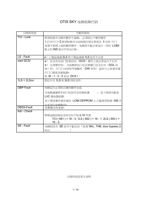
OTIS SKY 电梯故障代码
闪烁的信息英文说明
10.2.2.5 Blinking Event Messages
10.2.2.6 Event Logging
SSS
变频器故障代码表iai u&canea eve nr aescnpuon uoie
附加说明
10.1 J.8 Additional infonrational messages
These messages appear only in tiie slate display. 口即are not siored in the event logging.
TCBC板上垂直方向排列12个ELD显示电梯状态
发光二极管编发光二极管英文名详细解释正常时的状
号称态
ELD1BC阀门/制动器电流控制装置灭
ELD2VLC电压检测(5VDC亮
ELD3GRP/J群控/进线电源故障灭
ELD4NOR/DIAG正常操作检验灭
ELD5INS检修操作亮
ELD6ES急停灭
ELD7DW厅门信号亮
ELD8DFC门完全关闭亮
ELD9DOL开门限位灭
ELD10DOB开门按钮灭
ELD11DZ轿厢在门区信号亮
ELD12RSL远程串行通讯信号闪烁
TCBC/GEC左下方有四个开关作用
开关代号开关英文名称开关功能说明
SW1CHCS切断外呼
SW2DDO取消门操作
SW3CTTL呼梯到顶层
SW4CTBL呼梯到底层
范文素材和资料部分来自网络,供参考。
可复制、编制,期待你的好评与关注)。
G网告警预处理手册(华为G9MGW)

中国移动通信集团湖北有限公司网管中心预处理手册(华为MSC-MGW)【设备型号】:UMG8900【设备类型】:MGW【硬件平台】:OSTA【软件版本】:UMG8900V200R003/ UMG8900V200R005【预处理手册版本】:V1.1【本次版本更新时间】:2007年7月目录目录 (1)1、严重告警 (4)§1.1虚拟媒体网关迁移出业务态(ALM:1802) (4)§1.2主备倒换失败(ALM:0001) (6)§1.3 单板硬件故障(ALM:0007) (7)§1.4 单板硬件模块故障(ALM:0021) (9)§1.5 单板故障(ALM:0040) (10)§1.6 单机框不可用(ALM:0041) (11)§1.7 硬盘空间拥塞(ALM:1412) (12)§1.8 SPF扣板故障(ALM:3902) (13)§1.9 接口芯片异常(ALM:2633) (14)§1.10 逻辑工作不正常(ALM:2634) (15)§1.11 SDH信号丢失LOS(ALM:1201) (15)§1.12 SDH帧定位丢失(ALM:1202) (16)§1.13 接口故障(ALM:3209) (17)§1.14 M3UA目的实体路由无效(ALM:3991) (19)§1.15 M3UA路由无效(ALM:3992) (20)§1.16 M3UA目的信令点不可达(ALM:3993) (22)§1.17 MTP3目的信令点不可达(ALM:3980) (23)§1.18 L2UA链路组故障(ALM:3905) (25)2、重要告警 (27)§2.1 接收信号丢失(ALM:2601) (27)§2.2 接收时钟丢失(ALM:2602) (28)§2.3 CPU拥塞(ALM:1402) (30)§2.4 硬盘空间过载(ALM:1411) (31)§2.5 MBLU单板芯片故障(ALM:2001) (32)§2.6 FLU故障(ALM:2006) (33)§2.7 SPF扣板CPU过载(ALM:3850) (34)§2.8 配电框电路电源故障告警(ALM:317) (35)§2.9 TC U或VPU或ECU单板硬件告警(ALM:1613) (35)§2.10 BAM系统文件损坏告警(ALM:270) (36)§2.11 FE级联网口故障(ALM:0026) (37)§2.12 单板控制网口故障(ALM:37) (38)§2.13 GE级联光口故障(ALM:605) (39)§2.14 级联光口故障(ALM:807) (40)§2.15 级联链路连接与配置不符(ALM:818) (41)§2.16 级联链路连接错误(ALM:819) (42)§2.17 GE通道故障(ALM:1606) (43)§2.18 GE通道光模块故障(ALM:2002) (44)§2.19 GE通道CDR故障(ALM:2003) (45)§2.20 TDM通道光模块故障(ALM:2004) (45)§2.21 参考源丢失(ALM:2202) (46)§2.22 恒温晶体输出信号丢失(ALM:2204) (48)§2.23 时分交换芯片时钟丢失(ALM:2631) (50)§2.24 时分交换芯片时钟未锁定(ALM:2632) (51)§2.25 单板时钟故障(ALM:804) (52)§2.26 NET板主用时钟失锁(ALM:808) (53)§2.27 BLU时钟故障(ALM:2007) (54)§2.28 DDS输出信号丢失(ALM:2206) (55)§2.29 时钟丢失(ALM:2407) (57)§2.30 38M时钟故障(ALM:2524) (58)§2.31 34M/45M时钟故障(ALM:2527) (58)§2.32 12M时钟故障(ALM:2528) (59)§2.33 77M时钟丢失(ALM:2635) (59)§2.34 32M时钟丢失(ALM:2636) (60)§2.35 2K时钟丢失(ALM:2637) (61)§2.36 38M时钟丢失(ALM:3258) (61)§2.37 SPF时钟丢失(ALM:3900) (62)§2.38 SCTP信令链路拥塞(ALM:407) (64)§2.39 信令链路故障告警(ALM:409) (66)§2.40 信令半永久连接故障(ALM:802) (68)§2.41 M3UA链路故障(ALM:1250) (69)§2.42 M3UA链路故障(ALM:3990) (70)§2.43 SPF扣板链路故障(ALM:3851) (72)§2.44 L2UA链路拥塞(ALM:3904) (73)§2.45 MTP链路(ALM:3981) (74)§2.46 M3UA链路SCTP拥塞(ALM:3994) (75)3、次要告警 (77)§3.1 E1/T1时钟信号丢失(ALM:2401) (77)§3.2 E1/T1告警指示(ALM:2402) (78)§3.3 E1/T1远端告警(ALM:2403) (79)1、严重告警§1.1虚拟媒体网关迁移出业务态(ALM:1802)【告警标题(网管呈现)】:虚拟媒体网关迁移出业务态【告警标题含义】:当虚拟媒体网关因某种外界原因迁移出业务态时产生此告警。
Silicon Laboratories Flex SDK 3.3.0.0 产品说明书

Proprietary Flex SDK 3.3.0.0 GAGecko SDK Suite 4.0December 15, 2021less applications.Per its namesake, Flex offers two implementation options.The first uses Silicon Labs RAIL (Radio Abstraction Interface Layer), an intuitive and eas-ily-customizable radio interface layer designed to support both proprietary and standards-based wireless protocols.The second uses Silicon Labs Connect, an IEEE 802.15.4-based networking stack de-signed for customizable broad-based proprietary wireless networking solutions that re-quire low power consumption and operates in either the sub-GHz or 2.4 GHz frequencybands. The solution is targeted towards simple network topologies.The Flex SDK is supplied with extensive documentation and sample applications. All ex-amples are provided in source code within the Flex SDK sample applications.These release notes cover SDK version(s):3.3.0.0 GA released December 15, 2021Compatibility and Use NoticesFor information aboutsecurity updates and notices, see the Security chapter of the Gecko Platform Release notes installed with this SDK or on the Silicon Labs Release Notes page. Silicon Labs also strongly recommends that you subscribe to Security Advisories for up-to-date information. For instructions, or if you are new to the Silicon Labs Flex SDK, see Using This Release.Compatible Compilers:IAR Embedded Workbench for ARM (IAR-EWARM) version 8.50.9•Using wine to build with the IarBuild.exe command line utility or IAR Embedded Workbench GUI on macOS or Linux could result in incorrect files being used due to collisions in wine’s hashing algorithm for generating short file names.•Customers on macOS or Linux are advised not to build with IAR outside of Simplicity Studio. Customers who do should carefully verify that the correct files are being used.GCC (The GNU Compiler Collection) version 10.2.1, provided with Simplicity Studio.Contents Contents1Connect Applications (1)1.1New Items (1)1.2Improvements (1)1.3Fixed Issues (1)1.4Known Issues in the Current Release (1)1.5Deprecated Items (1)1.6Removed Items (1)2Connect Stack (2)2.1New Items (2)2.2Improvements (2)2.3Fixed Issues (2)2.4Known Issues in the Current Release (2)2.5Deprecated Items (2)2.6Removed Items (2)3RAIL Applications (3)3.1New Items (3)3.2Improvements (3)3.3Fixed Issues (3)3.4Known Issues in the Current Release (3)3.5Deprecated Items (3)3.6Removed Items (3)4RAIL Library (4)4.1New Items (4)4.2Improvements (4)4.3Fixed Issues (4)4.4Known Issues in the Current Release (5)4.5Deprecated Items (5)4.6Removed Items (5)5Using This Release (6)5.1Installation and Use (6)5.2Security Information (6)5.3Support (7)Connect Applications 1 Connect Applications1.1 New ItemsEFR32XG23 SupportBRD4002A Support1.2 ImprovementsNone1.3 Fixed IssuesNone1.4 Known Issues in the Current ReleaseIssues in bold were added since the previous release. If you have missed a release, recent release notes are available on https:///products/software.652925 EFR32XG21 is not supported for “Flex (Connect) - SoC LightExample DMP” and “Flex (Connect) - SoC Switch Example”1.5 Deprecated ItemsNone1.6 Removed ItemsNoneConnect Stack 2 Connect Stack2.1 New ItemsNone2.2 ImprovementsNone2.3 Fixed Issues754930 Fixed an issue that was causing emberStopTxStream to fail when the parent support plugin is not installed.2.4 Known Issues in the Current ReleaseIssues in bold were added since the previous release. If you have missed a release, recent release notes are available on https:///products/software.501561 In the Legacy HAL component,the PA configuration is hard-coded regardless of the user or board settings. Until this is changed to properly pull from the configuration header, the file ember-phy.c in the user's project will need to be modified by hand to reflect the desired PA mode, voltage, and ramp time.711804Connecting multiple devices simultaneously may fail with a timeout error.2.5 Deprecated ItemsNone2.6 Removed ItemsNoneRAIL Applications 3 RAIL Applications3.1 New Items•EFR32XG23 Support•BRD4002A Support•PSM Support for EFR32XG23, demonstrated by Flex (RAIL) - Long Preamble Duty Cycle•Wi-SUN FSK Support for:•Flex (RAIL) - Range Test•Flex (RAIL) - Simple TRX3.2 ImprovementsThe Range Test Applications can be used purely via CLI (LCD and Buttons can be uninstalled)3.3 Fixed IssuesNone3.4 Known Issues in the Current ReleaseNone3.5 Deprecated ItemsNone3.6 Removed ItemsNone4 RAIL Library4.1 New ItemsAdded in release 4.0.0.0•Added support for the ZGM230SA27HGN, ZGM230SA27HNN, and ZGM230SB27HGN modules.•Added RAIL_GetTxPacketsRemaining() API for use when handling one of the RAIL_EVENTS_TX_COMPLETION to get a sense of how many transmits remain in a RAIL_SetNextTxRepeat() sequence.•Added PA curves for HP, MP, LP and LLP modes on all EFR32xG23 radio boards.•Added RAIL_PA_BAND_COUNT to count RAIL_PaBand_t.•Added a new RAIL_RxDataSource_t to capture direct mode data on supported devices.•Added a new RAIL_IEEE802154_Config2p4GHzRadioCustom1 API to configure an alternate IEEE 802.15.4 PHY with slightly dif-ferent performance characteristics for the EFR32xG12 and EFR32xG13 parts. Use this API if instructed by Silicon Labs for your use case.4.2 ImprovementsChanged in release 4.0.0.0•Added IEEE802.15.4 Coexistence and FEM PHYs to EFR32xG12 and EFR32xG13 based modules.•Updated IEEE802.15.4 FEM PHYs on EFR32xG12 and EFR32xG13 based modules for improved performance.•Updated all header files to have extern "C" when being built with C++ for compatibility.•Made the RAIL_EnableRxDutyCycle() API safe to call in a multiprotocol application.•To save both flash and RAM, moved information formerly contained in RAIL_Config_t::protocol, RAIL_Config_t::scheduler, and RAIL_Config_t::buffer internal to RAIL and sized appropriately for single vs. multiprotocol. RAIL multiprotocol now provides two internal state buffers for two protocols by default. An application that needs more must now call RAIL_AddStateBuffer3() or RAIL_AddStateBuffer4() to add a 3rd and 4th buffer, respectively. Otherwise RAIL_Init() will fail when trying to initialize a 3rd or 4th protocol.•"RAIL Utility, Coexistence" component GPIO interrupt numbers are now chosen at runtime to avoid conflicts.• A new RAIL API RAIL_GetSchedulerStatusAlt will now return more descriptive radio scheduler events as well as the RAIL_Status_t of the RAIL API invoked by the radio scheduler. As a part of the new API, new RAIL_SchedulerStatus_t events have been added while retaining the previous ones for backwards compatibility. Note that the underlying values of the existing RAIL_SchedulerStatus_t events may have changed.•Updated the RAIL_IEEE802154_Config2p4GHzRadio*Fem PHYs on the EFR32xG12 and EFR32xG13 devices to improve perfor-mance.•The example CSV files referred to in AN1127: Power Amplifier Power Conversion Functions in RAIL 2.x are updated with realistic values.4.3 Fixed IssuesFixed in release 4.0.0.0646980 An attempt to use an unsupported built-in radio channel configuration, e.g., on a module that does not support that protocol or configuration, will now trip RAIL_ASSERT_FAILED_INVALID_CHANNEL_CONFIG rather than returningsuccess and ignoring the configuration.671651 Fixed timing problems with certain State_Transitions or Rx_Channel_Hopping delay values on the EFR32xG22 and newer parts.682739 Fixed an issue with the BLE coded PHY's modulation index on the EFR32xG21 parts that could cause deviation measurements to fail.714271 Fixed an issue where RAIL_IEEE802154_Config2p4GHzRadio*() and RAIL_IEEE802154_ConfigGB*Radio() functions were improperly clearing or setting certain RAIL_IEEE802154_EOptions_t. Also documented that thesefunctions still implicitly clear or set certain RAIL_IEEE802154_GOptions_t suitable for that configuration.716369 Fixed an issue where incorrect radio transition times were being applied at higher temperatures when using the high power PA on EFR32xG22 parts.723098 Fixed RAIL_SetFixedLength(handle, RAIL_SETFIXEDLENGTH_INVALID) to restore dynamic frame length operation if the current PHY was originally configured for that.738931 Fixed an issue with the BLE Coded PHYs on the EFR32xG22 device that could cause some packets to be improperly sent and not trigger a RAIL_EVENT_TX_PACKET_SENT event.739594 Fix an issue with the RX_IQDATA_FILTLSB RAIL_RxDataSource_t on EFR32xG23 parts where the data did not properly saturate and was instead just the lower 16 bits of IQ sample data.744323 Fixed an issue when using BLE AoX where non-AoX packets were transmitted on an undefined antenna. They will now always use the first antenna in the configured RAIL_BLE_AoxConfig_t::antArrayAddr pattern.745528 Fixed some incorrect RAIL_RxPacketInfo_t::filterMask values for 802.15.4 ACKs when promiscuous, or when the PanId coordinator received a packet with only source PanId and no destination address.753860 Fixed an issue when running IR Calibration on the EFR32xG23 (RAIL_CalibrateIrAlt) where we could compute a completely invalid IRCAL value for certain PHYs and chips.754219 Increase maximum BLE coex request window setting, SL_RAIL_UTIL_COEX_REQ_WINDOW, in "RAIL Utility, Coexistence" component from 255 to 5000.4.4 Known Issues in the Current ReleaseIssues in bold were added since the previous release. If you have missed a release, recent release notes are available on https:///products/software.Using direct mode (or IQ) functionality on EFR32xG23requires a specifically set radio configuration that is notyet supported by the radio configurator. For theserequirements, reach out to technical support who couldprovide that configuration based on your specification641705 Infinite receive operations where the frame's fixed lengthis set to 0 are not working correctly on the EFR32xG23series chips.732659 On EFR32xG23:•Wi-SUN FSK mode 1a exhibits a PER floor with fre-quency offsets around ± 8 to 10 KHz• Wi-SUN FSK mode 1b exhibits a PER floor with fre-quency offsets around ± 18 to 20 KHz4.5 Deprecated ItemsNone4.6 Removed ItemsNone5 Using This ReleaseThis release contains the following•Radio Abstraction Interface Layer (RAIL) stack library•Connect Stack Library•RAIL and Connect Sample Applications•RAIL and Connect Components and Application FrameworkThis SDK depends on Gecko Platform. The Gecko Platform code provides functionality that supports protocol plugins and APIs in the form of drivers and other lower layer features that interact directly with Silicon Labs chips and modules. Gecko Platform components include EMLIB, EMDRV, RAIL Library, NVM3, and mbedTLS. Gecko Platform release notes are available through Simplicity Studio’s Documentation tab.For more information about the Flex SDK v3.x see UG103.13: RAIL Fundamentals and UG103.12: Silicon Labs Connect Fundamentals. If you are a first time user, see QSG168: Proprietary Flex SDK v3.x Quick Start Guide.5.1 Installation and UseThe Proprietary Flex SDK is provided as part of the Gecko SDK (GSDK), the suite of Silicon Labs SDKs. To quickly get started with the GSDK, install Simplicity Studio 5, which will set up your development environment and walk you through GSDK installation. Simplicity Studio 5 includes everything needed for IoT product development with Silicon Labs devices, including a resource and project launcher, software configuration tools, full IDE with GNU toolchain, and analysis tools. Installation instructions are provided in the online Simplicity Studio 5 User’s Guide.Alternatively, Gecko SDK may be installed manually by downloading or cloning the latest from GitHub. See https:///Sili-conLabs/gecko_sdk for more information.Simplicity Studio installs the GSDK by default in:•(Windows): C:\Users\<NAME>\SimplicityStudio\SDKs\gecko_sdk•(MacOS): /Users/<NAME>/SimplicityStudio/SDKs/gecko_sdkDocumentation specific to the SDK version is installed with the SDK. Additional information can often be found in the knowledge base articles (KBAs). API references and other information about this and earlier releases is available on https:///.5.2 Security InformationSecure Vault IntegrationThis version of the stack does not integrate Secure Vault Key Management.Security AdvisoriesTo subscribe to Security Advisories, log in to the Silicon Labs customer portal, then select Account Home. Click HOME to go to the portal home page and then click the Manage Notifications tile. Make sure that ‘Software/Security Advisory Notices & Product Change Notices (PCNs)’ is checked, and that you are subscribed at minimum for your platform and protocol. Click Save to save any changes.5.3 SupportDevelopment Kit customers are eligible for training and technical support. Use the Silicon Labs Flex web page to obtain information about all Silicon Labs Thread products and services, and to sign up for product support.You can contact Silicon Laboratories support at /support.Silicon Laboratories Inc.400 West Cesar Chavez Austin, TX 78701USAIoT Portfolio/IoTSW/HW/simplicityQuality /qualitySupport & Community/communityDisclaimerSilicon Labs intends to provide customers with the latest, accurate, and in-depth documentation of all peripherals and modules available for system and software imple-menters using or intending to use the Silicon Labs products. Characterization data, available modules and peripherals, memory sizes and memory addresses refer to each specific device, and “Typical” parameters provided can and do vary in different applications. Application examples described herein are for illustrative purposes only. Silicon Labs reserves the right to make changes without further notice to the product information, specifications, and descriptions herein, and does not give warranties as to the accuracy or completeness of the included information. Without prior notification, Silicon Labs may update product firmware during the manufacturing process for security or reliability reasons. Such changes will not alter the specifications or the performance of the product. Silicon Labs shall have no liability for the consequences of use of the infor -mation supplied in this document. This document does not imply or expressly grant any license to design or fabricate any integrated circuits. The products are not designed or authorized to be used within any FDA Class III devices, applications for which FDA premarket approval is required or Life Support Systems without the specific written consent of Silicon Labs. A “Life Support System” is any product or system intended to support or sustain life and/or health, which, if it fails, can be reasonably expected to result in significant personal injury or death. Silicon Labs products are not designed or authorized for military applications. Silicon Labs products shall under no circumstances be used in weapons of mass destruction including (but not limited to) nuclear, biological or chemical weapons, or missiles capable of delivering such weapons. Silicon Labs disclaims all express and implied warranties and shall not be responsible or liable for any injuries or damages related to use of a Silicon Labs product in such unauthorized applications. Note: This content may contain offensive terminology that is now obsolete. Silicon Labs is replacing these terms with inclusive language wherever possible. For more information, visit /about-us/inclusive-lexicon-projectTrademark InformationSilicon Laboratories Inc.®, Silicon Laboratories ®, Silicon Labs ®, SiLabs ® and the Silicon Labs logo ®, Bluegiga ®, Bluegiga Logo ®, EFM ®, EFM32®, EFR, Ember ®, Energy Micro, Energy Micro logo and combinations thereof, “the world’s most energy friendly microcontrollers”, Redpine Signals ®, WiSeConnect , n-Link, ThreadArch ®, EZLink ®, EZRadio ®, EZRadioPRO ®, Gecko ®, Gecko OS, Gecko OS Studio, Precision32®, Simplicity Studio ®, Telegesis, the Telegesis Logo ®, USBXpress ® , Zentri, the Zentri logo and Zentri DMS, Z-Wave ®, and others are trademarks or registered trademarks of Silicon Labs. ARM, CORTEX, Cortex-M3 and THUMB are trademarks or registered trademarks of ARM Holdings. Keil is a registered trademark of ARM Limited. Wi-Fi is a registered trademark of the Wi-Fi Alliance. All other products or brand names mentioned herein are trademarks of their respective holders.。
LTE系统S1AP协议研究

LTE系统S1AP协议研究何炜文;卢宪祺【摘要】LTE system is the evolution version of 3GPP the third generation mobile communication system.S1AP protocol,an application layer protocol of interface S1-MME between the access network and the core network,controls the signaling and data transmission between the access network and the core network.The functions and elementary procedures of S1AP protocol are described and summarized,and the E-RAB setup procedure,initial context setup procedure,paging procedure and NAS transport procedure are focused on,which is helpful to further research of S1AP protocol.%LTE系统是3GPP推出的第三代移动通信系统的演进版本。
S1AP协议作为其接入网和核心网接口S1-MME的一个应用层协议,控制着接入网和核心网之间信令和数据的传输。
为研究S1AP协议,就S1AP协议的功能和相关的基本过程进行了描述和总结,并重点阐述了E-RAB建立过程、初始上下文建立过程、寻呼过程和NAS传输过程等典型的S1AP基本过程。
这对进一步研究S1AP 协议有一定的帮助。
【期刊名称】《北京联合大学学报(自然科学版)》【年(卷),期】2011(025)004【总页数】4页(P15-18)【关键词】LTE;S1-MME;S1AP;基本过程【作者】何炜文;卢宪祺【作者单位】北京邮电大学计算机学院,北京100876;北京邮电大学计算机学院,北京100876【正文语种】中文【中图分类】TN929.5330 引言LTE(Long Term Evolution)系统是3GPP推出的第三代移动通信系统(3G)的演进版本,它被称为3.9G,被视为从3G向4G演进的主流技术。
DM9000中文手册

,011)被选 中
访问类型 高电平
是访问数据 端口;低电平 是访问地址 端口
字命令标志, 默认低电平 有效
当访问 外部数据存 储器是字或 双字宽度时, 被置位
100
INT
O
中断请求信 号
高电平 有效,极性能 修改
37~53 56
SD31~16
I/O
双字模式,高 16 位数据引 脚
注意:以上介质无关端口都内部自带 60K 欧姆的下拉电阻 处理器接口引脚
1
IOR#
I
2
IOW#
I
3
AEN#
I
处理器读命 令
低电平 有效,极性能 够被 EEPRO M 修改,详细 请参考对 EE PROM 内容 的描述
处理器写命 令
低电平 有效,同样能 修改极性
芯片选择,低
4
IOWAIT
O
14
RST
外部介质无 关接口发送 时钟
外部介质无 关接口发送 数据低 4 位
输出
TXD[2: 0]决定内部 存储空间基 址:TXD [2: 0]) * 10H +
300H
54
MDIO
I/O
外部介质无
关接口串行
数据通信
57
MDC
O
外部介质无 关串行数据 通信口时钟, 且与中断引 脚有关
该引脚 高电平时候, 中断引脚低 电平有效;否 则高有效
0 0 16 位
0 1 32 位
108 位
11未 定义
66
EECK
I
时钟信号
67
EECS
I/O
片选
也做 LE D 模式选择 引脚
- 1、下载文档前请自行甄别文档内容的完整性,平台不提供额外的编辑、内容补充、找答案等附加服务。
- 2、"仅部分预览"的文档,不可在线预览部分如存在完整性等问题,可反馈申请退款(可完整预览的文档不适用该条件!)。
- 3、如文档侵犯您的权益,请联系客服反馈,我们会尽快为您处理(人工客服工作时间:9:00-18:30)。
4.3 Remote Port User InterfaceThe Remote Port of the DM240 allows for complete control and monitor functions via an RS-485 Serial Interface.Control and status messages are conveyed between the DM240 and the subsidiary modems, and the host computer using packetized message blocks in accordance with a proprietary communications specification. This communication is handled by the Radyne Link Level Protocol (RLLP), which serves as a protocol ‘wrapper’ for the M&C data.Complete information on monitor and control software is contained in the following sections.4.3.1 Protocol StructureThe Communications Specification (COMMSPEC) defines the interaction of computer resident Monitor and Control software used in satellite earth station equipment such as modems, redundancy switches, multiplexers, and other ancillary support gear. Communication is bi-directional, and is normally established on one or more full-duplex multi-drop control buses that conform to EIA Standard RS-485.Each piece of earth station equipment on a control bus has a unique physical address, which is assigned during station setup/configuration or prior to shipment. Valid decimal addresses on one control bus range from 032 through 255 for a total of up to 224 devices per bus. Address 255 of each control bus is usually reserved for the M&C computer.4.3.2 Protocol WrapperThe Radyne COMMSPEC is byte-oriented, with the Least Significant Bit (LSB) issued first. Each data byte is conveyed as mark/space information with two marks comprising the stop data. When the last byte of data is transmitted, a hold comprises one steady mark (the last stop bit). To begin or resume data transfer, a space substitutes this mark. This handling scheme is controlled by the hardware and is transparent to the user. A pictorial representation of the data and its surrounding overhead may be shown as follows:S1S2B0B1B2B3B4B5B6B7S1S2, etc. The stop bits, S1 and S2, are each a mark. Data flow remains in a hold mode until S2 is replaced by a space. If S2 is followed by a space, it is considered a start bit for the data byte and not part of the actual data (B0 - B 7).The COMMSPEC developed for use with the Radyne Link Level Protocol (RLLP) organizes the actual monitor and control data within a shell, or "protocol wrapper", that surrounds the data. The format and structure of the COMMSPEC message exchanges are described herein. Decimal numbers have no suffix; hexadecimal numbers end with a lower case h suffix and binary values have a lower case b suffix. Thus, 22 = 16h = 000010110b. The principal elements of a data frame, in order of occurrence, are summarized as follows:<SYNC> - the message format header character, or ASCII sync character, that defines the beginning of a message. The <SYNC> character value is always 16h.<BYTE COUNT> - the Byte Count is the number of bytes in the <DATA> field, ranging from 0 through TBD. This field is 2 bytes long for the DM240 protocol.<SOURCE ID> - the Source Identifier defines the message originator’s multidrop address. Note that all nodes on a given control bus have a unique address that must be defined.<DESTINATION ID> - The Destination Identifier specifies the multidrop address of the device(s) to which the message is sent.<FRAME SEQUENCE NUMBER> - The FSN is a tag with a value from 0 through 255 that is sent with each message. It assures sequential information framing and correct equipment acknowledgment and data transfers.<OPCODE> - The Operation Code field contains a number that identifies the message type associated with the data that follows it. Acknowledgment and error codes are returned in this field. This field is 2 Bytes for the DM240 protocol.<...DATA...> - The Data field contains the binary, data bytes associated with the <OPCODE>.The number of data bytes in this field is indicated by the <BYTE COUNT> value.<CHECKSUM> - The checksum is the modulo 256 sum of all preceding message bytes, excluding the <SYNC> character. The checksum determines the presence or absence of errors within the message. In a message block with the following parameters, the checksum is computed as shown below in Table 4-4.Table 4-4. Checksum Calculation ExampleBYTE FIELD DATA CONTENT RUNNING CHECKSUM <BYTE COUNT> (Byte 1) 00h = 00000000b 00000000b<BYTE COUNT> (Byte 2) 02h = 00000010b 00000010b <SOURCEID> F0h = 11110000b 11110010b <DESTINATION ID> 2Ah = 00101010b 00011100b <FSN> 09h = 00001001b 00100101b <OPCODE> (Byte 1) 00h = 00000000b 00101000b<OPCODE> (Byte 2) 03h = 00000011b 00101000b<DATA> (Byte 1) DFh = 11011111b 00000111b<DATA> (Byte 2) FEh = 11111110b 00000101bThus, the checksum is 00000101b; which is 05h or 5 decimal. Alternative methods of calculating the checksum for the same message frame are:00h + 02h + F0h + 2Ah + 09h + 00h + 03h + DFh + FEh = 305h.Since the only concern is the modulo 256 (modulo 100h) equivalent (values that can be represented by a single 8-bit byte), the checksum is 05h.For a decimal checksum calculation, the equivalent values for each information field are:0 + 2 + 240 + 42 + 9 + 0 + 3 + 223 + 254 = 773;773/256 = 3 with a remainder of 5. This remainder is the checksum for the frame.5 (decimal) = 05h = 0101b = <CHECKSUM>4.3.3 Frame Description and Bus HandshakingIn a Monitor and Control environment, every message frame on a control bus port executes as a packet in a loop beginning with a wait-for-SYN-character mode. The remaining message format header information is then loaded, either by the M&C computer or by a subordinate piece of equipment requesting access to the bus. Data is processed in accordance with the OPCODE, and the checksum for the frame is calculated. If the anticipated checksum does not match then the wait-for-SYN mode goes back into effect. If the OPCODE resides within a command message, it defines the class of action that denotes an instruction that is specific to the device type, and is a prefix to the DATA field if data is required. If the OPCODE resides within a query message packet, then it defines the query code, and can serve as a prefix to query code DATA. The Frame Sequence Number (FSN) is included in every message packet, and increments sequentially. When the M & C computer or bus-linked equipment initiates a message, it assigns the FSN as a tag for error control and handshaking. A different FSN is produced for each new message from the FSN originator to a specific device on the control bus. If a command packet is sent and not received at its intended destination, then an appropriate response message is not received by the packet originator. The original command packet is then re-transmitted with the same FSN. If the repeated message is received correctly at this point, it is considered a new message and is executed and acknowledged as such.If the command packet is received at its intended destination but the response message (acknowledgment) is lost, then the message originator (usually the M&C computer) re-transmits the original command packet with the same FSN. The destination device detects the same FSN and recognizes that the message is a duplicate, so the associated commands within the packet are not executed a second time. However, the response packet is again sent back to the source as an acknowledgment in order to preclude undesired multiple executions of the same command. To reiterate, valid equipment responses to a message require the FSN tag in the command packet. This serves as part of the handshake/acknowledge routine. If a valid response message is absent, then the command is re-transmitted with the same FSN. For a repeat of the same command involving iterative processes (such as increasing or decreasing transmit power level), the FSN is incremented after each message packet. When the FSN value reaches 255, it overflows and begins again at zero.The full handshake/acknowledgment involves a reversal of source and destination ID codes in the next message frame, followed by a response code in the <OPCODE> field of the message packet from the equipment under control.4.3.4 Global Response Operational CodesIn acknowledgment (response) packets, the operational code <OPCODE> field of the message packet is set to 0 by the receiving devices when the message intended for the device is evaluated as valid. The device that receives the valid message then exchanges the <SOURCE ID> with the <DESTINATION ID> sets the <OPCODE> to zero in order to indicate that a good message was received, and returns the packet to the originator. This "GOOD MESSAGE" Opcode is one of nine global responses. Global response Opcodes are common responses, issued to the M&C computer or to another device, that can originate from and are interpreted by all Radyne equipment in the same manner. These are summarized as follows (all Opcode values are expressed in decimal form):RESPONSE OPCODE DESCRIPTION OPCODEGood Message 00hBad Parameter FFhBad Opcode FEh4.3.5 Collision AvoidanceWhen properly implemented, the physical and logical devices and ID addressing scheme of the COMMSPEC normally precludes message packet contention on the control bus. The importance of designating unique IDs for each device during station configuration cannot be overemphasized. One pitfall, which is often overlooked, concerns multi-drop override IDs. All too often, multiple devices of the same type are assigned in a direct-linked ("single-thread") configuration accessible to the M&C computer directly. For example, if two DM240 Modulators with different addresses (DESTINATION IDs) are linked to the same control bus at the same hierarchical level, both will attempt to respond to the M&C computer when the computer generates a multi-drop override ID of 23. If their actual setup parameters, status, or internal timing differs, they will both attempt to respond to the override simultaneously with different information, or asynchronously in their respective message packets and response packets, causing a collision on the serial control bus.To preclude control bus data contention, different IDs must always be assigned to the equipment. If two or more devices are configured for direct-linked operation, then the M&C computer and all other devices configured in the same manner must be programmed to inhibit broadcast of the corresponding multi-drop override ID.The multi-drop override ID is always accepted by devices of the same type on a common control bus, independent of the actual DESTINATION ID. These override IDs with the exception of “BROADCAST” are responded to by all directly linked devices of the same type causing contention on the bus. The “BROADCAST” ID, on the other hand, is accepted by all equipment but none of them returns a response packet to the remote M&C.The following multi-drop override IDs are device-type specific, with the exception of "BROADCAST". These are summarized below with ID values expressed in decimal notation: Directly-Addressed Equipment Multi-Drop Override ID Broadcast (all directly-linked devices) 00DMD-3000/4000, 4500 or 5000 Mod Section, DMD15 01DMD-3000/4000, 4500 or 5000 Demod Section, DMD15 02RCU-340 1:1 Switch 03RCS-780 1:N Switch 04RMUX-340 Cross-Connect Multiplexer 05CDS-780 Clock Distribution System 06SOM-340 Second Order Multiplexer 07DMD-4500/5000 Modulator Section 08DMD-4500/5000 Demodulator Section 09RCU-5000 M: N Switch 10DMD15 Modulator 20DMD15 Demodulator 21DMD15 Modem 22DVB3030 Video Modulator, DM240 23Reserved for future equipment types 24-31Note that multi-drop override ID 01 can be used interchangeably to broadcast a message to a DMD-3000/4000 modem, a DMD-4500/5000, a DMD15 modem, or a DVB3030. Radyne Corp. recommends that the multi-drop override IDs be issued only during system configuration as a bus test tool by experienced programmers, and that they not be included in run-time software. It is also advantageous to consider the use of multiple bus systems where warranted by a moderate to large equipment complement.Therefore, if a DMD15 Modulator is queried for its equipment type identifier, it will return a "20" and DMD15 Demodulator will return a "21". A DMD15 Modem will also return an "22". A DVB3030 Video Modulator will return a “23.”4.3.6 Software CompatibilityThe COMMSPEC, operating in conjunction within the RLLP shell, provides for full forward and backward software compatibility independent of the software version in use. New features are appended to the end of the DATA field without OPCODE changes. Older software simply discards the data as extraneous information without functional impairment for backward compatibility.If new device-resident or M&C software receives a message related to an old software version, new information and processes are not damaged or affected by the omission of data.The implementation of forward and backward software compatibility often, but not always, requires the addition of new Opcodes. Each new function requires a new Opcode assignment if forward and backward compatibility cannot be attained by other means.When Radyne equipment is queried for bulk information (Query Mod, Query Demod, etc.) it responds by sending back two blocks of data; a Non-Volatile Section (parameters that can be modified by the user) and a Volatile Section (status information). It also returns a count value that indicates how large the Non-Volatile Section is. This count is used by M&C developers to index into the start of the Volatile Section.When new features are added to Radyne equipment, the control parameters are appended to the end of the Non-Volatile Section, and status of the features, if any, are added at the end of the Volatile Section. If a remote M&C queries two pieces of Radyne equipment with different revision software, they may respond with two different sized packets. The remote M&C MUST make use of the non-volatile count value to index to the start of the Volatile Section. If the remote M&C is not aware of the newly added features to the Radyne product, it should disregard the parameters at the end of the Non-Volatile Section and index to the start of the Volatile Section.If packets are handled in this fashion, there will also be backward-compatibility between Radyne equipment and M&C systems. Remote M&C systems need not be modified every time a feature is added unless the user needs access to that feature.4.3.7 RLLP SummaryThe RLLP is a simple send-and-wait protocol that automatically re-transmits a packet when an error is detected, or when an acknowledgment (response) packet is absent.During transmission, the protocol wrapper surrounds the actual data to form information packets. Each transmitted packet is subject to time out and frame sequence control parameters, after which the packet sender waits for the receiver to convey its response. Once a receiver verifies that a packet sent to it is in the correct sequence relative to the previously received packet, it computes a local checksum on all information within the packet excluding the <SYN> character and the <CHECKSUM> fields. If this checksum matches the packet <CHECKSUM>, the receiver processes the packet and responds to the packet sender with a valid response (acknowledgment) packet.The response packet is therefore either an acknowledgment that the message was received correctly. If the sender receives a valid acknowledgment (response) packet from the receiver, the <FSN> increments and the next packet is transmitted as required by the sender.If an acknowledgment (response) packet is lost, corrupted, or not issued due to an error and is thereby not returned to the sender, the sender re-transmits the original information packet; but with the same <FSN>. When the intended receiver detects a duplicate packet, the packet is acknowledged with a response packet and internally discarded to preclude undesired repetitive executions. If the M&C computer sends a command packet and the corresponding response packet is lost due to a system or internal error, the computer times out and re-transmits the same command packet with the same <FSN> to the same receiver and waits once again for an acknowledgment.4.3.8 DM240 Opcode Command SetThe DM240 Opcode Command Set is listed below.4.3.9 Modulator Command SetCommand OpcodeQuery Mod All 2400hQuery Mod Latched Alarms 2405hQuery Mod Current Alarms 2408hQuery Mod Status 240BhQuery Time 240EhQuery Date 240FhQuery Time and Date 2410hQuery Firmware Part/Rev 2414hQuery AASI NULL PID (w/IPSat interface card only) 2456hQuery IPSat Burst Demod Count (w/IPSat interface card only) 2457hQuery IPSat Control PID (w/IPSat interface card only) 2458hQuery IPSat Enable (w/IPSat interface card only) 2459hQuery IPSat User Data Rate (w/IPSat interface card only) 245AhQuery PCR Restamping 245BhQuery Multi-PIIC Configuration (w/Multi-PIIC interface card only) 245ChQuery Multi-PIIC Status (w/Multi-PIIC interface card only) 245DhQuery RF Switch Status (w/RF Switch hardware only) 2560h Command Mod Configuration 2601h Command Mod Single Parameter:FrequencyData Rate Modulation Type 2602h 2604h 2606hInner FEC RateTx On/OffCarrier TestInput Clock ControlInput Clock PolarityTransmit Power LevelSpectrumReference SourceNetwork SpecificationExternal Reference FrequencyData PolarityTerrestrial Interface TypeTerrestrial Frame SizeCarrier Set Roll OffOutput Clock ControlSymbol RateAASI NULL PID (w/IPSat interface card only)IPSat Burst Demod Count (w/IPSat interface card only) IPSat Control PID (w/IPSat interface card only)IPSat Enable (w/IPSat interface card only) 2607h 2609h 260Ah 260Bh 260Ch 260Fh 2611h 2616h 2619h 261Bh 2620h 2621h 2640h 2641h 2642h 2643h 2656h 2657h 2658h 2659hCommand PCR Restamping 265Bh Command Multi-PIIC Configuration (w/Multi-PIIC interface cardonly)265Ch Command Clear Latched Alarms 2C03h Command Set Time 2C04h Command Set Date 2C05h Command Set Time and Date 2C06h Command RF Switch Redundancy Mode (w/RF Switchhardware only)2F40h Command RF Switch Fault Test (w/RF Switch hardware only) 2F41h Command RF Switch Active Side (w/RF Switch hardware only) 2F42h 4.3.10 Detailed Command DescriptionsOpcode: <2400h>(Query Mod All) Query a Modulator's Configuration and StatusQuery Response<1> NumberofNonvol bytesNumber of Configuration BytesConfiguration Bytes<4><2> <4> <4> <1><1> <1><1> <1> <1><1><2> <1> <1> <1> <1> <1><1> <1> <1> IF FrequencyReservedData RateExternalReferenceFrequencyReferenceSourceModulation TypeInner FEC RateReservedReservedReservedReservedTransmit PowerLevelCarrier ControlCarrier TestSpectrumReservedTx InterfaceTypeInput ClockPolarityData PolarityInput ClockSourceBinary Value, units Hz in 100 Hz steps.50000000 Hz to 180000000 Hz 70/140950000000 Hz to 2050000000 Hz L-BandTBDBinary Value, 1 bps stepsBinary Value, units Hz in 8000 Hz steps, e.g. 1000000 Hz,1008000 Hz, etc., range = 256000 Hz to 10000000 Hz0 = Internal, 1 = External0 = QPSK, 1 = BPSK, 2 = 8PSK, 3 = 16QAM1 = 1/2 Rate, 2 = 2/3 Rate, 3 = 3/4 Rate, 4 = 5/6 Rate,5 = 7/8Rate, 6 = 6/7 Rate, 7 = 4/5 Rate, 8 = 8/9 Rate, 9 = 9/10 Rate,128 = 1/4 Rate, 129 = 1/3 Rate, 130 = 2/5 Rate, 131 = 3/5RateTBD, Default = 1TBD, Default = 1TBD, Default = 0TBD, Default = 0Signed Value. +0 to –250 (+0.0 to –25.0 dBm) (two’scompliment)0 = Off, 1 = On0 = Off, 1 = CW, 2 = Dual, 3 = Offset, 4 = Pos FIR, 5 = NegFIR0 = Inverted, 1 = NormalTBD, 0 = Default0 = Serial, 1 = Parallel, 2 = ASI_Norm, 3 = ASI_Null, 4 =G.703E3, 5 = G.703 T3, 6 = G.703 STS-1, 7 = HSSI, 8 =Parallel DVB, 9 = Parallel M2P, 10 = None, 11 = DirecTV, 13= OC3, 14 = STM-1, 15 = G.703 E2, 16 = G.703 T2 Bal, 17 =G.703 T2 UNBAL, 18 = G.703 E1 Bal, 19 = G.703 E1 UNBAL,20 = G.703 T1 AMI 21 = G.703 T1 B8ZS0 = Normal, 1 = Inverted0 = Normal, 1 = Inverted0 = SCTE, 1 = SCT<1> <11> <1> <1><1><1><1> <4> <1> <1> <1> <1> <1><1> <1> <1> ReservedReservedReservedMajor AlarmMaskMinor AlarmMaskCommon FaultMaskReservedSymbol RateTerrestrialFramingRoll OffReservedOutput ClockSourceNetwork SpecScramblerBypassOuter FECBypassTest PatternTBD, Default = 0TBDTBDBit 0 = SpareBit 1 = Transmit Oversample PLL LockBit 2 = FPGA Config ErrorBit 3 = IF Synthesizer PLL LockBit 4 = External Reference PLL LockBit 5 = Composite (SCT) PLL LockBit 6 = Symbol PLL LockBit 7 = Spare0 = Mask, 1 = AllowBit 0 = Terrestrial Ethernet data activity detectBit 1 = Loss Terrestrial ClockBit 2 = Loss Terrestrial DataBit 3 = FIFO ErrorBit 4 = Output LevelBit 5 = Terrestrial Framing ErrorBit 6 = Terr Ethernet jitter buffer underflowBit 7 = Terr Ethernet jitter buffer overflow0 = Mask, 1 = AllowBit 0 = -12 V AlarmBit 1 = +12 V AlarmBit 2 = +5 V AlarmBits 3 – 7 = Spares0 = Mask, 1 = AllowTBD, Default = 0Symbol Rate in Symbols Per Second0 = 188 Byte, 1 = 204 Byte, 2 = No Framing, 3 = DirecPC, 4 =DirecTV0 = 0.35, 25 = 0.25, 1 = 0.20TBD0 = SCTE, 1 = SCT, 2 = None0 = DVB-S, 1 = Direct PC, 9 = DirecTV, 11 DVB-S2 BS NBC,12 = DVB-S2 BS BC, 13 = DirecTV AMC NBC, 14 = DirecTVAMC BC0 = Normal, 1 = Bypass0 = Normal, 1 = Bypass0 = None, 1 = 215 – 1, 23 = 223-1<1> <1> <1> <1><1> <1> <1><1> <1> <1> <1><1><2> <4> Last RateControlInterleaverBypassPCRRestampingMulti-PIIC ModeRedundancyModePrime PIIC SlotBackup PIICSlotPilot SymbolsInner FECBypassPL ScramblerBypassPL NoiseGeneratorEnablePL NoiseGeneratorProfilePL HeaderScrambler SeqIndexGold Code SeqIndex0 = Symbol Rate, 1 = Data Rate, 2 = Auto0 = Bypass, 1 = Normal0 = Off, 1= OnWithout Multi-PIIC Card:1 = ManualWith Multi-PIIC Card:1 = Manual,2 = RedundancyWithout Multi-PIIC Card or Manual Multi-PIIC Mode:With Multi-PIIC Card:0 = Force Prime,1 = Force Backup,2 = Manual Revert,3 = Auto-RevertWithout Multi-PIIC Card:1With Multi-PIIC Card:1 – 3Without Multi-PIIC Card:1With Multi-PIIC Card:1 – 30 = Off, 1 = On0 = Normal, 1 = Bypass0 = Normal, 1 = Bypass0 = Disable, 1 = Enable1 to 161 to 20000 to 262142Status Bytes<1> <1> <1> <1><1><1> <1> <1> <1> ReservedReservedReservedMajor AlarmMinor AlarmCommon FaultLatched MajorAlarmLatched MinorAlarmLatchedCommon FaultTBDTBDTBDBit 0 = SpareBit 1 = Transmit Oversample PLL LockBit 2 = FPGA Config ErrorBit 3 = IF Synthesizer PLL LockBit 4 = External Reference PLL LockBit 5 = Composite (SCT) PLL LockBit 6 = Symbol PLL LockBit 7 = Spare0 = Pass, 1 = FailBit 0 = Terrestrial Ethernet data activity detectBit 1 = Loss Terrestrial ClockBit 2 = Loss Terrestrial DataBit 3 = FIFO ErrorBit 4 = Output LevelBit 5 = Terrestrial Framing ErrorBit 6 = Terr Ethernet jitter buffer underflowBit 7 = Terr Ethernet jitter buffer overflow0 = Pass, 1 = FailBit 0 = -12 V Alarm. 1 = FailBit 1 = +12 V Alarm. 1 = FailBit 2 = +5 V Alarm. 1 = FailBits 3 - 7 = Spares0 = Pass, 1 = FailBit 0 = SpareBit 1 = Transmit Oversample PLL LockBit 2 = FPGA Config ErrorBit 3 = IF Synthesizer PLL LockBit 4 = External Reference PLL LockBit 5 = Composite (SCT) PLL LockBit 6 = Symbol PLL LockBit 7 = Spare0 = Pass, 1 = FailBit 0 = Terrestrial Ethernet data activity detectBit 1 = Loss Terrestrial ClockBit 2 = Loss Terrestrial DataBit 3 = FIFO ErrorBit 4 = Output LevelBit 5 = Terrestrial Framing ErrorBit 6 = Terr Ethernet jitter buffer underflowBit 7 = Terr Ethernet jitter buffer overflow0 = Pass, 1 = FailBit 0 = -12 V Alarm. 1 = FailBit 1 = +12 V Alarm. 1 = FailBit 2 = +5 V Alarm. 1 = FailBits 3 – 7 = Spares<1> <1> <1><1><2> <2> <1> <1><1> <1> <1> Reserved+5 Voltage+12 Voltage-12 VoltageReservedReservedLast Rate StatusActive PIIC SlotSlot 1 PIIC TypeSlot 2 PIIC TypeSlot 3 PIIC Type0 = Pass, 1 = FailImplied Decimal Point. 49 = +4.9 VImplied Decimal Point. 121 = +12.1 V-12 V. Implied Decimal Point and Minus Sign. 118 = -11.8 VTBDTBD0 = Symbol Rate, 1 = Data RateWithout Multi-PIIC Card:1With Multi-PIIC Card:1 – 3Without Multi-PIIC Card:0x01 = RS-422 Serial0x07 = ASI and RS422 Parallel0x08 = ASI and LVDS Parallel0x82 = DirecTV PECL0x83 = G.703 (E1, T1, E2, T2 E3, T3, STS-1)0x84 = HSSI0x89 = IPSAT0xFF = NoneWith Multi-PIIC Card:0x93 = ASI0x94 = RS4220x95 = LVDS Parallel0x96 = ASI Out (Monitor)0x9C = DirecTV PECL0xFF = NoneWithout Multi-PIIC Card:UnusedWith Multi-PIIC Card:0x93 = ASI0x94 = RS4220x95 = LVDS Parallel0x96 = ASI Out (Monitor)0x9C = DirecTV PECL0xFF = NoneWithout Multi-PIIC Card:UnusedWith Multi-PIIC Card:0x93 = ASI0x94 = RS4220x95 = LVDS Parallel0x96 = ASI Out (Monitor)0x9C = DirecTV PECL0xFF = None<1> <1> PIIC ClockActivityPIIC DataActivityWithout Multi-PIIC Card:UnusedWith Multi-PIIC Card:Bit 1 = Slot 1 ActivityBit 2 = Slot 2 ActivityBit 3 = Slot 3 ActivityWithout Multi-PIIC Card:UnusedWith Multi-PIIC Card:Bit 1 = Slot 1 ActivityBit 2 = Slot 2 ActivityBit 3 = Slot 3 ActivityOpcode: <2403h>Query a Modem’s Identification (TBD)Query response<1> Modem ID DM240 modulator = 23 Opcode: <2405h>Query a Modulator’s Latched AlarmsQuery response<1> <1> <1> Latched MajorAlarmLatched MinorAlarmLatchedCommon FaultBit 0 = SpareBit 1 = Transmit Oversample PLL LockBit 2 = FPGA Config ErrorBit 3 = IF Synthesizer PLL LockBit 4 = External Reference PLL LockBit 5 = Composite (SCT) PLL LockBit 6 = Symbol PLL LockBit 7 = Spare0 = Pass, 1 = FailBit 0 = Terrestrial Ethernet data activity detectBit 1 = Loss Terrestrial ClockBit 2 = Loss Terrestrial DataBit 3 = FIFO ErrorBit 4 = Output LevelBit 5 = Terrestrial Framing ErrorBit 6 = Terr Ethernet jitter buffer underflowBit 7 = Terr Ethernet jitter buffer overflow0 = Pass, 1 = FailBit 0 = -12 V Alarm. 1 = FailBit 1 = +12 V Alarm. 1 = FailBit 2 = +5 V Alarm. 1 = FailBits 3 – 7 = Spares0 = Pass, 1 = FailOpcode: <2408h>Query a Modulator’s Current AlarmsQuery response<1> Major Alarm Bit 0 = SpareBit 1 = Transmit Oversample PLL Lock。