CC2530与2430 的区别
cc2530优点
我们采用集成MCU+射频收发模块的SOC设计方式,而且这种设计方式能实现节点的更微小化和极低的功耗。
拟采用TI公司的CC2530为核心来设计传感器节点。
之所以选用CC2530原因如下:
(1)根据项目实际需求,采用ZigBee这种通信数据量不大、低数据传输率、低成本、低功耗而且具有安全可靠性的这种无线通信技术,做为该无线传感器网络的组网通信方式最为合适。
(2)CC2530集成单片机、ADC、无线通信模块于一体。
与前述系列典型的节点相比,大大提高了单片机与无线通信模块组合时的可靠性,同时也减小了节点的体积与质量。
(3)CC2530支持最新的ZigBee协议——ZigBee 2007/PRO,而TI之前的SOC射频芯片CC2430/CC2431等不支持ZigBee 2007/PRO协议栈。
ZigBee 2007/PRO相对于以前的协议栈具有更好的互操作性、节点密度管理、数据负荷管理、频率捷变等方面有重大进步,且具有支持网状网络和低功耗特点。
这就使得运用CC2530设计出来的节点通信距离更远,组网性能更稳定可靠。
(4)CC2530相对于CC2430/CC2431来说性能更优、价格更低。
价格:由于TI早已停产CC2430/CC2431造成目前市场上的该类产品均为库存,“求大于供”每片CC2430有二十多元,每片CC2431的价格更是高大一百元。
而每片CC2530的价格大概在十八元。
注:CC2431内部集成有硬件定位引擎而CC2430内部没有。
其他性能二者均相同。
从CC2430到CC2530移植指南

CC2430 to CC2530 Migration GuideBy Peder Rand Keywords• 2.4 GHz IEEE 802.15.4 systems • ZigBee® systems •RemoTI systems •CC2430, CC2431 •CC2530, CC25311 IntroductionThe CC2530 is TI's second generation ZigBee® / IEEE 802.15.4 RF SoC for the 2.4 GHz unlicensed ISM band. This chip enables industrial grade applications by offering state-of-the-art selectivity/co-existence, an excellent link budget, and low voltage operation.Changes from the CC2430 to the CC2530 can be categorized into the following categories:- Tools and EVM changes - Pinout / Layout changes- Addedfeatures- Changedmodules/features This document describes the functional changes per module.For detailed features, performance and functionality of the CC2430 and the CC2530, the user is referred to the respective datasheets/user guides ([1], [2], [3]).Table of Contents KEYWORDS (1)1INTRODUCTION (1)2ABBREVIATIONS (2)3FEATURES AND PERFORMANCE COMPARISON (3)4TOOLS AND EVM (3)5LAYOUT CONSIDERATIONS AND ANTENNAS (3)6TOP LEVEL AND PINOUT (4)7FLASH CONTROLLER (4)7.1F LASH W RITE C HANGE (4)7.2I NFORMATION PAGE CHANGE (4)7.3B ANK REGISTERS (5)7.4C ODE PREFETCH (5)8OBESERVABILITY SIGNALS (5)9WATCHDOG TIMER (5)10CLOCK LOSS DETECTOR (5)11NEW RADIO (5)12SLEEP TIMER (5)13TIMER 1 CHANNELS (5)14GPIO (5)15TIMER 2 (5)16DEBUG INTERFACE (6)17DMA (6)18SYSTEM CONTROLLER (6)1932 KHZ RCOSC CAL (6)20USART (6)21REFERENCES (6)22GENERAL INFORMATION (6)22.1D OCUMENT H ISTORY (6)2 AbbreviationsStrobeProcessorCommandCSPMemoryAccessDirectDMAModuleEVMEvaluationVectorMagnitudeErrorEVMGPIO General Purpose Input OutputScientific,MedicalIndustrial,ISMNoiseAmplifierLowLNAControlAccessMACMediumAmplifierPowerPABoardCircuitPCBPrintedFrequencyRFRadioModeReceiveRXReceive,System-on-ChipSoCPeripheralInterfaceSerialSPIModeTransmitTransmit,TXReceiver/TransmitterAsynchronousUARTUniversalSynchronous/Asynchronous Receiver/Transmitter USARTUniversal3 Features and Performance ComparisonThe CC2530 represents a significant improvement on the CC2430 in terms of program memory sizes, package size and RF performance as can be seen in Table 1.Table 1 - Features and Performance Comparison4 Tools and EVMThe CC2530 is fully supported by the Smart|05 tools platform, while the CC2430 is fully supported by the SmartRF04 platform. The CC2530 can also be supported by the SmartRF04EB boards that were shipped with the CC2430, but a firmware upgrade is necessary and not all functionality will be available. Software stacks and examples are not built for the SmartRF04EB board. Older SmartRF05EB boards may need a firmware upgrade to recognize the CC2530.Although most peripheral registers have the same functionality in the CC2530 as they do in the CC2430, most register addresses have changed and a new definitions (.h) file is used for the CC2530. Current IAR releases support the CC2530 with all necessary header files and drivers.5 Layout Considerations and AntennasThe reference designs for CC2430 are not valid for the CC2530 due to the pin-out and RF changes. New reference designs have been made for the CC2530 and are available on the CC2530 product page on /.The antennas for CC2430 are not directly compatible with the CC2530, especially the differential ones. New antenna recommendations will be made for CC2530 with very similar antennas to what is recommended for CC2430. Please see the CC2530 product folder on for antenna recommendations and reference designs.6 Top Level and PinoutThe CC2530 comes in a 6x6mm QFN40 package, while the CC2430 comes in a 7x7 QFN48 package.Figure 1 - CC2430 and CC2530 PinoutsIt is important to note in particular the changes to the RF side of the chip. To a large extent, the digital ports have been kept facing in the same direction to require minimal PCB layout changes to upgrade.All digital pins have the internal pull-up resistor enabled during reset on CC2530 whereas on the CC2430, only the debug clock had pull-up during reset.Hysteresis has been added to the GPIO and reset pads to ensure more robust inputs.Note that the CC2530 does not have a dedicated TXRX_SWITCH pin as on the CC2430. Control of external PA/LNA solutions like the CC2590/1 is done by configuring pins from P1[5:0] to output control signals directly from the radio. See the “Radio Test Output Signals”section of the “I/O Ports” chapter in [2] for details.7 Flash Controller7.1 Flash Write ChangeOn the CC2530, it is no longer necessary to set a FWT (flash write timing) register as hardware automatically adjusts its timing depending on the clock source. On CC2530 one has to start the writing process and then write data to the register (the other way around was possible on CC2430).7.2 Information page changeThe information page is not writable from the debug interface on the CC2530. The information page contains lock information for information page and configuration/calibration data from production test. This data includes and IEEE address that can be used by MAC software. Please see [2] for details. The flash lock bits that protect the flash from inadvertently being written in-system are on the CC2530 located in the highest normal flash page. There is one lock bit per 2KB page for improved granularity of locking.registers7.3 BankThe memory maps on the CC2530 are slightly changed from the CC2430 to accommodate the larger memory sizes better. This primarily affects the FMAP and MEMCTR registers.7.4 CodeprefetchTo accommodate larger flash sizes the flash read latency has increased by one clock cycle. To compensate for that, a prefetch mechanism has been added which enables zero wait-states flash reads for sequentially executing code. See the “Flash Controller” chapter in [2].8 Obeservability signalsThe CC2530 contains an observability mux that is used to amongst other things implement a promiscuous mode packet sniffer.9 Watchdog TimerIn CC2430 the watchdog timer had different behavior in different power modes. In CC2530, the watchdog timer is reset in power modes.10 Clock Loss DetectorA clock loss detector has been added to enable compliance with regulations that require resilience against clock frequency deviations and clock loss.11 New RADIOThe radio in CC2530 is based mainly on the CC2520 radio while the radio in the CC2430 was based on the CC2420 radio. Certain features are recognizable from the CC2430 such as the CSP while the packet filtering functionality has been greatly improved. The transmitter chain is the same as in the CC2520 while the TX chain is new. This means that compared to the CC2430, most of the radio registers have changed.12 Sleep TimerIn the CC2530 it is possible to capture the sleep timer when an I/O event occurs. There is also a change to the way the sleep timer registers should be accessed. Updating and reading of sleep timer registers must be timed differently than on the CC2430.13 Timer 1 channelsThe number of channels has been increased to 5 on Timer 1 (the 16-bit timer).14 GPIOAll GPIOs on CC2530 have individual interrupt enable bits. This means that it can be decided which pins in a port should generate a port interrupt to the CPU.15 Timer 2Timer 2 has been changed to add longer timers and more compare registers.16 Debug InterfaceA DBGDATA register has been added and made writable directly through the debug interface to allow burst writes using the DMA. This enables very efficient production programming of the CC2530. The debug interface on the CC2530 must be clocked 8 times before a result is ready for clocking out as opposed to a simple wait period on the CC2430. Debugging of PM2/3 is supported on the CC2530 at the cost of not being able to debug idle mode.17 DMAOn the CC2530, the timing of the DMA transfers has changed, and there is now one clock cycle added latency for starting a transfer. The variable length VLEN=010 option is on CC2530 limited to only do single transfers. On the CC2530, there is a new DMA trigger that enables burst write for DBGDATA during production programming.18 System controllerThe registers in the system controller of the CC2530 have been changed to a command/status structure. This makes changing clock sources and speeds simpler in software. The only aspect that needs to be handled in software when entering power modes is that the PCON.IDLE=1 instruction should be aligned such that a flash read is not started on the last clock cycle. See the “Power-Management Control” section of chapter “Power Management and Clocks” in [2].19 32 kHz RCOSC CalThe 32 kHz RC oscillator calibration is not done continuously on the CC2530 but only once after the 32 MHz clock is turned on. To initiate further calibration, it suffices to switch quickly back to the 16 MHz RCOSC and back to the 32 MHz XOSC again.20 USARTThe CC2530 implements UART parity differently than on the CC2430. The CC2530 does not support 9-bit data transfers. The SPI slave select signal (SSN) is edge detected on CC2430 while it is level detected on CC2530.21 References[1] CC2530 Datasheet (SWRS081)[2] CC253x User Guide (SWRU191)[3] CC2430 Datasheet (SWRS036)22 General Information22.1 Document HistoryRevision Date Description/Changesrelease.SWRA287 2009.04.29InitialIMPORTANT NOTICETexas Instruments Incorporated and its subsidiaries(TI)reserve the right to make corrections,modifications,enhancements,improvements, and other changes to its products and services at any time and to discontinue any product or service without notice.Customers should obtain the latest relevant information before placing orders and should verify that such information is current and complete.All products are sold subject to TI’s terms and conditions of sale supplied at the time of order acknowledgment.TI warrants performance of its hardware products to the specifications applicable at the time of sale in accordance with TI’s standard warranty.Testing and other quality control techniques are used to the extent TI deems necessary to support this warranty.Except where mandated by government requirements,testing of all parameters of each product is not necessarily performed.TI assumes no liability for applications assistance or customer product design.Customers are responsible for their products and applications using TI components.To minimize the risks associated with customer products and applications,customers should provide adequate design and operating safeguards.TI does not warrant or represent that any license,either express or implied,is granted under any TI patent right,copyright,mask work right, or other TI intellectual property right relating to any combination,machine,or process in which TI products or services are rmation published by TI regarding third-party products or services does not constitute a license from TI to use such products or services or a warranty or endorsement e of such information may require a license from a third party under the patents or other intellectual property of the third party,or a license from TI under the patents or other intellectual property of TI.Reproduction of TI information in TI data books or data sheets is permissible only if reproduction is without alteration and is accompanied by all associated warranties,conditions,limitations,and notices.Reproduction of this information with alteration is an unfair and deceptive business practice.TI is not responsible or liable for such altered rmation of third parties may be subject to additional restrictions.Resale of TI products or services with statements different from or beyond the parameters stated by TI for that product or service voids all express and any implied warranties for the associated TI product or service and is an unfair and deceptive business practice.TI is not responsible or liable for any such statements.TI products are not authorized for use in safety-critical applications(such as life support)where a failure of the TI product would reasonably be expected to cause severe personal injury or death,unless officers of the parties have executed an agreement specifically governing such use.Buyers represent that they have all necessary expertise in the safety and regulatory ramifications of their applications,and acknowledge and agree that they are solely responsible for all legal,regulatory and safety-related requirements concerning their products and any use of TI products in such safety-critical applications,notwithstanding any applications-related information or support that may be provided by TI.Further,Buyers must fully indemnify TI and its representatives against any damages arising out of the use of TI products in such safety-critical applications.TI products are neither designed nor intended for use in military/aerospace applications or environments unless the TI products are specifically designated by TI as military-grade or"enhanced plastic."Only products designated by TI as military-grade meet military specifications.Buyers acknowledge and agree that any such use of TI products which TI has not designated as military-grade is solely at the Buyer's risk,and that they are solely responsible for compliance with all legal and regulatory requirements in connection with such use. TI products are neither designed nor intended for use in automotive applications or environments unless the specific TI products are designated by TI as compliant with ISO/TS16949requirements.Buyers acknowledge and agree that,if they use any non-designated products in automotive applications,TI will not be responsible for any failure to meet such requirements.Following are URLs where you can obtain information on other Texas Instruments products and application solutions:Products ApplicationsAmplifiers AudioData Converters AutomotiveDLP®Products BroadbandDSP Digital ControlClocks and Timers MedicalInterface MilitaryLogic Optical NetworkingPower Mgmt SecurityMicrocontrollers TelephonyRFID Video&ImagingRF/IF and ZigBee®Solutions WirelessMailing Address:Texas Instruments,Post Office Box655303,Dallas,Texas75265Copyright©2009,Texas Instruments Incorporated。
CC2430芯片简介
CC2430芯片简介CC2430/CC2431是芯片巨人TI公司收购无线单片机公司CHIPCON后推出的全新概念新一代ZigBee无线单片机系列芯片。
CC2430是一款真正符合IEEE802.15. 4标准的片上SOC ZigBee产品。
CC2430除了包括RF收发器外,还集成了加强型8051MCU、32/64/128 KB的Flash内存、8 KB的RAM、以及ADC、DMA、看门狗等。
CC2430可工作在2.4 GHz频段,采用低电压(2.0~3.6 V)供电且功耗很低(接收数据时为27 mA,发送数据时为25 mA),其灵敏度高达-91 dBm、最大输出为+ 0.6 dBm、最大传送速率为250 kbps。
CC2430的外围元件数目很少,它使用一个非平衡天线来连接非平衡变压器,以使天线性能更加出色。
电路中的非平衡变压器由电容C309、C311和电感L301、L302、L303组成,整个结构可满足RF输入/输出匹配电阻(50 Ω)的要求。
内部T/R交换电路用于完成LNA和PA之间的交换。
R200、R201为偏置电阻,其中R200主要用于为32 MHz的晶体振荡器提供合适的工作电流,通过R201可为芯片内部射频部分提供精密电流参考源。
选用一只32 MHz的石英谐振器和两只电容(C210、C211)可以构成32 MHz晶体振荡器电路。
芯片内部的电压稳压器可为所有1.8 V电压的引脚和内部电源供电,C214、C209、C200等为去耦电容,主要用于电源滤波,以提高芯片的工作稳定性。
CC2430芯片的主要特点如下:◇内含高性能和低功耗的8051微控制器核;◇集成有符合IEEE802.15.4标准的2.4 GHz的RF无线电收发机;◇具有优良的无线接收灵敏度和强大的抗干扰能力。
◇休眠模式时仅0.9μA的流耗,可用外部中断或RTC唤醒系统:待机模式时的电流消耗少于0.6μA,也可以用外部中断唤醒系统;◇硬件支持CSMA/CA功能;◇具有较宽的电压范围(2.0~3.6 V);◇具有数字化的RSSI/LQI支持和强大的DMA功能;◇具有电池监测和温度感测功能;◇内部集成有14位模数转换的ADC;◇集成有AES安全协处理器;◇带有2个可支持几组协议的USART,以及1个符合IEEE 802.15.4规范的MAC计时器。
CC2430-CC2530外设区别

CC2530、CC2430外设及寄存器区别 WDTCC2430的看门狗定时器在不同的电源模式下有不同的行为。
CC2530的看门狗定时器在电源模式下复位。
寄存器:WDCTLCC2430 :CC2530ADC:CC2430是8-14位分辨率,CC2530是7-12位分辨率. 寄存器:ADCCON1CC2430 :CC2530寄存器:ADCCON2(ADCCON3与ADCCON2一致)CC2430 :CC2530PM:CC2530系统控制器的寄存器改为命令/状态结构。
这使得在软件中改变时钟源和速度更为简单。
唯一需要在软件中加以处理的是当进入电源模式,PCON.IDLE=1指令必须对齐,这样闪存读不会在最后一个时钟周期启动。
寄存器:SLEEP / SLEEPCMD SLEEPSTACC2430 :CC2530寄存器:CLKCON / CLKCONCMD CLKCONSTACC2430 :CC2530FlashCC2530不再需要设置FWT(闪存写时序)寄存器,即硬件自动根据时钟源调整其时序。
对于CC2530 必须启动写程序,然后才能写入数据到寄存器(CC2430可能正好相反)。
CC2530不支持通过调试接口写信息页面。
信息页面包括来自生产测试的信息页面和配置/校准数据的锁信息。
该数据包括MAC软件可以使用的IEEE地址。
闪存锁位位于最高的正常闪存页面,保护闪存不被系统无意中写入。
每2KB页面就有一个锁位,以提高锁的密度。
CC2430:CC2530:CC2530没有FWTTimer1CC2530相比于CC2430定时器1的信道数量增加到了5个CC2430 :CC2530Sleep Timer当I/O事件发生,CC2530可以捕获睡眠定时器。
访问睡眠定时器寄存器的方式也改变了。
CC2430:CC2530:CC2530的SleepTimer增加的寄存器:•STLOAD –Sleep Timer load status•STCC –Sleep Timer capture control•STCS –Sleep Timer capture status•STCV0 –Sleep Timer capture value byte 0•STCV1 –Sleep Timer capture value byte 1•STCV2 –Sleep Timer capture value byte 2RadioCC2530的无线电主要基于CC2520的无线电,而CC2430的无线电基于CC2420的无线电。
2-CC2530简介

CC2530外设
强大的5通道DMA IEEE802.15.4MAC定时器,通用定时器(一个16 位定时器,一个8位定时器) IR发生电路(IR 中断) 具有捕获功能的32-kHz睡眠定时器 硬件支持CSMA/CA 支持精确的数字化RSSI/LQI
CC2530外设
ledio.h
#ifndef _LEDIO_H_ #define _LEDIO_H_ #include <ioCC2530.h> #define LED_2 P1_1 extern void IoInit(void); extern void Delay(unsigned int time); #endif
CC2530基础开发
CC2530芯片
CC2530 是基于2.4-GHz IEEE802.15.4、ZigBee 和 RF4CE 上的一个片上系统解决方案。其特点是以极 低的总材料成本建立较为强大的网络节点。 CC2530 芯片结合了RF 收发器,增强型8051 CPU, 系统内可编程闪存,8-KB RAM 和许多其他模块的 强大的功能。如今CC2530 主要有四种不同的闪存 版本:CC2530F32/64/128/256,分别具有 32/64/128/256KB 的闪存。其具有多种运行模式, 使得它能满足超低功耗系统的要求。同时CC2530 运行模式之间的转换时间很短,使其进一步降低能 源消耗。
main.c
#include <ioCC2530.h> #include "ledio.h" main() { IoInit(); while(1) { LED_2 = 0; Delay(20); LED_2 = 1; Delay(20); } }
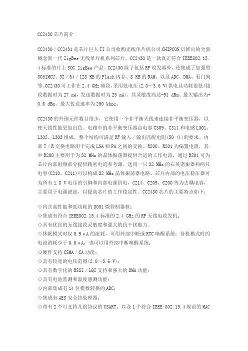
cc2430与cc2530区别
cc2430与cc2530区别CC2430与CC2530区别/doc/3eca50130b4e767f5acfce88.html 2530在内存、尺⼨、RF性能等⽅⾯⽐CC2430有了重⼤改进,如下表:类别CC2430 CC2530特征MCU 兼容8051 兼容8051Flash 128KB 256KBRAM 8K(<4K PM2/3) 8KB all PMs 时钟误差检查否是定时器1通道 3 5MAC定时器位数16-bit 20-bit 溢出16-bit 24-bit 溢出主频32MHz 32MHz封装7x7 , 48 pin 6x6, 40 pin⼯作环境- 40 ~ +85℃- 40 ~ +125℃⽆线性能灵敏度(dBm) - 92 - 97 最⼤发送功率(dBm) 0 + 4.592 101.5输出功率最⼤误差11% 2% 偏差-5MHz 30 49偏差+5MHz 41 49偏差-10MHz 53 57偏差+10MHz 55 57低功耗⼯作电压 2.0 ~ 3.6V 2.0 ~ 3.6V接收电流27 mA 24 mA 发送电流(0dBm) 27 mA 29 mA发送电流(+4.5dBm) N A 34mACPU有效电流(32MHz) 10.5mA 6.5mA PM1电流190 uA 200 uAPM2电流0.5 uA 1 uAPM3电流0.3uA 0.4uAPM1->有效 4 us 4 usPM2/3->有效0.1 ms 0.1 ms晶振启动时间0.5ms 0.3ms2.⼯具SmartRF05平台完全⽀持CC2530,同时SmartRF04平台完全⽀持CC2430。
SmartRF04EB 板发货时配有CC2430,也⽀持CC2530,但固件必须更新和不是所有的功能都有⽤。
SmartRF04EB 板没有软件栈和例程。
⽼版SmartRF05EB 板固件需要升级才能识别CC2530。
CC2530介绍
XTAL2 是一个可选的32.768-kHz 晶振,有两个负载电容(C321 和C331) 用于32.768-kHz晶振。32.768-kHz 晶振用于要求非常低的睡眠电流消耗和 精确唤醒时间的应用。32.768-kHz晶振看到的负载电容由下式给定:
串口
• 两种工作方式
– UART – SPI (可主可从)
内核
• • • • • • –优良的性能和具有代码预取功能的低功 耗 8051 微控制器内核 –32-、64-或 128-KB 的系统内可编程闪存 –8-KB RAM,具备在各种供电方式下的数 据保持能力 –支持硬件调试
低功耗
• • • • • • • –主动模式 RX(CPU 空闲):24 mA –主动模式 TX 在 1dBm(CPU 空闲):29 mA –供电模式 1(4 µs 唤醒):0.2 mA –供电模式 2(睡眠定时器运行):1 µA –供电模式 3(外部中断):0.4 µA –宽电源电压范围(2 V–3.6 V)
CC2530 外设
• • • • • • • 电源管理 RESET I/O DMA T1(16位) T2(MAC) T3/T4
• • • • • • • Sleep Timer ADC Random AES WDT UART Voltage Regulators
CC2530芯片内部结构
CC2530需要极少的外部连接元件,同时有很 多典型电路,其模块大致可以分为三类: 1、 CPU和内存相关模块 2、外设,时钟和电源管理相关模块 3、无线信号收发相关模块
存储器时的顺序,便于系统效率的提高。
•8 KB SRAM:超低功耗,使数字部分即使掉电也能保存其中内容,是芯片
低功耗原因所在。
•闪存块:用于保存电脑传输进入的程序代码以及常量数据,节约了搜寻时间。
CC2430芯片简介

有人形容高尔夫的18洞就好像人生,障碍重重,坎坷不断。
然而一旦踏上了球场,你就必须集中注意力,独立面对比赛中可能出现的各种困难,并且承担一切后果。
也许,常常还会遇到这样的情况:你刚刚还在为抓到一个小鸟球而欢呼雀跃,下一刻大风就把小白球吹跑了;或者你才在上一个洞吞了柏忌,下一个洞你就为抓了老鹰而兴奋不已。
CC2430芯片简介CC2430/CC2431是芯片巨人TI公司收购无线单片机公司CHIPCON后推出的全新概念新一代ZigBee无线单片机系列芯片。
CC2430是一款真正符合IEEE802.15. 4标准的片上SOC ZigBee产品。
CC2430除了包括RF收发器外,还集成了加强型8051MCU、32/64/128 KB的Flash内存、8 KB的RAM、以及ADC、DMA、看门狗等。
CC2430可工作在2.4 GHz频段,采用低电压(2.0~3.6 V)供电且功耗很低(接收数据时为27 mA,发送数据时为25 mA),其灵敏度高达-91 dBm、最大输出为+ 0.6 dBm、最大传送速率为250 kbps。
CC2430的外围元件数目很少,它使用一个非平衡天线来连接非平衡变压器,以使天线性能更加出色。
电路中的非平衡变压器由电容C309、C311和电感L301、L302、L303组成,整个结构可满足RF输入/输出匹配电阻(50 Ω)的要求。
内部T/R交换电路用于完成LNA和PA之间的交换。
R200、R201为偏置电阻,其中R200主要用于为32 MHz的晶体振荡器提供合适的工作电流,通过R201可为芯片内部射频部分提供精密电流参考源。
选用一只32 MHz的石英谐振器和两只电容(C210、C211)可以构成32 MHz晶体振荡器电路。
芯片内部的电压稳压器可为所有1.8 V电压的引脚和内部电源供电,C214、C209、C200等为去耦电容,主要用于电源滤波,以提高芯片的工作稳定性。
CC2430芯片的主要特点如下:◇内含高性能和低功耗的8051微控制器核;◇集成有符合IEEE802.15.4标准的2.4 GHz的RF无线电收发机;◇具有优良的无线接收灵敏度和强大的抗干扰能力。
- 1、下载文档前请自行甄别文档内容的完整性,平台不提供额外的编辑、内容补充、找答案等附加服务。
- 2、"仅部分预览"的文档,不可在线预览部分如存在完整性等问题,可反馈申请退款(可完整预览的文档不适用该条件!)。
- 3、如文档侵犯您的权益,请联系客服反馈,我们会尽快为您处理(人工客服工作时间:9:00-18:30)。
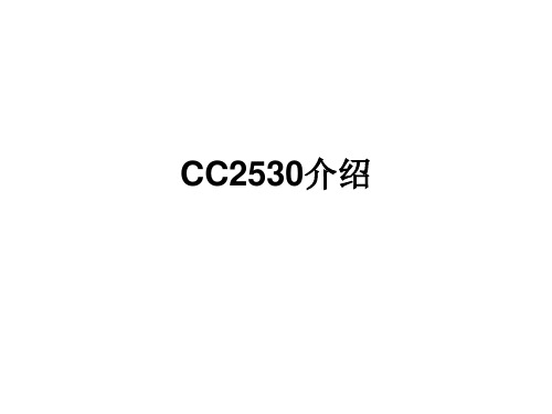
支持ZigBee协议的单片机有:msp430F1611、msp430F1612
段频
2.4G
2.4G
支持标准
ZigBee04/06/ SimpliciTI
ZigBee07/PRO/RF4CE/ SimpliciTI
软件平台
IAR
IAR
射频RF
CC2420
CC2520
接收灵敏度
-90dBm
-97dBm
典型值,802.15.4要求为-85dBm
输出功率
0(最小为-3)dBm
4.5(最小-8,最大10)dBm
典型值
自带传感器
温度
温度
功耗
RX:27mA
TX:25mA
RX:24mA
TX:29mA
低功耗
掉电:0.9uA
挂起:0.6uA
掉电:1uA
挂起:0.4uA
抗干扰
CSMA/CA
CSMA/CA
DMA
支持
支持
RSSI/LQI支持来自支持AES处理器有
有
I/O
21个
21个
定时/计数器
4(2个16位、2个8位)
4(2个16位、2个8位)
串口
2个
2个
802.15.4定时器
有
有
中断源
18个
18个
ADC
8-14位
7-12位
开发工具
C51RF-3-PK
C51RF-CC2530-PK
CC2530是TI 09年推出的,在CC2430的基础上根据CC2430实际应用的一些问题做了一些改进,缓存加大了,存储容量最大支持到256K,不用在为存储容量小而对代码进行限制,CC2530的通信距离可以达到400m,不用在用CC2430外加功放来扩展距离!
CC2530与2430的区别
无线个人网局域网2011-01-23 21:40:21阅读193评论0字号:大中小订阅
CC2530与2430的区别:
/xilinxue/225863/message.aspx
成都无线龙通讯公司推出CC2530PK系列产品,以下给出:ZigBee芯片CC2430 / CC2530对比一览表:
项目
CC2430
CC2530
备注
引脚
48
40
封装
QLP48
QFN40
电压
2.0V – 3.6V
2.0V – 3.6V
大小
7x7mm
6mm × 6mm
微控制器
增强型C8051
增强型C8051
Flash
32/64/128KB
32/64/128/256KB
RAM
8 KB SRAM, 4 KB Data
8KB