AH114-89PCB1900中文资料
SCPQ-90中文资料
JYPQ
LRPQ-J
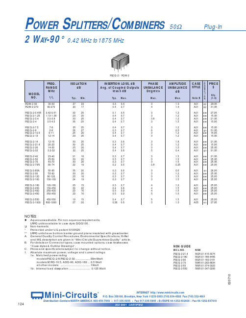
INSERTION LOSS, dB Avg. of Coupled Outputs less 3 dB
PHASE UNBALANCE
Degrees
Typ. Max.
0.2
0.7
0.2 0.7 0.2 0.7
0.45 1.4 0.5 1.0 0.2 0.5 0.2 0.6 0.5 1.1
21 18 30 20 30 20 22 19
35 20 30 20 25 18 24 19
23 15 30 22 23 16 23 16
19 15 27 20
PSCQ-2 / PQW-2
INSERTION LOSS, dB Avg. of Coupled Outputs
less 3 dB
Typ. Max.
1a. Matched power rating models PSCQ-2-8,PSCQ-2-32 ................... 50mWatt models SCPQ-10.5, ADQ-90, ADQ-180 ... 0.5 Watt all other models ...................................... 1Watt
6
7
3
6
NOT USED
—
—
—
—
—
gx 1 2 5 3,4,7,8 — — —
gy 1 2(0°) 6(90°) 3,4,7,8
5 —
hm
ja
9
1
2(0°)
8
6(-90°)
14
1,3,4,5,7,8 2,3,4,5,6,9
10,11,12,14 10,11,12,13
A22A中文资料
Connected Terminals
Up
Center Down
Slot
Slot
Throw & Schematics
Note: Terminal numbers are not actually on the switch.
OFF NONE
ON
OPEN OPEN
3-1
ON ON ON (ON) (ON) ON (ON)
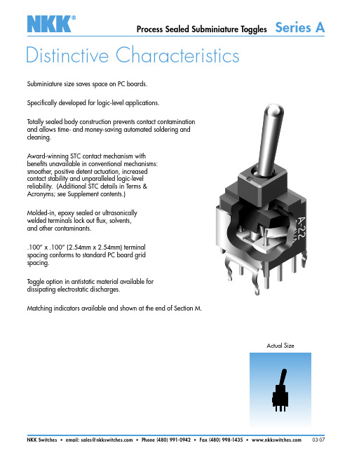
Actual Size
NKK Switches • email: sales@ • Phone (480) 991-0942 • Fax (480) 998-1435 • 03-07
元器件交易网
Series A Process Sealed Subminiature Toggles
Standards & Certifications
UL Recognition or CSA Certification: The A Series toggles have not been tested for UL recognition or CSA certification.
These switches are designed for use in a low-voltage, low-current, logic-level circuit. When used as intended in a logic-level circuit, the results do not produce hazardous energy.
.248” (6.3mm) Long Bat Toggle
SPDT ON-NONE-ON Circuit
Vertical PC Terminals
ZXFV4089N8TA中文资料(Zetex Semiconductors)中文数据手册「EasyDatasheet - 矽搜」

H 0.228 0.244
E 0.150 0.157
L 0.016 0.050
e
0.050 BSC
b 0.013 0.020
c 0.008 0.010
0
8
h 0.010 0.020
毫米为
MIN MAX
1.35 1.75
0.10 0.25
4.80 5.00
5.80 6.20
3.80 4.00
0.40 1.27
持续时间将在中央部施加
背部门廊间隔,从而使背部门廊或'黑'电平被钳位 到地.对于每一个行扫描,这给出一个亮度级与该原 始相机信号一致,尽管AC耦合.
耦合电容值会影响两个主要
电路特性.首先,现有 充电电流,与电容器值一起,
决定最大直流电压校正其
可以在每个样品被应用.为充电电流 300微安限制施加2微秒,注入电荷是
条件
P/C MIN
HOLD =高
P
HOLD =低
P
HOLD =高
P
HOLD =低
P
HOLD =高 HOLD =高 HOLD =高 HOLD =高 HOLD =高 HOLD =高 HOLD =高 HOLD =高 HOLD =高 HOLD =高 HOLD =高 HOLD =高
P P P P 500 P 1.5 P 48 P ±2.5 P 40 P 49 P 51 C P ±2.5
ZXFV4089N8TA ZXFV4089N8TC
集装箱
卷7" 卷13"
增量
500 2500
连接图
特点和优点 各种电视制式,PAL,NTSC,SECAM
采用高品质视频放大器缓冲输出
SPEC C89P104-01001AH

EIA 364-21, Apply DC 500r10% Volts between the inner contacts and the outer contact for one minute. EIA 364-20, Test Condition I Apply AC 200 V Vrms between the signal contacts and the ground contact for one minute.
Mate connector with a suitable gauge at rate of 25 mm/min. Measure force when gauge reaches surface of connector. EIA 364-05. The sample should be mounted in the tester and fully mated and unmated the number of cycles specified at the rate of 12 cycles/min EIA 364-09. Shown in Figure 4.
Plug can’t separate from cable. 700g Min
Shown in Figure 5. Speed of 25r3mm/minutes by the tensile strength machine and measure the retention force.
No electrical discontinuity greater than 1Ӵsecond. See Note (a). Signal:40 mӨ!Max. final Ground: 40 mӨ!Max. final
松川继电器892系列

ϬStandard Type
Terminal style
Contact UL Insulation form system approval
----------
Designation (provided with)
892H NO / NCΚ10A/5A 120VAC (50,000 ops.) NO / NCΚ7A/5A 240VAC NO / NCΚ10A/5A 277VAC NO / NCΚ1680VA/1200VA
Coil Rating (DC)
ϬStandard Type
114
Rated Rated current Coil resistance Max. continuous Pick up
F ----------
892-1AH-F-C 892-1CC-C
892-1AH-F-V 892-1CC-V
892-1AH-F-S 892-1CC-S
1C
F
892-1CC-F-C 892-1CC-F-V
892-1CC-F-S
(SPDT)
----------
892-1CH-C
892-1CH-V
892-1CH-S
Contact material Contact resistance (1) Operate time (1) Release time (1) Insulation resistance (1)
AgNi / Ag SnO alloy 100m7����������������������������������������������������������������������������������������������������������������������������������������������������������������������������������������������������������������������������������������������������������������������������������������������������������������������������������������������������������������������������������������������������������������������������������������������������������������������������������������������������������������������������������������������������������������������������������������������������������������������������������������������������������������������������������������������������������������������������������������������������������������������������������������������������������������������������������������������������������������������������������������������������������������������������������������������������������������������������������������������������������������������������������������������������������������������������������������������������������������������������������������������������������������������������������������������������������������������������������������������������������������������������������������������������������������������������������������������������������������������������������������������������������������������������������������������������������������������������������������������������������������������������������������������������������������������������������������������������������������������������������������������������������������������������������������������������������������������������������������������������������������������������������������������������������������������������������������������������������������������������������������������������������������������������������������������������������������������������������������������������������������������������������������������������������������������������������������������������������������������������������������������������������������������������������������������������������������������������������������������������������������������������������������������������������������������������������������������������������������������������������������������������������������������������������������������������������������������������������������������������������������������������������������������������������������������������������������������������������������������������������������������������������������������������������������
S29CD016J0JDGH114资料
This document contains information on one or more products under development at Spansion Inc. The information is intended to help you evaluate this product. Do not design in this product without contacting the factory. Spansion Inc. reserves the right to change or discontinue work on this proposed product without notice.Publication Number S29CD016J-CL016J_KGD_SP Revision A Amendment 2Issue Date September 20,2006General DescriptionThe Spansion S29CD016J and S29CL016J devices are Floating Gate products fabricated in 110 nm process technology. These burst mode Flash devices are capable of performing simultaneous read and write operations with zero latency on two separate banks. These products can operate up to 56 MHz and use a single V CC of 2.5 V to 2.75 V (S29CD-J) or 3.0 V to 3.6 V (S29CL-J) that make them ideal for today’s demanding automotive applications.Distinctive CharacteristicsSingle 2.6 V (S29CD-J) or 3.3 V (S29CL-J) for read/program/erase 110 nm Floating Gate TechnologySimultaneous Read/Write operation with zero latency X32 Data BusDual Boot Sector Configuration (top and bottom) Flexible Sector Architecture–CD016J & CL016J: Eight 2K Double word, Thirty-two 16K Double word, and Eight 2K Double Word sectorsVersatileI/O™ control (1.65 V to V CC ) Programmable Burst Interface–Linear for 2, 4, and 8 double word burst with or without wrap aroundSecured Silicon Sector that can be either factory or customer locked 20 year data retention (typical)Cycling Endurance: 100,000 write cycles per sector (typical) Command set compatible with JECEC (42.4) standard Supports Common Flash Interface (CFI)Persistent and Password methods of Advanced Sector Protection Unlock Bypass program command to reduce programming time Write operation status bits indicate program and erase operation completion Hardware (WP#) protection of two outermost sectors in the large bank Ready/Busy (RY/BY#) output indicates data available to system Suspend and Resume commands for Program and Erase OperationPerformance CharacteristicsS29CD016J/S29CL016J Known Good Die16 Megabit (512k x 32-Bit) CMOS 2.6 or 3.3 Volt-only Burst Mode, Dual Boot,Simultaneous Read/Write Flash MemorySupplement (Advance Information)Read Access TimesSpeed Option (MHz)5640Max Asynch. Access Time, ns (t ACC )6467Max Synch. Latency, ns (t IACC )6467Max Synch. Burst Access, ns (t BACC )1017Max CE# Access Time, ns (t CE )6971Max OE# Access time, ns (t OE )2222Current Consumption (Max values)Continuous Burst Read @ 56 MHz90 mA Program 50 mA Erase 50 mA Standby Mode150 µATypical Program and Erase TimesDouble Word Programming 18 µs Sector Erase1.0 sS u p p l e m e n t(A d v a n c e I n f o r m a t i o n)Table of ContentsGeneral Description . . . . . . . . . . . . . . . . . . . . . . . . . . . . . . . . . . . . . . . . . . . . . . . . . . . . . . . . . . . . . . . . . . . 1Distinctive Characteristics. . . . . . . . . . . . . . . . . . . . . . . . . . . . . . . . . . . . . . . . . . . . . . . . . . . . . . . . . . . . . . 1Performance Characteristics. . . . . . . . . . . . . . . . . . . . . . . . . . . . . . . . . . . . . . . . . . . . . . . . . . . . . . . . . . . . 1Table of Contents . . . . . . . . . . . . . . . . . . . . . . . . . . . . . . . . . . . . . . . . . . . . . . . . . . . . . . . . . . . . . . . . . . . . . 2S29CD/CL016J Features. . . . . . . . . . . . . . . . . . . . . . . . . . . . . . . . . . . . . . . . . . . . . . . . . . . . . . . . . . . . . . . . 31.Die Photograph. . . . . . . . . . . . . . . . . . . . . . . . . . . . . . . . . . . . . . . . . . . . . . . . . . . . . . . . . . . . . . . . . . . 42.Die Pad Locations . . . . . . . . . . . . . . . . . . . . . . . . . . . . . . . . . . . . . . . . . . . . . . . . . . . . . . . . . . . . . . . . 53.Pad Description . . . . . . . . . . . . . . . . . . . . . . . . . . . . . . . . . . . . . . . . . . . . . . . . . . . . . . . . . . . . . . . . . . 64.Ordering Information . . . . . . . . . . . . . . . . . . . . . . . . . . . . . . . . . . . . . . . . . . . . . . . . . . . . . . . . . . . . . . 84.1Valid Combinations . . . . . . . . . . . . . . . . . . . . . . . . . . . . . . . . . . . . . . . . . . . . . . . . . . . . . . . . . 85.Packaging Information. . . . . . . . . . . . . . . . . . . . . . . . . . . . . . . . . . . . . . . . . . . . . . . . . . . . . . . . . . . . . 95.1Surftape Packaging . . . . . . . . . . . . . . . . . . . . . . . . . . . . . . . . . . . . . . . . . . . . . . . . . . . . . . . . . 95.2Waffle Pack Packaging . . . . . . . . . . . . . . . . . . . . . . . . . . . . . . . . . . . . . . . . . . . . . . . . . . . . . 106.Product Test Flow. . . . . . . . . . . . . . . . . . . . . . . . . . . . . . . . . . . . . . . . . . . . . . . . . . . . . . . . . . . . . . . . 107.Absolute Maximum Ratings . . . . . . . . . . . . . . . . . . . . . . . . . . . . . . . . . . . . . . . . . . . . . . . . . . . . . . . 128.Operating Ranges . . . . . . . . . . . . . . . . . . . . . . . . . . . . . . . . . . . . . . . . . . . . . . . . . . . . . . . . . . . . . . . 129.Physical Specifications . . . . . . . . . . . . . . . . . . . . . . . . . . . . . . . . . . . . . . . . . . . . . . . . . . . . . . . . . . . 1310.Manufacturing Information . . . . . . . . . . . . . . . . . . . . . . . . . . . . . . . . . . . . . . . . . . . . . . . . . . . . . . . . 1311.Special Handling Instructions. . . . . . . . . . . . . . . . . . . . . . . . . . . . . . . . . . . . . . . . . . . . . . . . . . . . . . 1311.1Processing. . . . . . . . . . . . . . . . . . . . . . . . . . . . . . . . . . . . . . . . . . . . . . . . . . . . . . . . . . . . . . . 1311.2Storage . . . . . . . . . . . . . . . . . . . . . . . . . . . . . . . . . . . . . . . . . . . . . . . . . . . . . . . . . . . . . . . . . 1312.DC Characteristics for KGD Devices at 145°C. . . . . . . . . . . . . . . . . . . . . . . . . . . . . . . . . . . . . . . . . 1313.Terms and Conditions of Sale for Spansion Non-Volatile Memory Die. . . . . . . . . . . . . . . . . . . . . 1414.Revision Summary. . . . . . . . . . . . . . . . . . . . . . . . . . . . . . . . . . . . . . . . . . . . . . . . . . . . . . . . . . . . . . . 15List of FiguresFigure 6.1Spansion KGD Product Test Flow. . . . . . . . . . . . . . . . . . . . . . . . . . . . . . . . . . . . . . . . . . . . . 11Figure 7.1Maximum Negative Overshoot Waveform. . . . . . . . . . . . . . . . . . . . . . . . . . . . . . . . . . . . . . . 12Figure 7.2Maximum Positive Overshoot Waveform. . . . . . . . . . . . . . . . . . . . . . . . . . . . . . . . . . . . . . . . 12List of TablesTable 3.1Pads Relative To Die Center . . . . . . . . . . . . . . . . . . . . . . . . . . . . . . . . . . . . . . . . . . . . . . . . . .6Table 12.1DC Characteristics, CMOS Compatible . . . . . . . . . . . . . . . . . . . . . . . . . . . . . . . . . . . . . . . . .13 2S29CD016J/S29CL016J Known Good Die Revision A2September20,2006S u p p l e m e n t(A d v a n c e I n f o r m a t i o n)S29CD/CL016J FeaturesThe S29CD016J & S29CL016J Flash devices are burst mode, dual boot, simultaneous read/write Flashmemories with VersatileI/O™ manufactured on 110 nm process technology.The S29CD016J is a 16 megabit, 2.6 volt-only, single-power-supply, burst mode Flash memory device thatcan be configured for 524,288 double words. The S29CL016J is the 3.3 volt-only version of that device. Bothdevices can be programmed in standard EPROM programmers.To eliminate bus contention, each device has separate chip enable (CE#), write enable (WE#) and outputenable (OE#) controls. Additional control inputs are required for synchronous burst operations: Load BurstAddress Valid (ADV#), and Clock (CLK).Each device requires only a single 2.6 volt-only (2.50 V – 2.75 V) or 3.3 volt-only (3.00 V – 3.60 V) for bothread and write functions. A 12.0-volt V PP is not required for program or erase operations, although anacceleration pin is available if faster programming performance is required.The device is entirely command set compatible with the JEDEC single-power-supply Flash standard. Thesoftware command set is compatible with the command sets of the 5 V Am29F and 3 V Am29LV Flashfamilies. Commands are written to the command register using standard micro-processor write timing.Register contents serve as inputs to an internal state-machine that controls the erase and programmingcircuitry. Write cycles also internally latch addresses and data needed for the programming and eraseoperations. Reading data out of the device is similar to reading from other Flash or EPROM devices.The Unlock Bypass mode facilitates faster programming times by requiring only two write cycles to programdata instead of four.The Simultaneous Read/Write architecture provides simultaneous operation by dividing the memory spaceinto two banks. The device can begin programming or erasing in one bank, and then simultaneously readfrom the other bank, with zero latency. This releases the system from waiting for the completion of program orerase operations.The device provides a 256-byte Secured Silicon Sector with an one-time-programmable (OTP) mechanism.In addition, the device features several levels of sector protection, which can disable both the program anderase operations in certain sectors or sector groups: Persistent Sector Protection is a command sectorprotection method that replaces the old 12 V controlled protection method; Password Sector Protection is ahighly sophisticated protection method that requires a password before changes to certain sectors or sectorgroups are permitted; WP# Hardware Protection prevents program or erase in the two outermost 8 Kbytessectors of the larger bank.The device defaults to the Persistent Sector Protection mode. The customer must then choose if theStandard or Password Protection method is most desirable. The WP# Hardware Protection feature is alwaysavailable, independent of the other protection method chosen.The VersatileI/O™ (V CCQ) feature allows the output voltage generated on the device to be determined basedon the V IO level. This feature allows this device to operate in the 1.8 V I/O environment, driving and receivingsignals to and from other 1.8 V devices on the same bus.The host system can detect whether a program or erase operation is complete by observing the RY/BY# pin,by reading the DQ7 (Data# Polling), or DQ6 (toggle) status bits. After a program or erase cycle has beencompleted, the device is ready to read array data or accept another command.The sector erase architecture allows memory sectors to be erased and reprogrammed without affecting thedata contents of other sectors. The device is fully erased when shipped from the factory.Hardware data protection measures include a low V CC detector that automatically inhibits write operationsduring power transitions. The password and software sector protection feature disables both program anderase operations in any combination of sectors of memory. This can be achieved in-system at V CC level.The Program/Erase Suspend/Erase Resume feature enables the user to put erase on hold for any period oftime to read data from, or program data to, any sector that is not selected for erasure. True background erasecan thus be achieved.The hardware RESET# pin terminates any operation in progress and resets the internal state machine toreading array data.September20,2006Revision A2S29CD016J/S29CL016J Known Good Die3S u p p l e m e n t(A d v a n c e I n f o r m a t i o n)The device offers two power-saving features. When addresses have been stable for a specified amount oftime, the device enters the automatic sleep mode. The system can also place the device into the standbymode. Power consumption is greatly reduced in both these modes.Spansion Flash technology combines years of Flash memory manufacturing experience to produce thehighest levels of quality, reliability and cost effectiveness. The device electrically erases all bits within a sectorsimultaneously via Fowler-Nordheim tunnelling. The data is programmed using hot electron injection.1.Die Photograph4S29CD016J/S29CL016J Known Good Die Revision A2September20,2006S u p p l e m e n t(A d v a n c e I n f o r m a t i o n)2.Die Pad LocationsSeptember20,2006Revision A2S29CD016J/S29CL016J Known Good Die5S u p p l e m e n t(A d v a n c e I n f o r m a t i o n)3.Pad DescriptionTable 3.1 Pads Relative To Die Center (Sheet 1 of 2)Pad Description – Coordinates are Relative to Die CenterPad SignalMilsµmX Y X Y1VSS87.381 3.3472219.48585.0162VCC87.3818.0312219.485203.9943CE#87.38112.8922219.485327.4564OE#87.38117.5562219.485445.9215WE#87.38122.222219.485564.3866WP#87.38127.0392219.485686.7937IND/WAIT#88.34639.7412243.9861009.4328DQ(16)70.56246.961792.271192.7739DQ(17)65.79746.961671.241192.77310DQ(18)57.69146.961465.3561192.77311DQ(19)52.92646.961344.3261192.77312VCCQ46.446.961178.571192.77313V SS41.73846.961060.1531192.77314DQ(20)35.23546.96894.9571192.77315DQ(21)30.4746.96773.9271192.77316DQ(22)22.36446.96568.0431192.77317DQ(23)17.59946.96447.0131192.77318DQ(24)–0.09346.96–2.3561192.77319DQ(25)–4.85846.96–123.3861192.77320DQ(26)–12.96346.96–329.271192.77321DQ(27)–17.72846.96–450.31192.77322V CCQ–24.25446.96–616.0561192.77323V SS–28.91646.96–734.4741192.77324DQ(28)–35.4246.96–899.6691192.77325DQ(29)–40.18546.96–1020.6991192.77326DQ(30)–48.29146.96–1226.5831192.77327DQ(31)–53.05646.96–1347.6131192.77328A0–69.00649.02–1752.7411245.10829A1–73.7749.02–1873.7711245.10830A2–78.33349.02–1989.6711245.10831A3–88.47341.504–2247.2161054.19632A4–88.47336.941–2247.216938.29633A5–88.47332.176–2247.216817.26634A6–88.47327.613–2247.216701.36635A7–88.47322.848–2247.216580.33636A8–88.47318.285–2247.216464.43637V SS–88.47313.402–2247.216340.41438ACC–88.4738.245–2247.216209.41839V CC–88.473–11.899–2247.216–302.22440A9–88.473–17–2247.216–431.79441A10–88.473–21.905–2247.216–556.3876S29CD016J/S29CL016J Known Good Die Revision A2September20,2006September 20,2006Revision A2S29CD016J/S29CL016J Known Good Die 7S u p p l e m e n t (A d v a n c eI n f o r m a t i o n )42A11–88.473–26.468–2247.216–672.28743A12–88.473–31.233–2247.216–793.31744A13–88.473–35.796–2247.216–909.21745A14–88.473–40.561–2247.216–1030.24746A15–88.473–45.124–2247.216–1146.14747A16–78.333–49.192–1989.671–1249.46948A17–73.77–49.192–1873.771–1249.46949A18–69.006–49.192–1752.741–1249.46950DQ(0)–53.056–47.131–1347.613–1197.13351DQ(1)–48.291–47.131–1226.583–1197.13352DQ(2)–40.185–47.131–1020.699–1197.13353DQ(3)–35.42–47.131–899.669–1197.13354V CCQ –28.894–47.131–733.913–1197.13355V SS –24.232–47.131–615.496–1197.13356DQ(4)–17.728–47.131–450.3–1197.13357DQ(5)–12.963–47.131–329.27–1197.13358DQ(6)–4.858–47.131–123.386–1197.13359DQ(7)–0.093–47.131–2.356–1197.13360DQ(8)17.599–47.131447.013–1197.13361DQ(9)22.364–47.131568.043–1197.13362DQ(10)30.47–47.131773.927–1197.13363DQ(11)35.235–47.131894.957–1197.13364V CCQ 41.76–47.1311060.713–1197.13365V SS 46.422–47.1311179.131–1197.13366DQ(12)52.926–47.1311344.326–1197.13367DQ(13)57.691–47.1311465.356–1197.13368DQ(14)65.797–47.1311671.24–1197.13369DQ(15)70.562–47.1311792.27–1197.13370V CCQ 87.381–42.3832219.485–1076.5471RESET#87.381–36.4992219.485–927.06772CLK 87.381–31.3942219.485–797.40273RY/BY#88.346–19.0182243.986–483.06674ADV#87.381–11.3862219.485–289.199Table 3.1 Pads Relative To Die Center (Sheet 2 of 2)Pad Description – Coordinates are Relative to Die CenterPad Signal MilsµmX Y X Y8S29CD016J/S29CL016J Known Good Die Revision A2September 20,2006S u p p l e m e n t (A d v a n c eI n f o r m a t i o n )4.Ordering InformationThe order number (Valid Combination) is formed by the following:4.1Valid CombinationsValid Combinations list configurations planned to be supported in volume for this device. Consult your local sales office to confirm availability of specific valid combinations and to 0c\\heck on newly released combinations.S29CD016J S29CL016J0J D E I 004PACKING TYPE4=Surf Tape (2500 per reel)7=Waffle Pack (42 per waffle pack tray)ADDITIONAL ORDERING OPTIONS 15th Character – S29CD016J only:0= 7E, 08, 01/00 Autoselect ID 1= 7E, 36, 01/00 Autoselect ID 15th Character – S29CL016J only:0=7E, 46, 01/00 Autoselect ID16th Character – Top or Bottom Boot:1=Bottom Boot with Simultaneous Operation 3=Bottom Boot with No Simultaneous Operation TEMPERATURE RANGE H =Hot (–40°C to +145°C)DIE THICKNESS G =500 µm PACKAGE TYPE D =DieCLOCK FREQUENCY10th Character - Initial Burst Access Delay 0=5-1-1-1, 6-1-1-1, and above 1=4-1-1-111h Character - Frequency J =40 Mhz M =56 MhzDEVICE NUMBER/DESCRIPTION S29CD016J/S29CL016J16 Megabit (512K x 32-Bit) CMOS 2.6 or 3.3 Volt-only Burst Mode, Dual Boot, Simultaneous Read/Write Flash Memory Manufactured on 110 nm Floating Gate TechnologyS29CL016J/S29CL016J Valid CombinationsS29CD016J OJ, 1J, OMDGH01, 03, 11, 131M 03, 13S29CL016JOJ, 1J, OM, 1M01, 03S u p p l e m e n t(A d v a n c e I n f o r m a t i o n)5.Packaging Information5.1Surftape PackagingDirection of FeedSeptember20,2006Revision A2S29CD016J/S29CL016J Known Good Die9S u p p l e m e n t(A d v a n c e I n f o r m a t i o n)5.2Waffle Pack Packaging6.Product Test FlowFigure 6.1 provides an overview of Spansion’s Known Good Die test flow. For more detailed information, referto the S29CD016J/S29CL016J product qualification database. Spansion implements quality assuranceprocedures throughout the product test flow. These QA procedures also allow Spansion to produce KGDproducts without requiring or implementing burn-in. In addition, an off-line quality monitoring program (QMP)further guarantees Spansion quality standards are met on Known Good Die products.10S29CD016J/S29CL016J Known Good Die Revision A2September20,2006Figure 6.1 Spansion KGD Product Test FlowElectronic marking is programmed into every KGD for the purpose of traceability. The electronic marking contains wafer lot number, wafer number of origin, die location on the wafer, mask revision, test program revision, test dates, and speed grade. Figure 6.1 illustrates the steps where specific electronic marking information is programmed. For more information regarding electronic marking, reference the S29CD016J Electronic Marking Data Sheet Supplement.7.Absolute Maximum RatingsNotes1.Minimum DC voltage on input or I/O pins is –0.5 V . During voltage transitions, input at I/O pins may overshoot V SS to –2.0 V for periods ofup to 20 ns. See Figure 7.1. Maximum DC voltage on output and I/O pins is 3.0 V . During voltage transitions output pins may overshoot to V CC + 2.0 V for periods up to 20 ns. See Figure 9.2.Minimum DC input voltage on pins ACC, A9, OE#, and RESET# is –0.5 V . During voltage transitions, A9, OE#, and RESET# mayovershoot V SS to –2.0 V for periods of up to 20 ns. See Figure 7.2. Maximum DC input voltage on pin A9 and OE# is +13.0 V which may overshoot to 13.7 V for periods up to 20 ns.3.No more than one output may be shorted to ground at a time. Duration of the short circuit should not be greater than one second.4.Stresses above those listed under Absolute Maximum Ratings may cause permanent damage to the device. This is a stress rating only;functional operation of the device at these or any other conditions above those indicated in the operational sections of this data sheet is not implied. Exposure of the device to absolute maximum rating conditions for extended periods may affect device reliability.Figure 7.1 Maximum Negative Overshoot WaveformFigure 7.2 Maximum Positive Overshoot Waveform8.Operating RangesNoteOperating ranges define those limits between which the functionality of the device is guaranteed.ParameterRating Storage Temperature–65°C to +150°C Ambient T emperature with Power Applied –65°C to +145°C V CC , V IO (Note 1)S29CD016J –0.5 V to + 3.0 V V CC , V IO (Note 1)S29CL016J–0.5 V to + 3.6 V ACC, A9, OE#, and RESET# (Note 2)–0.5 V to +13.0 V Address, Data, Control Signals (with the exception of CLK) (Note 1)–0.5 V to +3.6 V All other pins (Note 1)–0.5 V to +3.6 VOutput Short Circuit Current (Note 3)200mAParameterRating Ambient T emperature (T A), Hot Range –40°C to +145°CV CC Supply Voltage for regulated voltage range CD016J 2.5 V to 2.75 V CL016J3.0 V to 3.6 V V IO Supply Voltage1.65 V to V CC9.Physical Specifications10.Manufacturing Information11.Special Handling Instructions11.1ProcessingDo not expose KGD products to ultraviolet light or process them at temperatures greater than 250°C. Failure to adhere to these handling instructions will result in irreparable damage to the devices. For best yield, Spansion recommends assembly in a Class 10K clean room with 30% to 60% relative humidity.11.2StorageStore at a maximum temperature of 30°C in a nitrogen-purged cabinet or vacuum-sealed bag. Observe all standard ESD handling procedures.12.DC Characteristics for KGD Devices at 145°CSpecification Value Die Dimensions 4.77 x 2.83 mmDie Thickness 500 µm Bond Pad Size86 x 86 µm Pad Area Free of Passivation 5,776 µm 2Pads Per Die74Bond Pad Metalization Al/Cu PassivationSi02/SiNItem Description Location/Data Manufacturing Location Fab 25, TX T est LocationPNG Shipment Preparation Location Penang, MalaysiaManufacturing ID (Bottom Boot)98P05AB Fabrication Process CS69S Die Revision1Table 12.1 DC Characteristics, CMOS CompatibleParameter DescriptionTest ConditionMinTypMax Unit I CC1V CC Active Asynchronous Read CurrentCE# = V IL , OE#=V IL1 MHz10mA I CC3V CC Active Program Current CE# = V IL , OE#=V IL , ACC = V IH 4050mA I CC5 (Note 1)V CC Standby Current (CMOS)V CC = V CCMAX , CE# = V CC ± 0.3 V 250µA I CC7 (Note 1)V CC Reset CurrentReset = V IL250µA I CC8 (Note 1)Automatic Sleep Mode CurrentV IH = V CC ± 0.3 V, V IL = VSS ± 0.3 V250µA13.Terms and Conditions of Sale for Spansion Non-Volatile Memory DieAll transactions relating to unpackaged die under this agreement shall be subject to Spansion’s standardterms and conditions of sale, or any revisions thereof, which revisions Spansion reserves the right to make atany time and from time to time. In the event of conflict between the provisions of Spansion’s standard termsand conditions of sale and this agreement, the terms of this agreement shall be controlling.Spansion warrants its manufactured unpackaged die whether shipped to customer in individual dice or waferform (“Known Good Die,” “KGD”, “Die,” “Known Good Wafer”, “KGW”, or Wafer(s)) will meet Spansion'spublished specifications and against defective materials or workmanship for a period of one (1) year fromdate of shipment.This limited warranty does not extend beyond the first purchaser of said Die or Wafer(s).Buyer assumes full responsibility to ensure compliance with the appropriate handling, assembly andprocessing of KGD or KGW (including but not limited to proper Die preparation, Die attach, backgrinding,singulation, wire bonding and related assembly and test activities), and compliance with all guidelines setforth in Spansion's specifications for KGD or KGW, and Spansion assumes no responsibility forenvironmental effects on KGD or KGW or for any activity of Buyer or a third party that damages the Die orWafer(s) due to improper use, abuse, negligence, improper installation, improper backgrinding, impropersingulation, accident, loss, damage in transit, or unauthorized repair or alteration by a person or entity otherthan Spansion (“Limited Warranty Exclusions”)The liability of Spansion under this limited warranty is limited, at Spansion's option, solely to repair the Die orWafer(s), to send replacement Die or Wafer(s), or to make an appropriate credit adjustment or refund in anamount not to exceed the original purchase price actually paid for the Die or Wafer(s) returned to Spansion,provided that: (a) Spansion is promptly notified by Buyer in writing during the applicable warranty period ofany defect or nonconformity in the Die or Wafer(s); (b) Buyer obtains authorization from Spansion to returnthe defective Die or Wafer(s); (c) the defective Die or Wafer(s) is returned to Spansion by Buyer inaccordance with Spansion's shipping instructions set forth below; and (d) Buyer shows to Spansion'ssatisfaction that such alleged defect or nonconformity actually exists and was not caused by any of theabove-referenced Warranty Exclusions. Buyer shall ship such defective Die or Wafer(s) to Spansion viaSpansion's carrier, collect. Risk of loss will transfer to Spansion when the defective Die or Wafer(s) isprovided to Spansion's carrier. If Buyer fails to adhere to these warranty returns guidelines, Buyer shallassume all risk of loss and shall pay for all freight to Spansion's specified location. The aforementionedprovisions do not extend the original limited warranty period of any Die or Wafer(s) that has either beenreplaced by Spansion.THIS LIMITED WARRANTY IS EXPRESSED IN LIEU OF ALL OTHER WARRANTIES, EXPRESSED ORIMPLIED, INCLUDING THE IMPLIED WARRANTY OF FITNESS FOR A PARTICULAR PURPOSE, THEIMPLIED WARRANTY OF MERCHANTABILITY OR NONINFRINGEMENT AND OF ALL OTHEROBLIGATIONS OR LIABILITIES ON Spansion's PART, AND IT NEITHER ASSUMES NOR AUTHORIZESANY OTHER PERSON TO ASSUME FOR Spansion ANY OTHER LIABILITIES. THE FOREGOINGCONSTITUTES THE BUYER'S SOLE AND EXCLUSIVE REMEDY FOR THE FURNISHING OFDEFECTIVE OR NON CONFORMING KNOWN GOOD DIE OR KNOWN GOOD WAFER(S) AND SpansionSHALL NOT IN ANY EVENT BE LIABLE FOR INCREASED MANUFACTURING COSTS, DOWNTIMECOSTS, DAMAGES RELATING TO BUYER'S PROCUREMENT OF SUBSTITUTE DIE OR WAFER(S) (i.e.,“COST OF COVER”), LOSS OF PROFITS, REVENUES OR GOODWILL, LOSS OF USE OF ORDAMAGETO ANY ASSOCIATED EQUIPMENT, OR ANY OTHER INDIRECT, INCIDENTAL, SPECIAL ORCONSEQUENTIAL DAMAGES BY REASON OF THE FACT THAT SUCH KNOWN GOOD DIE OR KNOWNGOOD WAFER(S) SHALL HAVE BEEN DETERMINED TO BE DEFECTIVE OR NON CONFORMING.Buyer agrees that it will make no warranty representations to its customers which exceed those given bySpansion to Buyer unless and until Buyer shall agree to indemnify Spansion in writing for any claims whichexceed Spansion's limited warranty. Known Good Die or Known Good Wafer(s) are not designed orauthorized for use as components in life support appliances, devices or systems where malfunction of the Dieor Wafer(s) can reasonably be expected to result in a personal injury. Buyer's use of Known Good Die orKnown Good Wafer(s) for use in life support applications is at Buyer's own risk and Buyer agrees to fullyindemnify Spansion for any damages resulting in such use or sale.Known Good Die or Known Good Wafer are not designed or authorized for use as components in life supportappliances, devices or systems where malfunction of the die or wafer can reasonably be expected to result ina personal injury. Buyer's use of Known Good Die or Known Good Wafer for use in life support applications isat Buyer's own risk and Buyer agrees to fully indemnify Spansion for any damages resulting in such use orsale.。
解码板资料

VCD-380G/390G/部分360A/380A等机型,整机方案为SUNPLUS解码+PHILIPS伺服+PHILIPS光头。
其主要特点有:宽电源170V-242V;兼容MP3碟片;具备S端子输出、RF转换端口;图像放大、卡拉O K自动接唱;还具有游戏功能(只兼容公司附送的专用游戏碟片)等。
本机电路主要IC功能简介:二、RF、SSP及DSP处理电路伺服电路的组成:由RF放大器TDA1300T(U5),伺服及DSP处理电路SAA 7327(U6),聚焦、循迹驱动AM2088A(U8),主轴、进给驱动AM2088AH(U7)等组成。
1、RF数字信号处理从光盘反射回来的激光信号经光敏器件转换成电信号ID1~ID5,输入RF放大集成电路 TDA1300 Pin20~24;经内部放大和频率补偿后从Pin9输出RF信号,通过电容C85、C61、电阻R7 5到DSP处理SAA7327H Pin2,经内部EFM解调、纠错和数据处理后,变换为CD-DATA、CD-LRCK、CD -BCK信号,分别从Pin26~29输出至MPEG-1电路进行解压缩处理。
2、伺服处理1)聚焦伺服:从激光头拾取的激光电信号经TDA1300 RF放大后从Pin4、Pin3、Pin1输出聚焦误差信号送伺服处理SAA7327H Pin8~11,由内部处理成数字聚焦误差信号,经PWM调制为聚焦误差信号F O,从Pin55输出到伺服驱动放大AM2088A Pin2,经其内部驱动电路功率放大后,由Pin13、Pin16输出聚焦伺服电压信号FOC-、FOC+,驱动聚焦线圈上、下微移来促使物镜上下微移,从而校正激光焦点准确地落在光盘信息层。
2)循迹伺服:当光束偏离信息轨迹时,光敏二极管检测出误差信号E、F输出至RF放大TDA1300 Pin20、Pin23,经芯片内部处理后从Pin5、Pin2输出送到伺服处理SAA7327H Pin13、Pin12,由内部处理成数字循迹误差信号,再经PWM调制为循迹信号RA,由其Pin54输出至伺服驱动放大AM2088APin6,经其内部驱动电路功率放大后,由Pin9、Pin12输出循迹伺服电压信号RAD+、RAD-,驱动循迹线圈左、右微移来促使物镜左右微移,从而校正激光束准确跟踪光盘信息轨迹中心。
导向机电技术有限公司KS114技术说明书

KS114技术说明书版本:Ver.1.05创新技术源自导向技术深圳市导向机电技术有限公司Dauxi Technologies Co.,Ltd.All rights reserved.Modify Date Content Edit Revsion Note Nov.22,2019Parameter revision L.Q.B. 1.00Initial release. Jun.3,2020Beam angle added.X.T.C. 1.01Page5.Nov.23,2020Increase the content of reference assemblydimensions.X.Y.C. 1.02Please refer to Page23.Dec.21,2020Increase the ID and the protocol withverification.X.Y.C. 1.03Please refer to Page17.Sep.12,2021The assembly size of the KS114increases thecontrol tolerance.Y.M.G. 1.04Please refer to Page23.Sep.6,2022Add command“0x14”“0x1e”X.T.C. 1.05Page5,8,18:目录KS114功能摘要: (3)KS114电性能参数 (3)编码规则注解 (4)探测范围图 (5)I2C模式 (6)KS114连线及说明: (6)修改I2C地址时序: (7)KS114工作流程: (7)探测指令 (8)距离探测 (11)电源降噪指令(0x70,0x71,0x72,0x73,0x74,0x75)、波特率指令(0x77/0x78/0x79)波束角配置指令(0x7a-0x7e/0x80/0x81/0x82) (11)时序图 (12)休眠等待时间设置 (13)TTL串口及485串口模式 (14)TTL及485串口模式接线 (14)修改串口地址时序 (15)KS114工作流程 (15)探测结束智能识别 (17)探测指令 (17)电源降噪指令(0x70,0x71,0x72,0x73,0x74,0x75)、波特率指令(0x77/0x78/0x79)波束角配置指令(0x7a-0x7e/0x80/0x81/0x82) (20)时序图 (21)完整发货清单 (21)KS114装配尺寸图: (22)安装孔建议: (23)装配注意事项: (23)使用建议: (24)附件-例程: (25)KS114功能摘要:●IP65防水(IP67防水型号KS204/KS214),收发分体式设计,针对KS106/KS106A/KS136/KS136A的双探头版本设计;●主板与探头封装在一起,输出信号为数字量距离信号,与KS103类似;●可软件配置的波束角水平100°竖直50°或水平90°竖直40°;●探测范围:1cm-3m(常用1cm-1.5米。
- 1、下载文档前请自行甄别文档内容的完整性,平台不提供额外的编辑、内容补充、找答案等附加服务。
- 2、"仅部分预览"的文档,不可在线预览部分如存在完整性等问题,可反馈申请退款(可完整预览的文档不适用该条件!)。
- 3、如文档侵犯您的权益,请联系客服反馈,我们会尽快为您处理(人工客服工作时间:9:00-18:30)。
Typical Performance (1)
Units
MHz MHz dB dB dB dBm dBm dBm dB MHz dB dBm dBm mA V
Min
60 13.5
Typ
1900 14.5 10 14 +23 +41 +17 5.0 2140 14 +23 +40 150 +5
Absolute Maximum Rating
Parameter
Operating Case Temperature Storage Temperature RF Input Power (continuous) Device Voltage Device Current Junction Temperature
S-Parameters (Vcc = +5 V, Icc = 150 mA, T = 25 C, unmatched 50 ohm system)
1.0
30
6 0.
2. 0
0 3.
4. 0
0. 2
Gain (dB)
10.0
5 0 0 0.5 1 1.5 Frequency (GHz) 2 2.5 3
元器件交易网
AH114
¼ Watt, High Linearity InGaP HBT Amplifier
The Communications Edge TM Product Information
Product Features
60 – 2500 MHz +24 dBm P1dB +41 dBm Output IP3 19 dB Gain @ 900 MHz 14.5 dB Gain @ 1900 MHz +5V Single Positive Supply Lead-free / Green / RoHScompliant SOT-89 Package
.4 -0
.4 -0
.0 -2
-0 .6
-0.8
-0 .6
Swp Min 0.05GHz
-0.8
.0 -2
Swp Min 0.05GHz
-1.0
Notes: The gain for the unmatched device in 50 ohm system is shown as the trace in black color. For a tuned circuit for a particular frequency, it is expected that actual gain will be higher, up to the maximum stable gain. The maximum stable gain is shown in the dashed red line. The impedance plots are shown from 50 – 3000 MHz, with markers placed at 0.5 – 3.0 GHz in 0.5 GHz increments. S-Parameters (Vcc = +5 V, Icc = 150 mA, T = 25 C, unmatched 50 ohm system, calibrated to device leads)
-7.74 -7.80 -6.40 -6.33 -6.09 -5.86 -5.68 -5.58 -5.37 -5.20 -5.20 -5.05 -5.01 -4.89 -4.88 -4.73 -4.66
-1.0
-128.38 -143.29 -169.43 -179.95 173.78 168.37 163.12 157.73 152.46 147.09 141.71 136.43 131.29 126.16 121.19 116.28 111.40
Function Input / Base Output / Collector Ground
Pin No. 1 3 2, 4
Specifications (1)
Parameters
Operational Bandwidth Test Frequency Gain Input Return Loss Output Return Loss Output P1dB Output IP3 (2) IS-95A Channel Power
-30.46 -29.57 -27.97 -27.96 -27.96 -27.96 -26.02 -26.02 -26.02 -26.02 -25.08 -24.44 -24.44 -24.44 -23.27 -23.10 -23.10
17.14 14.05 9.40 10.86 10.86 10.62 9.88 8.87 7.57 5.95 4.22 2.37 0.24 -2.39 -5.53 -9.13 -12.86
Specifications and information are subject to change without notice
Operation of this device above any of these parameters may cause permanent damage.
WJ Communications, Inc Phone 1-800-WJ1-4401 FAX: 408-577-6621 e-mail: sales@ Web site:
Max
2500
Parameters
Frequency S21 - Gain S11 - Input R.L. S22 - Output R.L. Output P1dB Output IP3 Noise Figure Supply Bias
Units
MHz dB dB dB dBm dBm dB
Typical
130
170
1. Test conditions unless otherwise noted: 25 ºC, Vsupply = +5 V, in tuned application circuit. 2. 3OIP measured with two tones at an output power of +11 dBm/tone separated by 1 MHz. The suppression on the largest IM3 product is used to calculate the 3OIP using a 2:1 rule.
Freq (MHz) S11 (dB) S11 (ang) S21 (dB) S21 (ang) S12 (dB) S12 (ang) S22 (dB) S22 (ang)
50 100 200 400 600 800 1000 1200 1400 1600 1800 2000 2200 2400 2600 2800 3000
23.08 21.93 19.02 17.74 16.69 15.62 14.57 13.55 12.54 11.65 10.70 9.91 9.13 8.46 7.85 7.22 6.62
149.67 148.90 146.43 136.11 123.77 111.53 101.13 91.40 82.69 74.35 66.99 59.96 53.84 47.68 41.30 34.74 27.78
-3.61 -3.31 -2.62 -2.62 -2.54 -2.39 -2.27 -2.21 -2.16 -2.05 -1.99 -1.84 -1.68 -1.46 -1.33 -1.20 -1.17
-169.14 -173.35 179.12 173.23 168.30 163.31 158.06 152.89 147.55 142.54 137.85 133.47 129.41 125.20 120.48 115.03 109.05
Hale Waihona Puke Rating-40 to +85 C -65 to +150 C +15 dBm +6 V 220 mA +250 C
Ordering Information
Part No.
AH114-89G
Description
¼ Watt, High Linearity InGaP HBT Amplifier
900 1900 2140 19 14.5 14 -14 -10 -25 -10 -14 -20 +24 +23 +23 +40 +41 +40 5.0 5.0 6.0 +5 V @ 150 mA
+39.5
Noise Figure Test Frequency Gain Output P1dB Output IP3 (2) Operating Current Range Device Voltage
Page 1 of 6 November 2006
元器件交易网
AH114
¼ Watt, High Linearity InGaP HBT Amplifier
The Communications Edge TM Product Information
Typical Device Data
Device S-parameters are available for download off of the website at:
Application Circuit PC Board Layout
(lead-free/green/RoHS-compliant SOT-89 Pkg)
AH114-89PCB900 900 MHz Evaluation Board AH114-89PCB1900 1900 MHz Evaluation Board AH114-89PCB2140 2140 MHz Evaluation Board